Abstract
This paper will review the history of the scale-up of the pulsed laser deposition (PLD) process from small areas ∼1 cm2 up to 10 m2 starting in about 1987. It also documents the history of commercialization of PLD as various companies become involved in selling fully integrated laser deposition tools starting in 1989. The paper will highlight the current state of the art of commercial PLD equipment for R&D that is available on the market today from mainstream vendors as well as production-oriented applications directed at piezo-electric materials for microelectromechanical systems and high-temperature superconductors for coated-conductor applications. The paper clearly demonstrates that considerable improvements have been made to scaling this unique physical vapour deposition process to useful substrate sizes, and that commercial deposition equipment is readily available from a variety of vendors to address a wide variety of technologically important thin-film applications.
Export citation and abstract BibTeX RIS

Content from this work may be used under the terms of the Creative Commons Attribution 3.0 licence. Any further distribution of this work must maintain attribution to the author(s) and the title of the work, journal citation and DOI.
1. Introduction
Since 1987 when Dijkkamp et al [1] published their ground breaking paper on pulsed laser deposition (PLD) of Y1 Ba2 Cu3 O7−x (YBCO) there has been enormous interest and growth in the use of this unique physical vapour deposition (PVD) process. This paper will cover the initial history of the scale-up of PLD to large areas and the current state of commercial PLD equipment that is available today from multiple 'mainstream' vendors. The focus will be on an overview of available PLD equipment, basic capabilities, and some thin-film results ranging from 1 cm2 samples to metal tapes 1 km long by 1 cm wide with an effective area of 10 m2. The market for large-area production-oriented PLD tools has been constantly increasing over the past two decades. While it is hard to calculate current annual worldwide sales for production-oriented equipment it is estimated to be on the order of $10–$20 M USD/year and growing at ∼20% per year. The price of production-oriented lasers is included in this estimate.
In the early days of PLD (and here I am ignoring the early work of Smith and Turner who were the first to use PLD back in 1965 with a ruby laser [2]) people thought that the process was a novelty and would never be used for samples above ∼1 cm2. Even today it is surprising to find that people actually working on PLD still think PLD is just a small-area phenomenon and are not aware of all the considerable work that has been ongoing since 1987 to scale the process up to large-area or for production applications. Currently there are several companies that make production-oriented equipment for large-area processes, as we shall see. The choice of PLD for these production applications is due to the very high quality of the deposited films as well as its unique ability to easily grow complex multi-component materials with the proper stoichiometry [3, 4]. It should be pointed out that the ability to obtain higher quality and lower cost high-power excimer lasers for PLD R&D and production applications has been driven by the needs of laser processing in the areas of annealing amorphous silicon, ink-jet printer cartridges (hole drilling) and photo-lithography. PLD has been able to capitalize on the technological advancements realized in significantly improved excimer laser capability in terms of power, stability and reliability. Also, the continual development of new shorter pulse length lasers with high power has been interesting for PLD applications [4–8].
First, I will review the early history of the scale-up of PLD to large areas as well as the involvement of various companies who make PLD equipment. I will then present an overview of the current state of the art of commercial R&D PLD equipment along with matrix assisted pulsed laser evaporation (MAPLE), resonant IR MAPLE and resonant IR pulsed laser evaporation (RIRPLE) systems, and then move to more production-oriented excimer-based large-area PLD equipment.
2. Early history of large-area PLD and its commercialization
We go back to the 'early days' of the discovery of high-temperature superconductor (HTS) materials and the 'rediscovery' of PLD by Venkatesan's Bellcore group using shorter wavelength excimer lasers (1987). Once this paper was published there was a tremendous wave of excitement in the materials science community and substantial in-house building of PLD tools. All these tools were clearly focused on small areas—typically about 1 cm2 in size. In order to scale the process up there were multiple obstacles that would need to be developed to make the PLD process more than just a unique small-area R&D tool. These obstacles included laser beam scanning techniques used in conjunction with large-diameter targets, substrate rotation with blackbody substrate heaters, ways to keep the laser beam path clean for extended periods of time, in situ diagnostics, to name a few. Few people were considering the scale-up of PLD at this time as everyone was focused on making small samples of high-quality YBCO and other complex oxide thin films. For this process to become a large-area technique and capable of being used in production applications it would require significant effort and vision to move the process forward.
While working at the Research Division of Raytheon Corporation I started working with excimer lasers for a laser-induced forward transfer (LIFT) process to accurately set the frequency of hermetically sealed surface acoustic wave (SAW) devices [9] and had recently purchased an excimer laser and microscope for conducting this work. This process went into production at Raytheon in the early 1990s (the first production application of LIFT) and is still extensively used in production today to fabricate almost all the SAW devices used in a wide array of military radar and communication applications. I had put in a request for funding at the Research Division for my next year's capital budget for a generic 'laser-processing tool' to make better use of the excimer laser that was purchased just for the SAW LIFT process. I was thinking of photolytic direct write deposition processing of materials at the time. When the work of Venkatesan and Dijkkamp was published I was very lucky in that I had the available funds already approved to build a laser process tool. Thus, I decided to build a 'large-area' PLD tool. I had been currently working on PLD of YBCO in a home-built PLD system in a 4.5 inch CF cube on small 1 cm square samples soon after the Bellcore publication and making very little progress. I then spent about four months and drew using paper and pencil a 'large-area' PLD tool that was originally designed to deposit films onto 75 mm diameter wafers. At this point I had not heard the news that PLD was just a small-area process.
Figure 1 shows a photo of the world's first large-area PLD tool built by the author at the Research Division of Raytheon. It utilized laser beam scanning with a single large-diameter target, and eventually an Intelligent Window and a blackbody substrate heater that provided heating of Si to 950 °C and transparent substrates such as sapphire and LaAlO3 to high temperatures of 850 °C without the use of silver paste (which was popular at the time). The system also included an atomic oxygen source from ASTeX, now owned by MKS Instruments.
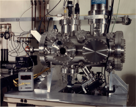
Figure 1. The world's first large-area PLD tool designed and developed at the Research Division of Raytheon in 1988. This tool was used to grow films on samples ranging in size from 75 mm up to 200 mm in diameter.
Download figure:
Standard image High-resolution imageWhile working on PLD of YBCO on LaAlO3 substrates it became apparent that heating transparent substrates was a difficult task. Thus, a scheme to put the wafer into a furnace or blackbody was developed. It is interesting that this is not typically possible to do for most other PVD techniques due to flux geometries. Figure 2 shows a photo of the original blackbody substrate heater assembly incorporated in this chamber. This heater included multiple heating elements located above, circumferentially around the wafer edges, as well as below the substrate surface (just above the target) along with several sets of reflecting shields. The elements were made from Pt/Rh wire inserted into dual-bore alumina tubes. Figure 2 shows the top (a) and bottom (b) portion of the blackbody substrate heater assembly, respectively. In figure 2(a) the substrate rotation shaft is seen protruding through of the top heater elements. This shaft was used to fix the substrate holder in place and was connected to motorized rotary feedthrough on the atmosphere side of the chamber. As can be seen in the photograph there is a set of ceramic heater elements that heat the sample from the top, as well as a set of elements that are seen coming straight down around the sides of the heater.
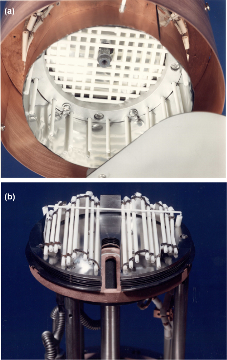
Figure 2. (a) Photograph of the upper blackbody substrate heater assembly showing heating elements that radiate onto the top of the substrate holder (not seen) as well as elements that radiate onto the substrate from the sides. (b) Lower blackbody substrate heater assembly showing the YBCO target seen through the slot, water-cooled copper plate, several Inconel shields, and then a bank of ceramic tubes with Pt/Rh heating wire.
Download figure:
Standard image High-resolution imageIn figure 2(b) the lower heater assembly is seen. These lower heating elements were used to radiate onto the front side of the sample surface. There is a slot in the shields and a water-cooled copper plate that allowed the laser beam to be rastered back and forth across the YBCO target which is visible within the slot. With this arrangement, the substrate was in essence put into a furnace or blackbody and heated from all sides. Thus, materials such as LaAlO3, sapphire, etc would have to rise to high temperatures as defined by the radiation environment and one could easily achieve temperatures of 850 °C. Modern day blackbody heaters utilize lamps and can heat silicon to over 1000 °C if required.
This PLD tool was state of the art for large-area PLD films for almost a decade. It was used to deposit double-sided high-quality YBCO films on 75 mm diameter LaAlO3 substrates in 1991, and eventually to deposit films on 150 and 200 mm diameter Si wafers [3, 4, 10–12].
Figure 3 shows a photograph of a 570 nm thick Y2O3 film deposited onto a 200 mm diameter Si wafer using the Raytheon large-area PLD chamber in late 1994. The growth rate of this film was 0.57 µm h−1 with ∼20 W of power on target at 248 nm and a 125 mm target-to-substrate distance. The film thickness non-uniformity of this wafer as measured by ellipsometry was better than ±3.5% [4]. Similarly, the composition of a 1 µm thick PLD Y1 Ba2 Cu3 O7−x film deposited onto a 150 mm diameter Si wafer was also shown to be very uniform [4]. These results obtained 19 years ago clearly indicated that PLD was a scalable process and could be used for large-area real world applications.
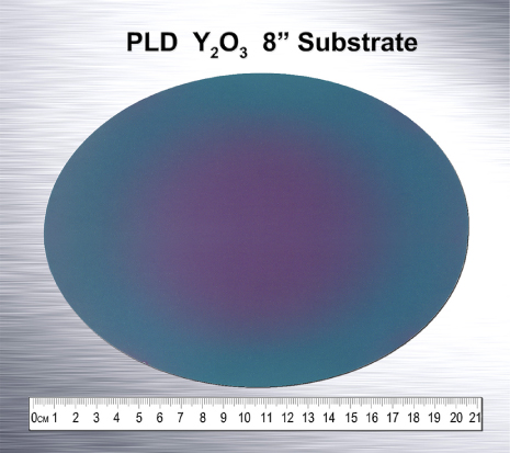
Figure 3. Photo of a 570 nm thick Y2O3 film deposited onto a 200 mm diameter Si wafer via PLD in 1994. Film thickness non-uniformity was better than that of ±3.5% as measured by ellipsometry [4].
Download figure:
Standard image High-resolution imageSeveral other groups also started to scale up the PLD process including that of the Lorenz group in Leipzig who also grew double-sided YBCO films on 75 mm diameter r-plane sapphire substrates in 1996 [14]. These films were then used by Bosch for microwave filter and satellite communication applications. In that time frame, Superconductor Technology, Inc. was using PLD to deposit the precursor elements of thallium based superconductors onto multiple 2 inch wafers at a time. Also about this time, Westinghouse had a program and was using off-set PLD [3] and was growing films on 100 mm diameter wafers. Many other groups not mentioned here also started their own programs scaling up the PLD process to larger diameter wafers.
While conducting deposition utilizing the large-area PLD chamber at Raytheon for various technological materials, in particular thin-film phosphors [13], it became apparent that coating of the laser optic that allowed the laser beam to enter the chamber would become a serious problem for large-area and/or thick films, as well as for load-locked PLD systems. Thus, the Intelligent Window [4] was developed in 1992 to resolve this issue. The Intelligent Window utilizes a large fused silica disc inside the vacuum chamber located just behind a high-quality AR-coated laser optic that makes the atmosphere/vacuum interface. An internal aperture on the other side of the disc within the unit defines the area that the laser beam can impinge on the target as well as a small well-defined area of the internal disc that will be coated by the backscattered ablated material. When the disc is sufficiently coated by backscattered material such that the energy density on the target drops by about 10–15% of its desired value the disc can then be easily rotated to a new angular position. The disc for this size window is about 100 mm in diameter and will last about 40 times longer than that of a standard fused silica optic which will need cleaning every one or two runs. Larger versions of the window exist with discs typically as large as 200 mm in diameter. The assembly also allows the user to insert a beam splitter in front of the laser beam path after it has traversed through the entire optical train and reflect the laser energy out of the chamber directly to a joule meter for a direct in situ energy measurement. This allows for accurate and reproducible energy density on the target run-to-run. A more modern version of the Intelligent Window is shown in figure 4. The Intelligent Window and similar variations as well as in situ fluence measurement schemes have been used by many groups. Keeping the laser beam path clean is essential for large-area and load-locked systems and a definite requirement for coated-conductor (CC) applications as will be discussed below.

Figure 4. Photograph of an Intelligent Window used to keep the optical beam path of a PLD system clean for an extended period of time. Photo courtesy of PVD Products, Inc.
Download figure:
Standard image High-resolution image3. History of commercial equipment manufactures for PLD equipment
Neocera was founded in 1989 by Venkatesan to develop new oxide thin films grown via PLD and to sell PLD equipment. They were the first company to sell commercially available integrated PLD tools. At that time almost all PLD equipment was still being designed and built in-house at most labs around the world for at least a decade or more and this still goes on today to some extent. Improvements in PLD technology like multi-target manipulators, particle reduction schemes [3, 4], combinatorial deposition [3], the Intelligent Window [4], blackbody substrate heaters [3, 11], laser substrate heating [4], laser beam scanning [3, 4, 11, 12], in situ optical monitoring [3, 4], ion and atom probes along with time-of-flight (TOF) measurements [4], and high-pressure reflection high-energy electron diffraction (HP RHEED) [15] etc. were all home-grown advancements developed in R&D labs for studying the PLD plume and thin-film growth process.
As time went on more companies saw an opportunity to capitalize on the demand for turn-key PLD systems. DCA Instruments, founded in 1989 and located in Finland, was making MBE systems and made its first PLD system in 1991. Pascal Co., LTD located in Japan was founded in 1985 and started making PLD tools in 1993. As interest in this process grew the market for more sophisticated commercial R&D equipment grew and other companies started to offer PLD tools. This includes Surface founded in Germany in 1988 and started making PLD systems in 1995. In 1994 PVD Products (USA) was first incorporated to build large-area PLD equipment and in 1996 sold several 75 and 125 mm systems. TSST a spin-off from Dave Blank's group at University of Twente formed in 1998 located in The Netherlands and NBM Design (USA) started in 2002. A few other companies have made and are making PLD tools but are not considered here due to the relative small volume of worldwide sales. All of the companies noted above are mostly focused on excimer-based PLD but most of them have provided integrated PLD systems with alternative lasers (femtosecond, picosecond, Nd : YAG, etc). Another company, Picodeon Oy located in Finland has been growing PLD films using picosecond lasers since 2005 and has recently started to offer commercial PLD equipment for its ColdAB™ picosecond process [16]. Finally, SolMateS, another spin-off of the University of Twente (The Netherlands), was founded in 2007 and delivered their first large-area production tool in 2013. SolMateS is dedicated to production-oriented PLD applications.
4. Current state of the art of commercial R&D PLD equipment
Figures S1 through S6 in the online supplementary data (stacks.iop.org/JPhysD/47/034005/mmedia) show a series of photographs of the various 'state-of-the-art' commercial PLD offerings by the vendors noted above. These supplementary photographs are shown in alphabetical order by vendor name and all systems include full computer control. As described in the caption of figure S5, it is fair to say that all the above named vendors can provide various system upgrades to customers as required. It should be pointed out that this is by no means a comprehensive list of such system offerings available from each of these vendors and more information can be found on each vendor's website.
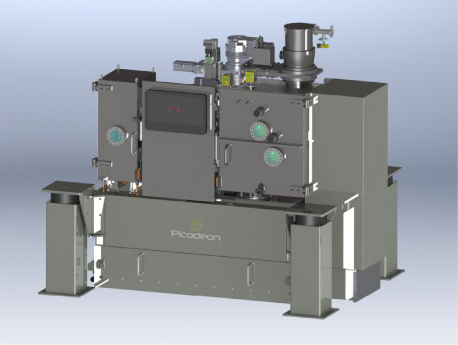
Figure 5. A 3D solid model of a multi-chamber picosecond PLD system currently under construction by PVD Products, Inc. for Picodeon Oy. This system includes a loadlock with elevator for handling ten wafers for substrates up to 150 mm in diameter or 100 × 100 mm2 in size, a robotic wafer handler, a pre-clean chamber using heating and a low-energy argon ion source, and a main deposition chamber. The deposition chamber features multi-target capability, a high-speed scanning method using their patented cold ablation process to quickly create stoichiometric thin films. Photo courtesy of Picodeon Oy.
Download figure:
Standard image High-resolution imageFigure 5 shows a 3D solid model of a large-area picosecond PLD system currently under construction. This system handles wafers up to 150 mm in diameter with a 10 position loadlock, Brooks robot handler and chamber, wafer pre-clean chamber and deposition chamber.
Figure 6 shows a photograph of a typical commercially available PLD system for R&D applications. This system can handle 50 mm diameter wafers and includes a target manipulator with six 50 mm diameter targets, a dual-position loadlock, HP RHEED, programmable target-to-substrate distance, and two ultra-high vacuum (UHV) magnetron sputtering sources along with a high-temperature non-contact heater. Several similar PLD systems are available from the other vendors mentioned above and are shown in the online supplementary data (stacks.iop.org/JPhysD/47/034005/mmedia).
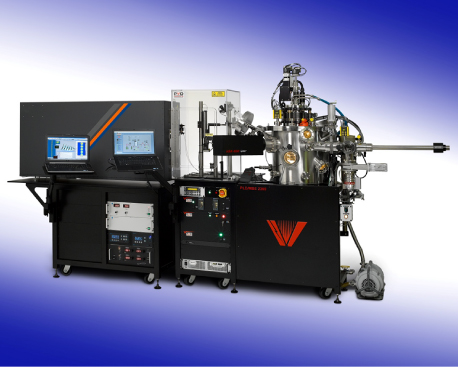
Figure 6. Photo of a commercial PLD/MBE-2300 system. The system includes a six-position 50 mm diameter target carousel, 50 mm diameter substrate holder with heating to 950 °C, two UHV magnetron sputter sources, HP RHEED, a dual wafer loadlock and a base pressure below 5 × 10⁻⁹ Torr. Photo courtesy of PVD Products, Inc.
Download figure:
Standard image High-resolution imageAll of the systems shown in the online supplementary data as well as that shown in figure 6 are capable of multi-layer and epitaxial film growth of very high quality films. As an example figure 7 is a photograph of a Nb-doped (1% of the B-Site) SrTiO3 epilayer grown on a (0 0 1) SrTiO3 substrate by the Rothschild group at Technion, Israel Institute of Technology. The film was grown at 800 °C in 1 mTorr of oxygen with a laser fluence of 1 J cm−2 at a frequency of 3 Hz. Target-to-substrate distance was set at 60 mm [17].

Figure 7. High-resolution TEM photograph of a Nb-doped SrTiO3 film grown on a (0 0 1) SrTiO3 substrate. Photo courtesy of Technion Israel Institute of Technology.
Download figure:
Standard image High-resolution imageMAPLE, a variant of PLD, was developed by the group at Naval Research Labs in the late 1990s by Doug Chrisey, Alberto Piqué, Jim Horowitz and Andrew McGill [4]. This laser process has been developed to deposit polymer films of various types onto a variety of substrates [4]. Direct deposition of polymer films using excimer-based PLD typically destroys the polymer structure due to the high energy of the UV photons. For the MAPLE process the desired polymer to be deposited is typically dissolved in an appropriate solvent. The amount of polymer would be typically ∼2% or less. The polymer/solvent (P/S) mix is then injected into a cup within a purged vacuum chamber back filled to a pressure close to atmosphere with dry nitrogen or argon. The cup is typically surrounded by a copper housing that is filled with liquid nitrogen after the P/S injection. The P/S mix is then frozen in place and the chamber pumped down. Under ideal conditions using a pulsed laser the solvent will absorb the laser radiation and evaporate in a few µs. The evaporation process throws the polymer and solvent into the vapour phase. The polymer is then transferred and condensed onto a substrate (usually held at or near room temperature) while the solvent is pumped away. Typically lasers with long wavelengths are desirable for the MAPLE process as the energy of excimer photons are on the order of 5.4 eV at 248 nm. This energy is sufficient to break the polymer chains thus destroying the functionality desired from the polymer in the thin film. The best choice of laser to use for this process is ones with a long wavelength such as the Nd : YAG or Er : YAG that operates at 1.064 µm (∼1 eV/photon) and 2.92 µm (∼0.3 eV/photon) [18]. A Q-switched Nd : YAG laser has pulse lengths which are on the order of 10 ns. On the other hand, the Er : YAG laser has fairly long pulse length (∼150 µs) as it is difficult to Q-switch. Also, RIRPLE [4] is yet another variant of the laser deposition process [4] developed by some of the NRL team including Danny Bubb along with Richard Haglund from Vanderbilt University where they have a small free electron laser. In this case, one tries to tune the laser wavelength to a vibrational band of the polymer material to excite and evaporate material. It is interesting to note that water strongly absorbs radiation at 2.94 µm making this 'solvent' an excellent choice for a RIRPLE MAPLE process.
As an example of some MAPLE work that has been recently conducted figure 8 is photograph of a film of poly(3-hexylthiophene) (P3HT), a conductive polymer, deposited onto a 100 mm diameter wafer in a RIR MAPLE system similar to that shown in figure 9. This work was conducted at Duke University by the Adrienne Stiff-Roberts group. The system was designed to handle 50 mm diameter wafers and typical deposition conditions have been previously published [19]. However, the system was adapted by the end user to handle 100 mm diameter wafers and the film thickness profile of a 350 kDa polystyrene film deposited by RIR MAPLE is shown in figure 10. Grid marks etched into this wafer were used to measure the film thickness profile. At the largest target-to-substrate distance of 7 cm, the film thickness is uniform across an approximately 50 mm diameter area of the substrate. As the substrate is moved closer to the target, the deposition becomes more peaked in the centre of the substrate, as expected, and the deposition rate increases substantially. This is the first published data of film thickness for the MAPLE process to the author's knowledge. These films were grown with a laser repetition rate of 2 Hz, laser power of 2 J cm−2. At a target-to-substrate distance of 7 cm the growth rate was ∼33 nm h−1. Such slow growth rates are related to the low laser power as well as small concentration of the polymer within the P/S mix.
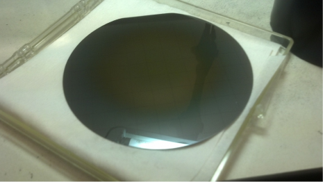
Figure 8. Photograph of a 350 kDa polystyrene film deposited onto a 100 mm diameter substrate with a RIR MAPLE technique using a system similar to that shown in figure 9. This work was conducted by the Stiff-Roberts group at Duke University.
Download figure:
Standard image High-resolution image
Figure 9. Photograph of a RIRPLE/MAPLE deposition system. These systems are typically set up for 50 mm diameter wafers and can handle from one to four MAPLE targets. Photo courtesy of PVD Products, Inc.
Download figure:
Standard image High-resolution image
Figure 10. Film thickness profile of 350 kDa polystyrene films grown by the RIR MAPLE process on a 100 mm diameter substrate at Duke University by the Stiff-Roberts group. The average measured film thickness as a function of radial distance from the wafer centre for four target-to-substrate distances ranging from 4 to 7 cm is shown. In addition to averaging three separate measurements at each location, the same radial distance at four different locations are averaged together to generate this graph.
Download figure:
Standard image High-resolution imageFigure 9 shows a RIRPLE/MAPLE system that utilizes a commercial Nd : YAG laser with an OPO. The OPO provides radiation from about 700 nm out to about 2.5 µm. This laser has peak energy of about 100 mJ at 700 nm and drops off to about 15 mJ at 2.5 µm. The system is currently being used for deposition of biological materials. It is fully computer controlled and load locked.
Figure 11 shows a photograph of a unique multi-target MAPLE/RIRPLD target assembly made for the FEL at Jefferson Laboratory [18]. This unit is liquid nitrogen cooled and holds six targets which can be exchanged from six P/S mixes to six solid polymers for RIRPLD. The set up shown is for three targets of each type.
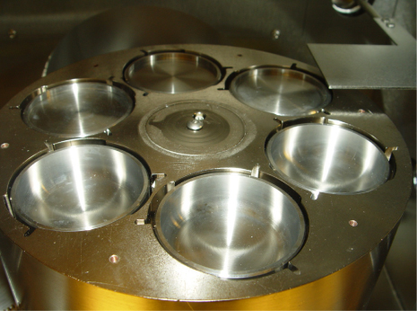
Figure 11. Photograph of a multi-target MAPLE/RIRPLD liquid nitrogen cooled stage, shown with three MAPLE cup holders for P/S mixes, and three solid target holders. Photo courtesy of PVD Products, Inc.
Download figure:
Standard image High-resolution imageMAPLE, RIR MAPLE and RIRPLE are still far behind in both sales volume and equipment development compared to that of standard PLD. However, these are very interesting techniques especially for the growth of polymer films. It is felt that if a pulsed tunable laser in the range from 1 to ∼5 µm with a pulse length of ∼1–100 ns and power of ∼1–20 W were commercially available this would be a great enabler for growth of a wide variety of polymer films. Unfortunately such lasers are currently not available at a price researchers can afford. IR tunable lasers are commercially available but with much lower power levels in this wavelength range.
Almost all of the vendors noted above offer small-area systems (1 cm2 to 50 mm in diameter) with multiple targets, high-temperature heaters, loadlocks, software, either laser beam rastering or target toggling (or both), HP RHEED, ellipsometry, emission spectroscopy, various types of pulsed lasers, etc. Modern PLD systems now also can include other PVD devices such as pulsed electron deposition (a technique similar to that of PLD and provided by Neocera) [20, 21], magnetron sputtering sources [22], effusion cells, ion sources [23], atom sources [24–26], ECR sources [27] and ozone generators [28, 29].
Figures 12 and 13 are photographs of the insides of two different PLD systems that contain some of these devices.

Figure 12. Photograph of the internal view of a PLD/MBE-2500 system that includes six 2 inch PLD targets (one seen through the slot in a water-cooled circular plate), five effusion cells, and a Staib high-pressure re-entrant RHEED gun and RHEED screen. Photo courtesy of PVD Products, Inc.
Download figure:
Standard image High-resolution image
Figure 13. The internal view of a PLD/MBE-2300 system with six 2 inch diameter targets with a UHV magnetron sputter source and a Kaufmann dc ion source. Photo courtesy of PVD Products, Inc.
Download figure:
Standard image High-resolution image5. Production PLD equipment
Larger area PLD systems have been commercially available for over 15 years. Figure 14 shows a more modern version of a large-area PLD-5000 system that handles 125 mm diameter substrates or multiple 50 mm diameter substrates. This system includes four 100 mm diameter targets, a large-diameter Intelligent Window, constant-focus laser beam rastering package [4], a blackbody substrate heater that heats Si to 950 °C [13], variable target-to-substrate distance and a loadlock. The excimer laser (typically an 80 W laser) would be mounted on a table next to the optical train enclosure seen on the left side of the machine. With this laser the system can deposit most oxides at rates of 2–5 µm h−1 over a 125 mm diameter substrate. Figure 15 shows a photograph of a commercial load-locked PLD system for 200 mm diameter wafers with heating to 750 °C offered by Neocera.
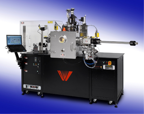
Figure 14. Photograph of a PLD-5000 system that handles 125 mm diameter or multiple smaller wafers. Photo courtesy of PVD Products, Inc.
Download figure:
Standard image High-resolution image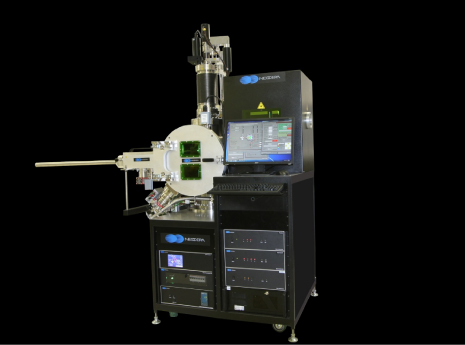
Figure 15. A photograph of a Pioneer 200 large-area PLD system to handle 200 mm diameter wafers, loadlock with substrate heating to 750 °C. Ports are provided on the chamber to add other components. Photo courtesy of Neocera, LLC.
Download figure:
Standard image High-resolution imageFigure 5 shown above is a production tool currently being fabricated by PVD Products for Picodeon using picoseconds laser technology. This system can handle ten wafers in the loadlock up to 6 inch in diameter and will be installed in January 2014.
Interest in high-temperature superconducting CCs also has pushed the limits of PLD technology. One of the significant issues in the early days of PLD for CC technology was that the laser plume would start to tilt back towards the laser after very long depositions even on large-diameter targets. Laser plume tilting caused by laser-induced microstructure on the target is a well-known phenomenon [3, 4]. A solution to deal with this issue was the development of the XYΘ target manipulator by PVD Products [4]. This manipulator is designed so that the laser beam will hit each spot on the target surface from a full 360° over time, thus significantly reducing cone formation and eliminating plume tilting. Such target manipulators are requirements for CC applications and can be used in standard large-area PLD tools with relatively smaller diameter targets with proper software and laser beam rastering control.
As an example figure 16 shows a photograph of an internal view of a large-area PLD tool that is connected to a FOUP that holds twenty-five 300 mm diameter wafers and integrated with a robotic wafer handler and chamber and PLD chamber. The PLD chamber includes a substrate heater to 300 °C, a four-position XYΘ target manipulator with 100 mm diameter targets, large Intelligent Window, constant-fluence laser beam rastering, a multi-pocket electron beam evaporation source, Coherent LPX Pro 220i 80 W excimer laser and full computer control.

Figure 16. Photograph of the internal portion of a 300 mm capable PLD system that includes a four-position XYΘ target manipulator with 100 mm diameter targets, constant-fluence optics train, substrate heater and electron beam evaporation source. Photo courtesy of PVD Products, Inc.
Download figure:
Standard image High-resolution imageAnother example of large-area PLD equipment has been driven by the need for lead zirconate titanate (PZT) materials for microelectromechanical system (MEMS) applications. Figure 17 shows a photograph of a Piezo-Flare-800 PLD system specifically designed to development and production of PZT material and other oxide based compounds. This system includes the capability to grow uniform high-quality films onto substrates as large as 200 mm, with a high-temperature substrate heater, particle reduction filter, multi-target manipulator, laser beam homogenizer and attenuators. Typical growth rates between 1.8 and 3.6 µm h−1 are achievable with this system and about 80 W. The Piezo-Flare has a competitive low cost of ownership as well. Some photos of PZT films grown in such equipment are shown in figure 18.
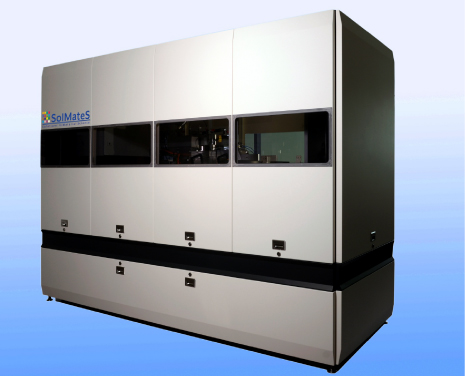
Figure 17. Photograph of a Piezo-Flare 800 system. This system can handle wafers up to 200 mm in diameter and is specifically designed for PZT deposition for MEMS applications. It includes wafer heating up to 800 °C, a thickness non-uniformity spec of <3% typical, particle filter, fully automated with SEMI compatible fab interface software, integrated laser with homogenizer and beam attenuator. It is available with cassette-to-cassette loading via robotic chamber. Photo courtesy of SolMateS B.V.
Download figure:
Standard image High-resolution image
Figure 18. Photograph of a homogeneous 200 mm diameter PZT film deposited on Si/Pt 200 mm diameter wafer. Also a photo of a patterned 150 mm diameter wafer with patterned test structures for 31 measurements. Photo courtesy of SolMateS B.V.
Download figure:
Standard image High-resolution imageAs a final example of production-oriented PLD equipment, shown in figure 19 is a PLD reel-to-reel tool for the growth of YBCO onto CC tapes using a Coherent Lambda Steel SX300K 300 W excimer laser operating at 248 nm. This tool utilizes a large XYΘ target manipulator with a single 300 mm diameter YBCO target, multi-plume (up to 12 plumes) and multi-roll technology (up to 28 rolls), and a blackbody heater that heats the tape to 850 °C at tape speeds of over 200 m h−1 [4, 13]. The tape speed and tension as well as temperature and deposition pressure are all controlled via closed-loop feedback systems. The diameter of Intelligent Window disc used is 740 mm and requires special tooling to handle the large disc. This window not only rotates around its central axis but also slides laterally to make use of ∼85% of the entire disc area, not just the outer edge of the disc. The tool is designed to deposit thin CeO2 materials and between 1 and 2 µm of epitaxial YBCO onto metal SS, Hasteloy, or RABiTs tapes 1 cm wide and 1 km in length and about 50 µm thick. The effective surface area of this tape is 10 m2. This is equivalent to coating 105 1 cm2 samples in one run which may take between 5 and 10 h depending on the desired film thickness (typically between 1 and 2 µm). Clearly PLD has come a long way from its humble small area beginning in 1987.

Figure 19. Photograph of a commercial reel-to-reel PLD tool capable of depositing CeO2 or LaMnO3 buffer layers and micrometre thick YBCO films over 1 cm wide by 1 km long Hasteloy tapes. The total effective area of such a tape is 10 m2. Photo courtesy of PVD Products, Inc.
Download figure:
Standard image High-resolution imageResults grown in these large-area reel-to-reel systems have been very encouraging. Both very long lengths of tape and high currents have been achieved. Work conducted within six months of receiving a previous version of this type of reel-to-reel tool delivered to SRL/ISTEC in Japan in 2005 yielded tapes that were 212 m in length and 1 cm wide with a current carrying capability of 245 A. The growth rates were 3.7 m h−1 for films about 1.5 µm thick using five lanes of tape and about 160 W. This result set the figure of merit for the product of length and current for CC technology for several months. Shorter lengths of 1 cm wide CC tape displayed currents of over 500 A.
Figure 20 shows the XRD Θ–2Θ scan of a YBCO film deposited onto a CeO2 buffer layer deposited onto a Hasteloy CC tape at Shanghai Jiao Tong University. Both films were deposited by PLD in a PVD Products reel-to-reel tool [31]. Figure 21 shows the voltage/current capability of such a piece of HTS tape 100 m in length. The results indicate currents of 270 A are readily achievable via this technique [30].

Figure 20. XRD of YBCO and CeO2 films deposited onto a Hasteloy tape via PLD in a reel-to-reel tool.
Download figure:
Standard image High-resolution image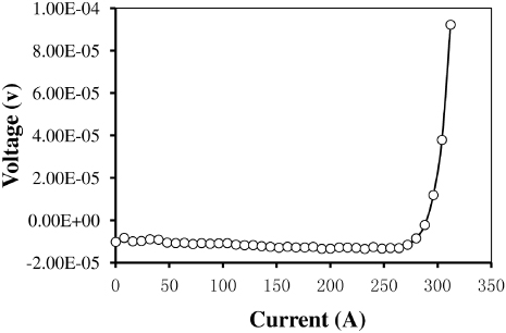
Figure 21. The voltage/current characteristic of a 100 m length of 1 cm wide tape with a 1.5 µm thick YBCO film deposited on CeO2 buffer layer both deposited onto a Hasteloy tape via PLD in a reel-to-reel system.
Download figure:
Standard image High-resolution image
6. Conclusions
It is interesting to note that unit sales of excimer lasers have been fluctuating over the past five years but are fairly flat on average. While the exact number is not readily available, Coherent, the dominant supplier of excimer lasers for PLD, sells between 60 and 100 lasers a year for PLD. However, there is a definite trend in increasing sales of higher power lasers such as the LPX Pro with 50+ W, LEAP lasers with 100+ W, and LSX lasers with 300–540 W of power. This is a direct indication that both the HTS coated-conductor as well as large-area wafer based electronics markets are growing for PLD. It is expected that MAPLE and RIRPLE will also expand over time, especially if new long wavelength lasers can be developed with higher power and short pulse lengths to help enable these techniques.
It is surprising that the market for commercial PLD equipment keeps on growing. I expected that the PLD market would have stagnated at some point around 2000 when everyone who wanted a PLD tool would have purchased or built one. However, commercial PLD tool sales and the market continue to expand at a remarkable pace driven by the ever-expanding need for new material structures. The complexity and costs of modern PLD machines also continue to expand as well to meet these demands. Large-area PLD applications for MEMS and coated conductors have already been demonstrated. It should also be pointed out that PLD is a low-temperature process when compared to other PVD techniques and can be used on temperature sensitive substrates [32]. Thus, applications such as flexible substrates for displays, solar cells, batteries, etc are possible areas of expansion for this process.
Twenty-five years after its re-incarnation PLD activity is still going strong. This discussion does not focus on the growing interest in picosecond and femtosecond lasers noted above and these are active areas of research as well. The future for growth in PLD looks bright. Soon all laboratories involved in thin-film deposition will have at least one PLD tool at their disposal. Production machines are currently being delivered for various applications and this trend will definitely continue. This demand will drive systems to larger substrate sizes, with more interesting capabilities thus enabling new applications for this unique physical vapour deposition process.