
Abstract
In this work we present a two-dimensional (2D) model for an organic thin film photo-conductive sensor containing a planar heterojunction and in-plane electrodes. The model simulates the flow of charge carriers based on the standard one-dimensional semiconductor transport and continuity equations, and combines this with a 2D model for the electric field. This procedure results in a hybrid differential/integral equation formulation. We present and analyse simulation results that resemble very well measured current–voltage characteristics of a real sensor under different illumination levels. We find that for currents below a critical value the sensor behaves like a resistor. Above this critical current the current increases much more slowly due to space charge accumulation close to the cathode. We explain the critical current as the maximum reverse current of the solar cell formed by the heterojunction covering the cathodic electrode.
Export citation and abstract BibTeX RIS
1. Introduction
Organic electronic devices are slowly replacing conventional inorganic ones, especially in applications where properties like transparency and flexibility are desired. The simulation of novel organic electronic components offers insight into the working principle of the device and the behaviour of charge carriers, and can help to reduce the time needed for the design, testing and development of new components.
The modelling of organic electronic devices is a challenging domain. The behaviour of organic semiconductors is related to that of inorganic semiconductors, but there are a few fundamental differences. The transport of charge carriers for example occurs via hopping [1] instead of via a Fermi gas, and energy levels are defined by molecular orbitals rather than by conduction and valence bands in a crystal. In the literature we find articles which describe the modelling of organic light emitting diodes (OLEDs) [2] and of organic thin film transistors (OTFTs) [3, 4]. The modelling of OTFT's is often based on the thin film transistor (TFT) theory of their inorganic counterpart [5–7].
In this paper we present a model for an organic photo-conductive sensor similar to a device which was initially presented by Ho J C et al [8] as an 'in-plane organic bilayer heterojunction photoconductor' (see figure 1). Since our aim is the fabrication of a transparent sensor, the main modification of our device is the use of indium tin oxide (ITO as electrode material instead of gold. The sensor consists of a hole transport layer (HTL, e.g. m-MTDAB) and an exciton generation layer (EGL, e.g. 3,4,9,10 perylenetetracarboxylic bisbenzimidazole (PTCBI)) deposited on top of two interdigitated ITO electrodes. The ITO electrodes and the HTL are highly transparent (95%), while the EGL absorbs a rather small fraction of the incident light. A photon that is absorbed by the EGL forms an exciton, which can diffuse in the EGL. Due to the high binding energy of the exciton in PTCBI (EB = 0.20 ± 0.03 eV [9, 10]) it is unlikely that spontaneous dissociation into free charge carriers occurs. If an exciton reaches the EGL/HTL interface, it can transform into a charge transfer (CT) state [11]. The CT state occurs when the hole of the exciton is captured by the highest occupied molecular orbital (HOMO) of the HTL and the electron by the lowest unoccupied molecular orbital (LUMO) of the EGL, while the electron and hole remain bound across the interface via Coulomb forces. Note that the probability for the CT state to dissociate into free charge carriers is close to unity [12, 13]. After dissociation, the electron and the hole are located in respectively the EGL and the HTL. The charge carriers drift under influence of a field and or diffuse and contribute to the conductivity of the organic photoconductor (OPC) sensor.

Figure 1. (a) Architecture of the organic transparent photo-conductive sensor. Cross-section perpendicular to the ITO electrodes; (b) illustration of the interdigitated electrode pattern.
Download figure:
Standard image High-resolution imageIn a previous paper [13] we presented the fabrication and the electro-optical characterization of the OPC in detail. Typical J(V)-curves obtained for a range of illuminances are shown in figure 2 for a device with a bilayer made of 40 nm m-MTDAB and 10 nm of PTCBI. For low voltages the current increases linearly with the voltage up to a threshold at which point the characteristic switches to a still almost linear curve but with a much smaller slope. Somewhat similar characteristics were obtained by Lombardo et al [14] for a lateral organic bulk heterojunction device, although their characteristics are clearly non-linear for V → 0. Besides asymmetrical Au/Al contacts their device has only one active layer, a 220 nm thick P3HT : PCBM blend, and is fabricated on Si/SiO2, which serves as gate electrode. In a subsequent paper Ooi et al [15] attributed the shape of these J(V)-characteristics to space-charge limited extraction of photo carriers and presented some modelling to prove this point. No simulations of J(V)-curves were included however. In his thesis Ho J C [16] suggested already that space-charge is the cause for the shape of the J(V)-curves, but without actually modelling the behaviour. In previous papers we also pointed to space-charge as the main cause and revealed the presence of the space-charge near the cathode by a local illumination experiment [17, 18].
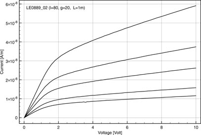
Figure 2. J(V)-curves for a typical bilayer sensor made of 40 nm m-MTDAB and 10 nm PTCBI for different illuminances Φ = 373, 180, 104, 47 and 29 cd/m2. The sample was illuminated with the backlight of a LC-display. The sensor is made of fingers with width 80 µm and a gap of 20 µm and the total gap length equals 1 m.
Download figure:
Standard image High-resolution image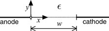
Figure 3. Coordinate system used for simulating the gap.
Download figure:
Standard image High-resolution imageIn order to better understand the measured J(V)-characteristics we developed a numerical model which solves the standard semiconductor equations and the Poisson equation in the gap between the electrodes. Considering the large difference between the thickness of the bilayer (50 nm) and the width of the gap (20 μm in the example shown in figure 2 but we did also measure samples with a gap width of 6 μm), we treat the transport/continuity equations as one-dimensional (1D), meaning that the bilayer is modelled as an infinitesimally thin sheet. However, contrary to the analysis given in [15] we feel that given the planar geometry of the electrodes and the absence of a gate electrode,the calculation of the electric field must be done in two dimensions. Although a purely 1D model might show similar qualitative (space-charge related) behaviour, the rapid increase of the electric field near the electrodes cannot be neglected. Moreover we will show that the electric field can be calculated two-dimensionally (2D) without performing a full blown 2D numerical calculation.
As already noted there is fair agreement that the specific shape of the J(V)-curves is caused by a space-charge effect. However as far as we know no one has explained at what point of the characteristic this space-charge effect comes into play. Experimenting with our simulation model, we have found that the knee in the characteristic occurs when the current reaches a critical value, which in our devices is set by the part of the sensor located above the cathode. This effect is taken into account via the boundary conditions for the electron transport/continuity equations. In fact it is clear that the HTL/EGL bilayer forms a solar cell heterojunction diode which is forward polarized above the anode and reversely polarized above the cathode and the critical current is equal to the saturation current of this reversely biased solar cell.
The rest of the paper is organized as follows. In section 2, we give a description of the simulation model used in the gap, in particular of the solution for the field problem. The electron boundary condition and the behaviour of the solar cell above the electrodes are treated in section 3 and in section 4 the model is applied to the device illustrated in figure 2.
2. The gap model
2.1. The differential equations
The photo-conductive sensor has an in-plane architecture. It consists of two interdigitated electrodes on a glass substrate and covers an area of approximately 1.0 × 1.0 cm2. The interdigitated electrodes are coated with a stack of organic materials. The width of the individual electrode fingers, and of the gap between two adjacent fingers are in the order of tens of micrometer, which is much smaller than the length of the fingers (10 mm). If we neglect the boundary effects at the tips of the electrode fingers, we can model the sensor with a 2D model for a single pair of electrodes with a length equal to the total effective length of the interdigitated electrodes.
The organic stack and the ITO electrodes are a few tens of nanometre thick, which is negligible compared to the lateral dimensions of the device. Therefore we treat the bilayer within the gap and the electrodes as infinitesimally thin sheets. The electrodes are assumed to be perfect conductors. We choose the x-axis in the gap with the origin x = 0 situated at the tip of the anodic electrode (see figure 3). The cathodic tip then corresponds with x = w, w being the width of the gap.
The sheet is characterized by surface carrier densities ps(x) and ns(x) with unit m−2 and carries a corresponding surface charge density πs(x) = q[ps(x) − ns(x)], where q is the electronic charge. Note that in our bilayer device the holes and electrons are situated in separate HTL/EGL layers but the same model can be applied to a bulk heterojunction device.
The electric field E = Ex in the 2D system is a superposition of the applied field Ea(x), which is due to the voltage applied between the electrodes without charge being present in the gap, and of the (in-plane component of the) field Eπ(x), which is due to the surface charge density πs(x) with short-circuited electrodes. Using superposition the latter field can be obtained by considering the field due to a line charge situated at an arbitrary position x' within the gap. For the 2D lay-out considered with infinitely thin electrodes (left electrode at potential V, right electrode grounded), the fields in the organic layer (on the x-axis) can be obtained analytically by a conformal transformation [19–21], assuming the electrodes are embedded in a medium with a uniform dielectric constant  . Considering that our sensor is placed between two glass plates the latter is an acceptable simplification and calculations have been done with = 30. The problem then reduces to solving the Laplace equation with the proper boundary conditions. In two dimensions the solutions of the Laplace equation are harmonic functions, which can be used to define a complex potential. This complex potential can be transformed using a complex conformal transformation z' = f(z) and in this way the solution for a simple geometry can be transformed into the solution belonging to a much more complicated geometry. In our specific case the geometry with two semi-infinite electrodes separated by a gap can be transformed into the much simpler geometry of two semi-infinite electrodes without a gap. In the latter case the equipotential lines are radial straight lines and the field lines are semi-circular arcs. Transforming this solution back to the original geometry we obtain both field components defined higher:

where w is the width of the gap between the electrodes and

where G(x, x') is the 2D Green's function:
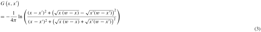
G(x, x') gives the normalized potential at x due to a line charge located at x'. In these formulas it is assumed that the electrodes are semi-infinite. If desired the finite width of the electrodes can be taken into account with some added complexity. In the numerical implementation we actually use the electric potential in the sheet φ(x), which is given by:

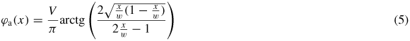
where the first contribution is due to the applied potential:
Introducing the Slotboom variables
 and
and
 , with Vth = kBT/q the thermal voltage (kB is the Boltzmann constant and T the temperature of the layer in Kelvin), the surface current densities for the electrons and holes (unit m−1s−1) are written as:


where Dn/p are the charge carrier diffusion coefficients, which are calculated with the Einstein-Smoluchowski equation D = μVth, with μn/p the charge carrier mobilities. For the diffusion constants in equations (6) and (7) we use the electron diffusion constant Dn of the EGL and the hole diffusion constant Dp of the HTL.
The conservation of charge in the organic stack is described by the continuity equations, which are written as:

where g(x) is the local surface generation rate of electrons/holes due to exciton dissociation and r(ns, ps) the surface recombination rate, both expressed in m−2 s−1. In what follows only a uniform generation rate will be considered.
2.2. Boundary conditions
The transport equations must be complemented with boundary conditions, which depend on the contact properties between the ITO electrodes and the organic stack. Since the HTL layer is in direct contact with the ITO the boundary condition for the holes is straightforward. Based on detailed balance and Poole–Frenkel field emission the following simplified expression can be used for the hole current at the anode (a similar condition is applied at the cathode for x = w) [22]:

where ps0 is the hole surface density in equilibrium, Ee(0) ⩾ 0 the effective electric field at the ITO/HTL interface, E0 a reference field
 , Sp the hole interface recombination velocity and ps(0) the hole surface density at the interface. For a negative field Ee(0) ⩽ 0, the exponential factor must be replaced by 1. The barrier height is included in the factor Spps0. For the ITO/HTL interface we expect an injecting contact, due to the small energy barrier between the HOMO of HTL (below −5 eV [23, 24]) and the work function of the ITO (estimated between −4.3 eV and −4.7 eV [25]). Electrons are not injected into the HTL due to the high barrier with the LUMO of the HTL (≈ −2 eV). Due to the planar approximation used in (1) the electric field near the anode tends to infinity as
 and therefore we use an effective field in (9) obtained by averaging E(x) over a distance equal to the approximate thickness t of the ITO electrode:

For the electrons the situation is more complex since the EGL layer is not directly in contact with any electrode. This problem will be treated more thoroughly in section 3 but here we already look at the situation at the anode. Due to the applied electric field photo electrons generated in the EGL will be driven towards the anode. These electrons will induce a positive image charge in the anode which in turn results into hole emission from the anode through the Poole–Frenkel effect already described. Finally at the HTL/EGL interface the holes emitted by the anode will recombine with the piled up electrons. Therefore we accept that through this mechanism the anode forms a relatively good sink for the electrons which could be described in a simple way by introducing a recombination velocity Sn and a boundary condition of the form:

where ns0 is a constant, which is relevant for the behaviour at the cathode.
2.3. Numerical implementation
The equations (4),(6),(7) and (8) form a hybrid differential/integral equation system which must be solved in the gap (0 < x < w) for the potential φ(x), and the carrier densities ps(x) and ns(x). Following Selberherr [26], we discretize the differential equations using the finite difference (FD) method, and solve the discretized equations following the standard Scharfetter–Gummel scheme [27, 28]. The gap is divided into N elements with variable width and within each discrete element the unknown functions are approximated by a first order polynomial. The same linear approximation is used for evaluating the integral in (4).
According to the Gummel scheme the equation for the potential (4) and the transport/continuity equations are solved iteratively until convergence is obtained. After insertion of the Slotboom variables the equation for the potential becomes:

where it's important to take into account the dependence on the unknown potential in the rhs. Basically this equation is solved for φ given the previous values for us(x) and vs(x). This new potential is then used to solve the transport/continuity equations and to obtain updated values for the carrier densities, where the non-linear recombination term in (8) is linearized. The convergence of the iterative process is tested based on two criteria: the uniformity of the total current density J = q[Jsp(x) − Jsn(x)], and the invariance of the charge carrier densities ns(x) and ps(x) from one iteration to the next.
3. The electron boundary condition and the solar cell characteristic
Since photo holes generated above an electrode are collected easily by the electrode we expect recombination to be weaker here than within the gap and consequently the carrier densities will be higher than in the gap, meaning that the constant ns0 in (11) should actually be replaced by nsoc ≫ ns0, this being the equilibrium electron density above the electrode, taking illumination into account. Since near the cathode but within the gap the applied field drives the electrons away from the cathode, an electron density gradient is set-up above the cathode which drives the photo electrons towards the gap at the left. A proper boundary condition for the electrons must take into account this current above the cathode. As evidence for this model we mention that our previously published local illumination experiment [17, 18] showed that an incremental photo current is generated also when the laser line was positioned above the cathode. And since a space charge was detected near the cathode only we can also conclude that the mobility of the electrons is (much) higher than that of the holes.
To find a proper boundary condition, the organic layers covering the electrode have been simulated using the standard semiconductor equations together with Poisson's equation. Due to the nearby presence of the electrode there is no need to calculate the field 2D and this problem can be solved using only one-dimensional (1D) equations in the vertical direction, hereby neglecting the hole current density parallel with the electrode (Jpx ≈ 0) and the electron current density perpendicular to the electrode (Jny ≈ 0) (see figure 4).
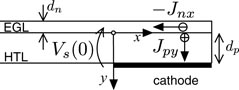
Figure 4. Coordinate systems used for modelling the solar cells covering the electrodes.
Download figure:
Standard image High-resolution image3.1. Vertical solar cell model
In contrast with the gap model where ps takes into account free as well as trapped positive charge carriers, and the effect of the trapped charges is discounted in the (low) values of μp and R0, here both types of carriers are treated separately. As a working model we accept an exponential distribution of traps and assume that free and trapped carriers are in equilibrium with a single Fermi-level. In that case there is a one-to-one correspondence between the free carrier density p and the trapped carrier density pt according to [29, 30]:

where Nv is the effective density of states and Nt an effective total density of trap states. This results into a J(V) characteristic with a dependency
 [29, 30]. We have found evidence for this behaviour in the non-linearity of the J(V) characteristic at the origin for a sample with a 100 nm HTL (see sample S3 in [13]).
Within the HTL the hole transport equation is similar to (7) but now written with mobile volume quantities:

where
 and, due to the absence of bulk recombination, Jpy is constant for 0 < y < dp. Since this holds specifically for mobile carriers we use a different mobility μ'p and diffusion constant D'p. The boundary conditions are given by

at the HTL/EGL interface (y = 0) where g is the same (uniform) generation rate as in the gap and bimolecular recombination is assumed, which will be justified in section 4. At the HTL/electrode interface (y = dp) a condition similar to (9) is applied:

where the exponential must be omitted if Ey(dp) > 0. The Poisson equation is given by:

which is solved with boundary conditions φ(y = dp) = 0 and φ(y = 0) = Vs. Finally we need an expression for the electron interface density n (0) occurring in (15). If we neglect the small component of the electric field perpendicular to the electrode and at the surface of the EGL (Ey(y = −dn) ≈ 0) then −Ey(y = 0) ≈ qns/, where ns is the electron surface density. Since within the EGL we assumed already Jny ≈ 0 and if we assume in addition no trapping of electrons then the electron transport equation and Poisson's equation can be solved analytically [31] and this gives the following result for n(y = 0) as an intrinsic function of ns:


The equations (13)–(19) form a complete set which can be solved numerically for a given voltage Vs. We solved Poisson's equation with the ordinary finite element method and the transport/continuity equation with a mixed finite element method [32]. As a result one obtains the current density Jpy(Vs) and the electron surface density ns(Vs). In practice we first calculate the open-circuit voltage Voc with Jpy(Voc) = 0 and ns(Voc) = nsoc and we then increase/decrease the voltage stepwise to obtain the desired characteristics.
3.2. Model for parallel current
For the electron transport parallel to the electrode surface the EGL is once more treated as a thin sheet and the continuity equation is written as:

whereas the transport equation is given by (6) but is now written as:

where we used the one-to-one correspondence between the potential Vs and ns found in section 3.1. In general (20) and (21) must be solved with the symmetry condition dns/dx = 0 applied in the middle of the electrode and the potential Vs(0) prescribed at the edge of the electrode. However for the present example the width of the electrodes (80 µm) is much larger than the transition region and therefore we integrate (20) and (21) starting with open-circuit conditions Jpy = 0, Vs = Voc and ns = nsoc. We use again a mixed finite element method [32]. In practice we choose the node values Vs, solve the equations in the HTL to obtain ns and calculate progressively the position of the nodes w.r.t. the open-circuit location. Eventually this yields the J(V)-characteristic of the cathode/anode as a relation between −Jnx(0) and Vs(0).
4. Combined numerical model
Both models described in sections 2 and 3 have been implemented in MATLAB. The gap model was solved using 100 variable elements whereas for the solar cell characteristic 25 uniform elements were sufficient. Figure 5 shows the result of a simulation matching the measurements shown in figure 2, where parameters were chosen to obtain a reasonable fit but without actually performing a numerical optimization. In what follows we fill in the missing details and comment on the choice of the chosen parameters.
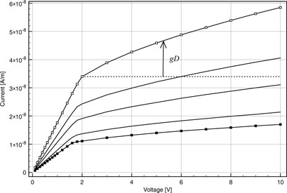
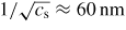
Figure 5. Simulated J(V)-curves matching the measurements in figure 2. Choice of parameters used are discussed in the text. Above the knee the increase of the current is due to the collection of photo generated carriers in the space charge near the cathode (D is the width of the space charge region). The carrier densities and current densities for the highest illuminance and bias voltage are shown in figure 8.
Download figure:
Standard image High-resolution imageBelow the knee in the characteristic the device behaves almost as a perfect linear photo resistor and in this regime the current is well described by:

where due to charge neutrality cs = ps ≈ ns (in reality there is a small space charge to compensate the non-uniformity of the applied field Ea(x) in (1)). We did check relation (22) using sensors with different gap widths. The carrier density cs can be obtained from the uniformity of the current densities in (8) since then:

However the generation rate (of electron-hole pairs) is unknown. In order to obtain some information on the generation rate g we measured the decay of the current J(t) when the illumination Φ is abruptly switched off. Just after switch-off the carrier densities will still be uniform and therefore decay according to the continuity equation:

and with (22) we obtain:

showing that by measuring the slope of this current decay just after switch-off and for different illuminations Φ we obtain the dependence of g on Φ. In figure 6 the steady-state current before switch-off and the initial slope of the current after switch-off are shown for the device in figure 2 under 639.6 nm laser illumination. Comparing the slopes of the two curves at the high end of the irradiance scale we find that
 and therefore we use the bimolecular recombination law:

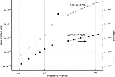
Figure 6. The steady-state current before and the slope of the current decay just after switching off the laser for a range of irradiances. The experiment was performed on the sample shown in figure 2 and with a bias V = 0.5 Volt, which is well within the initial linear region.
Download figure:
Standard image High-resolution imageSince most of the holes in the HTL are assumed to be trapped we choose μp ≪ μn and the linear low voltage behaviour is then defined by the three parameters g, R0 and μn. We choose g = 6 × 10¹⁶ m−2 s−1, R0 = 8 × 10⁻¹³ m2 s−1 and μn = 8 × 10⁻⁹ m2 V−1s−1, where g corresponds with the highest luminance considered (371 cd m−2). The gap carrier density
 (see figure 8 for a complete profile of the carrier densities for V = 10 V). For the other luminances g is obtained by scaling according to the observed Φ0.78 dependence (the values used are mentioned in the caption of figure 7). Based on the spectrum of the backlight used for the measurements in figure 2 we estimate the light contains around 8 × 10¹⁸ photons m−2 s−1 for the maximal illuminance, equivalent with a laser irradiance of 2.5 W m−2. If we also take into account the absorption spectrum of PTCBI then this effective irradiance must be increased slightly to 2.7 W m−2. From the fits shown in figure 6 and the equations (22) and (25) we find that gR0 = 6.4 × 10³Φ0.78. For Φ = 2.7 W m−2 this gives gR0 = 1.4 × 10⁴, whereas for the values selected higher we obtain gR0 = 4.8 × 10³, which is somewhat larger but reasonably close. The other luminances considered in figure 2 then correspond with respectively 1.3, 0.76, 0.34 and 0.21 W m−2 and for the lowest values we can expect some deviation from the accepted dependence Φ0.78, which is visible when comparing figure 5 with figure 2. Finally it must be mentioned that the average in-plane distance between photo carriers
 is rather large compared with the thickness of the layers.

Figure 7. Solar cell J(V) characteristics (top) and J(ns)-characteristics (bottom) of the EGL/HTL heterojunctions covering the electrodes for generation rates g = 1, 0.57, 0.37, 0.20, 0.14 × 6 1016 corresponding with the illuminances considered in figure 2. The characteristics are drawn in the usual way with the forward bias voltage corresponding with −Vs(x = 0) in figure 4 and the current with qJnx(x = 0). The electron surface density ns is the one at the edge of the electrode. The negative currents are relevant for the cathode, the positive ones for the anode.
Download figure:
Standard image High-resolution image
Figure 8. Profile of the surface carrier densities ns, ps (top) and surface current densities Jsn, Jsp (bottom) for electrons (full lines) and holes (broken lines), for the maximum illuminance considered with g = 6 × 10¹⁶ m−2s−1 and for a bias voltage V = 10 V. The gap is located between 0 < x < 20.
Download figure:
Standard image High-resolution image
The J(V) characteristics of the heterojunctions covering the electrodes have been calculated according to the model explained in section 3 and they are shown in figure 7, where the following parameters have been used: the free hole mobility μ'p = 1.3 × 10⁻⁷ m2 V−1 s−1, the equilibrium hole density p0 = 1013 m−3, the surface recombination velocity Sp = 10m s−1, the density of states Nv = 1026 m−3, the effective density of traps Nt = 2 × 1024 m−3, the trap parameter r = 4 and the recombination constant R03 = 3 × 10⁻²⁵ m4s−1. In figure 7 we notice a modest open-circuit voltage Voc≈0.1 in the luminance range considered and a linear behaviour in the neighbourhood of this open-circuit point. The corresponding voltage drop should be added twice to the characteristics in figure 5 (once in the forward direction at the anode and once in the reverse direction at the cathode) but this has not been taken into account and would lead to slightly different parameter values. As already mentioned the characteristics shown in figure 7 become non-linear if the thickness of the HTL is increased and this has been observed in practice.
More important are the J(ns)-characteristics shown in figure 7. We notice that the open-circuit electron density nsoc ≈ 6 − 8 × 10¹⁴ m−2 is higher than the carrier density in the gap (the average horizontal distance between carriers is similar
 and most importantly for ns → 0 the reverse current reaches a limiting value −qJmax. The initial boundary condition (11) needed in the gap model of section 2 has been replaced by a parabolic approximation of the curves in figure 7(bottom) as follows:

where nsoc and Jmax are taken from the calculated curves. Note that the zero argument refers to the gap coordinate system and thus holds for the anode for which ns(0) > nsoc. At the cathode the same boundary condition has been applied but with a sign reversal and with ns(w) < nsoc. Since Jmax is the maximal electron current that can be injected this sets the value of the current at the knee in figure 2. Up to this point the gap behaves simply as a series resistance. Beyond this point a space charge develops near the cathode since more electrons are extracted into the gap than can be replenished by the cathode and the subsequent smaller increase of the current (see illustration in figure 5) is now solely due to the collection of photo generated carriers in this space charge region. In this regime the hole mobility becomes relevant and was chosen as μp = 1.3 × 10⁻¹⁰, where the low value takes into account the trapping. The last parameters needed are those occurring in the hole boundary condition (9) where we used besides Sp = 10 m s−1, already defined higher, ps0 = 4 × 10⁵ m−2, but these values are not really important since injection of holes directly into the gap is negligible.
Finally we want to comment on the compatibility between the parameters used in both submodels. From the observed perfect bimolecular recombination law, which is based on the measurements shown in figure 6, we conclude that in the neutral region of the gap, the carriers are distributed uniformly in the vertical direction and the recombination rate (26) can also be written as:

where f is the fraction of mobile holes and p and n are mobile volume carrier densities. Therefore the recombination constant in (15) was chosen as R03 = R0dpdnf−1. Similarly the hole mobility in the gap and the one used in the solar cell model are related by this same trapping factor μp = fμ'p. For the calculations we estimated the fraction of mobile carriers in the gap as f = 10−3. In the solar cell model where trapped and mobile charges are treated separately we have found that for the trapping parameters used, the mobile holes form only a fraction 2 × 10⁻⁵ of the trapped ones. Maybe a more optimal choice of parameters could bring these two fractions closer.
Table 1. Overview of parameters used in the simulations shown in figures 5–8. dp and dn are the thicknesses of the HTL and EGL and for the fraction of mobile holes in the gap we have used f = 10−3.
| gap model | solar cell model | |
|---|---|---|
| electron mobility | μn = 8 × 10⁻⁹ m2 V−1 s−1 | |
| hole mobility | μp = fμ'p | μ'p = 1.3 × 10⁻⁷m2 V−1 s−1 |
| recombination constant | R0 = 8 × 10⁻¹³m2 s−1 | R03 = R0dpdnf−1 |
| equilibrium hole density | ps0 = p0dp | p0 = 1013m−3 |
| hole recombination velocity | Sp = 10 m s−1 | |
| density of states | Nv = 1026 m−3 | |
| density of traps | Nt = 2 × 1024 m−3 | |
| trap parameter | r = 4 | |
5. Discussion and conclusions
We presented a model which is able to explain the main characteristics observed for an organic in-plane heterojunction photo-conductive sensor. In particular we explained the occurrence of the knee in the J(V)-characteristic. Below the knee the bilayer behaves as a uniform linear photo resistance and for the materials considered, most of the conduction occurs in the EGL, whereas the holes in the HTL remain mostly trapped. On the other hand the bilayer also forms a heterojunction solar cell which operates in open-circuit in the gap, leading to a small voltage difference between both layers, which in itself is not very important. However current must flow from the anode to the EGL through this forward biased solar cell and from the EGL to the cathode through a similar reverse biased solar cell. This reverse current reaches a limiting value when the electron density drops to zero at the edge between the cathode and the gap and this causes the knee in the characteristic. For higher voltages a space charge region develops at the cathode or from an alternative point of view one could say that the reverse biased solar cell above the cathode spreads into the gap. Whereas most of the modelling was 1D we used a 2D model for calculating the electric field in the gap. Due to the planar arrangement of the electrodes the electric field increases sharply close to the cathode and this was taken into account properly by a conformal transformation avoiding a full blown 2D numerical calculation.
We have found a fairly good agreement between characteristics measured and simulated for a range of illuminances. Parameters used in the simulation were based on additional measurements if possible and care was taken to maintain consistency between the parameters used. We believe the parameters used are reasonable values and in particular the mobilities are in agreement with published values. For m-MTDAB we found literature values of μp ≈ 3 × 10⁻⁷ m2 V−1 s−1 [33] and for PTCBI μn ≈ 3 × 10⁻⁸ m2 V−1 s−1 was measured for a FET on SiO2 and higher values after depositing a monolayer [24].
In our current model the vertical dimension is totally neglected within the gap but not in the layers covering the electrodes. This is a good approximation in the middle of the gap and of the electrodes but breaks down in the transition zones between the electrodes and the gap. This results into the steep gradient in the electron density at the anode shown in figure 8(a). This can only be improved by solving all equations in two-dimensions and then also take into account the proper geometry of the electrodes.
Acknowledgments
Part of this work is supported by the TARDIS research & development project funded by the IWT (Institute for the Promotion of Innovation by Science and Technology in Flanders), and by the Interuniversity Attraction Poles program of the Belgian Science Policy Office, under grant IAP P7-35.