

Abstract
This work describes, using mainly transmission electron microscopy as an investigation tool, the nature and behaviour of the crystalline defects which are present in (11-22) semipolar GaN films grown epitaxially on patterned r-sapphire substrates using a 3 step growth process. The microstructure at these different growth stages is described. The independent 3D-crystallites nucleated on the substrate surface contain threading dislocations resulting from the epitaxy on c-sapphire facets and basal stacking faults (BSFs), mainly in the −c-wings. These defects are concentrated in a few hundred nanometre wide stripe-like regions emerging on the top facet of the islands. By a careful choice of the growth conditions, these defective regions may be overgrown by defect-free material, blocking their propagation towards the coalesced surface. However, when the 3D crystals coalesce, new dislocations together with very few BSFs are created at the coalescence boundaries. These coalescence defects propagate to the surface of the films in (0001) planes. In summary, the control of the nucleation and propagation of the crystalline defects allows obtaining large area semipolar films with very low defect densities: 7 × 107 cm−2 for TDs and 70 cm−1 for BSFs.
Export citation and abstract BibTeX RIS
1. Introduction
Most of currently commercialized III-nitride optoelectronic devices are based on heterostructures grown along the [0001] polar direction of the wurtzite structure [1]. Along this orientation, the effects of spontaneous and piezoelectric polarizations are maximal. In the case of InGaN/GaN heterostructures, which are the active parts of both lasers and light emitting diodes emitting in the visible range, the quantum confined Stark effect due to the polarizations discontinuities at interfaces both increases the emission wavelength and reduces the radiative recombination rate due to spatial separation of electron and hole wave-functions. To avoid or at least to reduce these deleterious effects, the growth along nonpolar (c-axis in the growth plane) or semipolar (inclined c-axis) orientations has been developed in recent years [2]. Very good material properties are today obtained with homoepitaxial layers and GaN-based highly efficient optoelectronic devices have already been fabricated. However, the sizes of nonpolar and semipolar GaN substrates remain up to now small and their prices high [3–5]. Therefore, heteroepitaxy on foreign substrates has to be considered. But, heteroepitaxially grown GaN nonpolar and semipolar films contain a high density of structural defects which prevent their use for the fabrication of efficient devices. These defects are mainly basal stacking faults (BSFs) which are terminated by partial dislocations (PDs) or connected to other BSFs by prismatic stacking faults [6]. Different strategies have been developed to reduce the crystalline defects density in such films [7]. One of the most efficient techniques is the growth on patterned substrates. The patterning is conducted in such a way that inclined facets suitable for the growth of polar GaN are revealed [8]. This approach therefore takes advantage of the mastering of polar GaN growth. The resulting GaN orientation depends on the angle between the substrate surface and its inclined facet [9]. Different kinds of substrate have been used as silicon [10] and sapphire [11]. The present study concerns the growth of (11-22) GaN on patterned (10-12) r-sapphire (R-PSS).
(11-22) GaN growth conducted in one step on R-PSS allows an important improvement of crystalline quality as compared to growth on flat unpatterned surfaces [7]. But the density of defects is still too high for the development of efficient devices. We therefore developed a 3 step growth method (3S-PSS) which allows obtaining (11-22) GaN heteroepitaxial films with dislocation densities similar to the best polar GaN films deposited on c-sapphire and a very low BSFs density [12]. The success of such a method is based on the understanding of the behaviour of the crystalline defects. In fact, obtaining low defect density films requires both the control of their nucleation and of their propagation. The purpose of the present paper is to describe the defect management at the different stages of this original growth process using mainly transmission electron microscopy (TEM) as investigation tool.
2. Experimental procedure
The substrate patterning used in our process has been extensively described in previous papers [12, 13]. After the deposition of a 300 nm thick SiO2 layer on the r-sapphire substrate, standard photolithography techniques are used to open 3 μm wide stripes with a period of 10 μm. The stripes are oriented along the [11-20] sapphire direction. The first originality of our approach is to use wet etching in a mixture of H3PO4/H2SO4 (volumic ratio 1/3) to reveal inclined sapphire c-facets. This etching occurs at 270 °C during 30 min. With such a process, smooth-c-sapphire facets are obtained with widths of a few hundreds of nanometres.
The growth of the (11-22) GaN layers is performed by metal organic vapour phase epitaxy using either a homemade reactor (1 inch × 2 inch) or a commercial shower head reactor (3 inch × 2 inch), both presenting a vertical geometry. Trimethylgallium, silane and ammonia were used as precursors for gallium, silicon and nitrogen respectively. The growth parameters are varied between the different growth stages. The nucleation process is similar to the one that is classically used for the growth of polar GaN on c-sapphire: a nitridation of the sapphire surface at 1080 °C, a short exposition to a silane flow, the deposition of a 30 nm thick GaN nucleation layer (NL) at 580 °C and then an annealing at 1080 °C. Then, the first growth process step is initiated at 1100 °C using a reactor pressure of 800 mbar and a V/III ratio of 3500. The second step allows a drastic increase of the growth rate along [0001] relatively to the growth rate in the perpendicular [11-20] direction by choosing the following conditions: a temperature of 1100 °C, a low V/III ratio (500) and a low reactor pressure (100 mbar). Finally, to obtain a continuous and flat film, growth conditions should be changed again in a third step. A temperature of 1080 °C, a V/III ratio of 5000 and a reactor pressure of 100 mbar, ensure a rapid coalescence of the growth islands. To obtain a continuous flat film with the periodic pattern used, a thickness of at least 10 μm should be grown [12].
Cross-sectional (CS) and plane-view (PV) TEM samples were mainly prepared in a classical way by mechanical polishing followed by ion-milling. Some TEM samples have been prepared only by mechanical polishing using wedge-shape geometry. The observations are made with a JEOL 2010F (200 kV) and a TITAN 80–300 (300 kV) microscopes. Figure 1 shows the epitaxial relationships between (11-22)GaN and r-PSS. The horizontal (10-12) r- and inclined (0001) facets of sapphire are represented. In order to reveal all different types of defect, CS observations have been performed along the [1-100]GaN and [2-1-10]GaN orientations. In fact, BSFs are out-of-contrast when observed along the [1-100]GaN zone axis. The plane view observations have been conducted along the [22-43]GaN zone axis. The (22-43)GaN plane is a relatively dense plane and only slightly inclined from the (11-22)GaN plane (6,83° towards (11-20)). All the different types of dislocations and BSFs are in contrast in multibeam images realized along this zone axis.

Figure 1. Schematic representation of the epitaxial relationships between (11-22)GaN and R-PSS. The sapphire axes are in grey and the GaN axes in black.
Download figure:
Standard image High-resolution image3. Defect evolution at the different growth steps
3.1. Nucleation step
The nucleation process is similar to the one used for the growth of polar GaN on c-sapphire. The only difference is the morphology of the starting substrate. In fact, 3 different surfaces are concerned: the inclined c-facet, the top r-facet which is covered by the SiO2 mask and the bottom r-facet obtained after chemical etching. After the annealing, GaN growth does not occur on the SiO2 mask but on both other surfaces. In fact, two GaN orientations are observed (figure 2): semipolar orientation resulting from the polar growth on the inclined c-facet and nonpolar orientation on the bottom r-surface which is expected for the direct growth on planar r-sapphire [14]. But, the annealing step and further growth lead to a preferential polar growth on the c-sapphire facet resulting in the burying of the nonpolar GaN thin film deposited on the bottom r-surface. The (11-22) orientation is the only one observed at the top surface after the deposition of a few hundred nanometres of GaN. Moreover, we did not observe any crystalline defects originating from this underlying nonpolar thin layer.
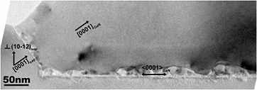
Figure 2. Multibeam CS-TEM image of the GaN/sapphire interface along the [11-20]sapphire zone axis. Both semipolar and nonpolar GaN layers are visible.
Download figure:
Standard image High-resolution imageThe GaN NL is deposited at low temperature (580 °C). It has already been observed that low temperature GaN NL contain a high density of BSFs [15]. In order to observe such BSFs, CS observations along the [2-1-10] zone axis have been conducted. In figure 3, BSFs are clearly observed. Some voids are also sometimes revealed in the NL as in the case of the growth on planar c-sapphire. But the thickness of the buffer layer is low (≈30 nm) and in fact very low as compared to the thickness of the SiO2 mask. Therefore, even if BSFs originating from the NL are in inclined basal c-planes, they are blocked by the SiO2 mask and do not propagate to the sample surface.
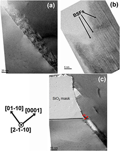
Figure 3. Multibeam CS-TEM image GaN/c-sapphire interface along the [2-1-10]GaN zone axis at different magnifications. BSFs are clearly observed in the NL.
Download figure:
Standard image High-resolution image3.2. Selective growth on c-facet
A selective growth along the +c-direction on the c-sapphire facet is ensured by using the growth conditions described in section 2. After 10 min of growth the shape of the growth islands is trapezoidal with a top (11-22) facet and a very small c-facet (figure 3 in [12]). This morphology may be compared to the one observed in the case of 2 steps epitaxial lateral overgrowth on planar c-sapphire [16]. With a high growth rate along the +c-direction, the nuclei have first a truncated pyramidal section evolving to a perfect pyramidal shape with the gradual disappearance of the c-facet. The behaviour of the defects is drastically influenced by this morphology evolution. In figure 4(a), threading dislocations (TDs) nucleated from the sapphire c-facet are clearly revealed. First, it can be observed that the total number of TDs is limited due to the small width of the c-facet. In fact, reducing the size of the c-facet helps reducing the number of generated TDs [17]. Using chemical wet etching allow obtaining such small c-facets (only a few hundred nanometres large). The TDs first thread along the +c-direction. Then, when they intersect the intersection of the c-facet with the lateral facets, they bend in the basal plane [18–20]. When a pyramidal section is obtained all the TDs have experienced such a process and are in the basal c-plane. This behaviour is represented in figure 4(b), the dashed lines representing the intersecting points between the c-facet and the lateral facets. In figure 4(a), it can be observed that some TDs situated in the centre bend before the ones situated at the edge of the pyramid, in contradiction with the proposed mechanism. In fact, this large pyramid may be the result of the coalescence of smaller ones which may explain this behaviour. After bending, TDs are confined in a stripe corresponding to the lateral facet of the pyramids. TDs bending downwards terminate when they encounter the bottom nonpolar buffer layer whereas TDs bending upwards propagate to the surface. In the case of one step growth on R-PSS these TDs emerge at the surface [7]. It should be noted that the width of the defective stripe is directly related to the width of the c-facet. In the case of (11-22) orientation, the top facet is a (11-22) facet which makes an angle close to 60° (58.41°) with the c-plane. The triangular section is therefore close to be equilateral with a (11-22) facet width nearly equal to the c-facet width. In conclusion, decreasing the width of the c-facet allows both decreasing the number of generated TDs but also decrease the width of the stripe where they are confined after their bending. It should be noted that keeping these conditions allows obtaining nearly defect-free regions in the growth islands (+c-wing) as shown in the right part of figure 4(a).
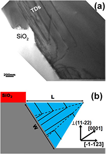
Figure 4. (a) [1-100]GaN zone axis multibeam CS-TEM image of a GaN island grown on c-sapphire facet. TDs bending is clearly evidenced; (b) schematic representation of the TDs bending. The dashed lines represents represent the intersecting points between the c-facet and the lateral facets. The GaN orientation are indicated.
Download figure:
Standard image High-resolution imageTDs are nucleated at the interface between the c-sapphire facet and the GaN islands. There is another source of crystalline defects. In fact, when the growth islands base becomes larger than the sapphire c-facet width and grows above the SiO2 mask, the growth may occur along the −[000-1]-direction (−c-wing). It has been already reported that the growth along that direction results in an important formation of BSFs [21, 22]. This is what is observed in figure 5. Playing with the growth conditions, it is possible to reduce the growth rate along −c and also to reduce the density of BSFs nucleated in the −c-wing [23]. In fact, figure 5 shows an extreme case where the growth conditions enhance the formation of BSFs. Nevertheless, BSFs are always observed in the −c-wings.
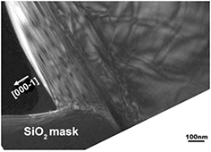
Figure 5. CS-TEM dark field image with  showing BSFs in the −c-wing.
Download figure:
Standard image High-resolution imageAt the surface of islands at the end of this first growth step, highly defective stripe-like regions including the −c-wing and the areas containing the bended TDs alternate with high crystalline quality parts. In the case of one step growth on R-PSS, this microstructure is reproduced up to the surface of the coalesced layers [7].
3.3. Second step: defects blocking
The idea of this second growth step is to play with the growth conditions in order to prohibit the propagation of the crystalline defects to the surface of the final layer. Using the understanding of the initial behaviour of the defects, a process has been developed where the defect-free +c-wing of a crystal overlie the defective region of the adjacent crystal. For that purpose, the growth rate along the +c-direction has to be drastically enhanced relatively to the growth rate in the [11-20] direction. It is obtained by using the conditions described in section 2. A large overlapping is obtained and a void is kept between the two crystals (figure 6(a)). Figure 6(b) is a SEM image of a complete sample grown with a regular introduction of AlN markers (every 1200 s) which appear as dark lines. The distance between these AlN interlayers is larger along [0001] than along both [11-20] and the direction perpendicular to the (11-22) planes. It confirms the higher growth rate along the +c-direction and gives good indication of how the growth front evolves as growth proceeds.
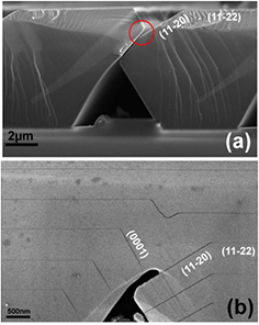
Figure 6. CS-SEM images; (a) at the end of step 2, before coalescence: (b) after coalescence. AlN interlayers (dark contrast) have been introduced to evidence the evolution of the morphology of the growing layer.
Download figure:
Standard image High-resolution imageIn figure 7, it is clearly observed that most of the TDs terminate at the void. BSFs are out-of-contrast along the zone axis used but they also terminate at the void. Only a few TDs escape from this very efficient blocking process (red arrows). The presence of this void is drastically important. In fact, figure 7(b) shows an overlapping where 2 crystals unintentionally touch. The consequence is the propagation of a TD from the defective region of the bottom crystal to the top crystal (blue arrow). At the end of this growth stage, if the overlapping has been correctly driven (presence of a gap between the crystals), the only crystalline defects in the +c-wings are the few TDs escaping from the blocking process.
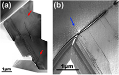
Figure 7. CS-TEM images of regions where the +c-wing of one growing crystal overlaps the adjacent crystal: (a) [1-100]GaN zone axis multibeam; the red arrows show a few TDs escaping from blocking process; (b) bright field scanning TEM (STEM) image; The blue arrow shows a TDs propagating from the bottom to the top crystal when they touch.
Download figure:
Standard image High-resolution image3.4. Third step: coalescence
The coalescence step results in the formation of new crystalline defects as observed in figure 8. This is a general observation in the case of heteroepitaxial 3D growth with high lattice mismatch. In fact, even in the case of very good epitaxial relationship between the deposited islands and the substrate, coalescence of independently grown islands always results in defect formation [24, 25]. The involved defect formation mechanism may be related to stress relaxation phenomena. 3D-grown crystals are most of the time elastically relaxed by lattice planes bending at the crystal facets. Therefore, at the coalescence, the lattices of connecting islands are out-of registry which is compensated by the formation of crystalline defects. A previously reported photoluminescence study demonstrates that uncoalesced islands are fully relaxed whereas continuous films are in compression on these samples [12]. This result reinforces the proposed hypothesis about defect formation.
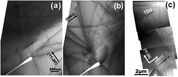
Figure 8. Bright field CS-TEM images of a coalescence boundary with  (a) and
  (b); (c) bright field STEM image of a coalescence boundary along the [1-100]GaN zone axis.
Download figure:
Standard image High-resolution imageMost of the defects created in the coalescence boundaries in our samples are perfect dislocations. Very few BSFs are detected. Diffraction contrast TEM allows analysing the nature of the dislocations. Figures 8(a) and (b) are bright field images using  and (0002) respectively. The observed dislocations are in-contrast using
  and out-of-contrast using
  which is characteristic of a-type dislocations. In fact, both a − and a + c-type (not shown here) dislocations have been observed at the coalescence boundaries.
The most commonly observed behaviour for the newly created TDs is the one shown in figure 8. First TDs lines lie in a (11-20) plane and they then bend in the (0001) plane and propagate to the surface (figure 8(c)). This may be understood by considering the evolution of the morphology during the coalescence step observed in figure 6. When the growth conditions change from step 2 to step 3, the coalescence first occurs between the (11-20) facet of the bottom crystal and the bottom facet of the top crystal (red circle in figure 6(a)). TDs are created in the coalescence boundary which is situated in the (11-20) plane. At this stage the growth front is formed by a (0001) facet from the top crystal and a (11-20) facet from the bottom crystal. The changes of the growth conditions induce a drastic increase of the (11-20) facet growth rate (larger distance between AlN interlayers along this direction after the change of growth conditions as seen in figure 6(b)). As a result, the (11-20) facets grow over the (0001) facets. The newly created dislocations bend in the c-plane following the growth front between these 2 facets. The rapidly growing (11-20) facets disappear to the benefit of the (11-22) facets which allows a flattening of the films. After flattening of the film, dislocation lines remain in their stable c-plane until emerging on the surface of the film (figure 8(c)). TDs should therefore be mainly observed in (0001) planes separated by the period of the pattern.
The best way to visualize the defect distribution and to quantitatively determine their densities at the surface of the films is to observe them in PV orientation. A reliable study requires the observation of a sufficiently large surface area. Figure 9, which is a multibeam image along the (22-43) zone axis, is formed by the juxtaposition of several TEM micrographs and is more than 20 μm large which represent more than 2 periods of the pattern. Three coalescence boundaries are included in this image (red arrows). The defect distribution is clearly highlighted: most of the defects are situated in coalescence boundaries, confirming previous cathodoluminescence (CL) observations [12] and TEM CS observations. The observed defects are either perfect dislocations or BSFs. In a thin TEM sample, emerging dislocations appear as dots. On the other hand, BSFs situated in inclined c-plane have the characteristic fringe contrast of inclined planar defects. In fact the dislocations observed in figure 9 are similar to the ones emerging at the surface in figure 8(c).
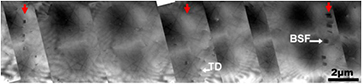
Figure 9. PV-TEM image along the [22-43] zone axis. Examples of TDs and BSFs contrasts are highlighted.
Download figure:
Standard image High-resolution imageSeveral images like that one have been acquired for a total surface area of 574 μm2. The number of counted dislocations and BSFs are 389 and 19, respectively. The average width of BSFs is 210 nm. The dislocation density is 7 × 107 cm−2. The BSFs density has been determined by measuring their total length and dividing it by the surface area. The BSFs density is 70 cm−1. These measured densities are coherent with CL measurements on larger zones and obtained on different areas distributed on the surface of several 2 inch semipolar templates [12].
4. Discussion and conclusion
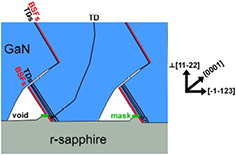
The microstructure of 3S-PSS GaN films contains crystalline defects which may be divided in two categories. The first category concerns the defects nucleated within growth islands. These defects are BSFs present in the NL, TDs resulting from the growth on sapphire c-facets and BSFs created in the −c-wings. The mastering of the GaN polar growth allows one to control the propagation direction of TDs. Playing with the growth parameters, a controlled 3D-growth is obtained. The gradual islands morphology changing from truncated to perfect pyramidal cross-section shape imposes on TDs to bend in the c-plane. Most of the defects (TDs and BSFs) emerge on islands top facets in stripe-like regions of small width except the few TDs which escape the bending process. The width of the defective stripe-like regions is directly related to the width of the sapphire c-facet and to the extension of the −c-wing. From this controlled microstructure, playing again with the growth conditions, it is possible to bury these defective areas preventing the propagation to the coalesced surface of most of the defects of this first category.
The second defect category results from the coalescence of growth crystals. We assume that the formation of these defects result from elastic relaxation of the lattice mismatch at the facets of the islands. This mechanism seems to be intrinsic to 3D heteroepitaxial-growth in systems with large lattice mismatch and it may be difficult to avoid these defect formations. The global microstructure of 3S-PSS films including the different growth steps already shown in figures 4–8 is schematically represented in figure 10. The two categories of defects are shown.
Figure 10. Schematic representation of the behaviour of defects in 3 S-PSS; TDs are in black and BSFs in red. The mask, the void and the orientation of GaN are indicated.
Download figure:
Standard image High-resolution image
With the patterns and successive growth parameters that we have used (11-22), semipolar GaN films on 2 inch sapphire substrates with TDs density of 7 × 107 cm−2 and extremely low BSFs density of 70 cm−1 are reproducibly obtained. The TDs density can be favourably compared to the best values for polar GaN films heteroepitaxially grown on c-sapphire [26]. The TDs density is similar and the BSFs density lower than the best published results for heteroepitaxially grown (11-22) GaN layers [27, 28].
From the understanding of the microstructure of 3S-PSS GaN films, it is possible to propose at least two ways to decrease further the defect density. The first one is to use a pattern with a longer period reducing the number of coalescence boundaries. But, in this case, a thicker layer has to be grown in order to obtain a flat continuous film. Another possibility should be to grow thick layers by halide vapour phase epitaxy (HVPE). The TDs density could be reduced when the films thickness increases as observed in the case of polar growth. The involved process is related to TDs lines reorientation facilitating their interaction and annihilation [29]. The limitation of this approach in semipolar GaN films is related to the presence of BSFs which remain in the c-plane without the possibility of interactions therefore propagating to the surface whatever the thickness of the films. The BSFs density being already extremely low, this limitation should not be a problem when using 3S-PSS films as template for HVPE-regrowth.
Acknowledgments
The authors want to thank the French network METSA for giving us the opportunity to access to the TITAN 80–300 microscope and to T Neisus (University P. Cézanne, Marseille) for his expert help in the use of this microscope. E Beraudo (CRHEA) is also acknowledged for his assistance in the realization of the figures. M Leroux (CRHEA) and G Feuillet (CEA-LETI) are also acknowledged for a critical reading of the manuscript.
One of us (FT) acknowledges the support of Saint-Gobain- Lumilog and the financial support (Grant no 2012–15783) from the region Provence-Alpes-Côtes d'Azur (PACA).