

Abstract
Mn2Au is one of the few candidate materials for antiferromagnetic spintronics requiring ordered metals with a high Néel-temperature and strong spin–orbit coupling. We report the preparation of epitaxial Mn2Au thin films by rf-sputtering. Structural characterization by x-ray and electron diffraction demonstrates a high degree of atomic order and the temperature dependence of the resistivity is typical for a good metal. The magnetic properties of the samples are studied by the investigation of Mn2Au/Fe bilayers. Exchange bias effects are observed, which present strong evidence for antiferromagnetic order in the Mn2Au thin films. Small domains of  500 nm are visualized in the exchange coupled Fe thin film.
Export citation and abstract BibTeX RIS
I. Introduction
The usual concepts of spintronics rely on the magnetization of ferromagnets (FMs) for data storage and manipulation. An alternative concept is based on the use of antiferromagnets (AFMs), e.g. by employing the direction of the staggered magnetization for data storage. An indirect read-out of this direction is possible by coupling the AFM to a FM creating an exchange spring, but also direct approaches based on magnetotransport effects exist: for instance an anisotropic magnetoresistance (AMR) effect was observed in the AFMs Sr2IrO4 [1] and FeRh [2]. With Cu point contacts on Sr2IrO4 even large magnetoresistance effects up to 28% could be obtained [3]. A prominent example is the large tunneling anisotropic magnetoresistance effect (TAMR  160%) between the AFM IrMn on one side and non-magnetic Pt on the other side of an MgO barrier [4]. For such devices, ordered metallic AFM compounds combining high Néel temperature and large spin–orbit coupling effects are required [5]. However, only few compounds with such properties exist. Examples are CuMnAs [6] and Mn2Au [7, 8]. One benefit of antiferromagnets for spintronics is the potentially ultrafast spin-dynamics, which in AFMs is typically 2–3 orders of magnitude faster than in FMs [9]. Another advantage of AFMs is their insensitivity in external fields due to their zero net magnetization. However, this property also poses a major challenge in antiferromagnet-based spintronics: New approaches for the controlled manipulation of the AFM spin-orientation have to be identified and investigated. For ordered AFMs with strong spin–orbit interaction it was recently suggested to use short current pulses for the manipulation of the spin-axis direction. Considering the tetragonal AFM compound Mn2Au, based on Néel-order spin–orbit torques fields current densities of 108–109
  were estimated to reorient the spin-axis within the easy ab-plane [10]. Such high current densities are of the same order of magnitude as required for spin–orbit torque switching of e.g. Ta/CoFeB structures and can only be applied as short pulses (
 10–100 ns) to narrow conductor channels (
 1–10 nm) using thin films (
 1–10 nm) [11, 12]. Band structure calculations [13] predict strong anisotropies (up to 50%) of the density of states of Mn2Au for the different alignments of the staggered moment, i.e. either parallel to the easy (1 1 0) or to the hard (0 0 1) axis of the tetragonal compound. This anisotropy significantly exceeds the corresponding anisotropy of IrMn (about 10%), thus a larger TAMR is expected for Mn2Au.
Experimentally it was confirmed that Mn2Au indeed is a simple antiferromagnet with the magnetic moments on the Mn sites aligned in the ab-plane and a Néel temperature well above 1000 K [8]. It was also demonstrated that (1 0 1)-oriented Mn2Au thin films can be grown by MBE, showing exchange bias effects with Fe layers [7]. However, for the predicted current switching of the AFM domains, the current has to be applied within the ab-plane requiring (0 0 1)-oriented thin films, whose growth and characterization is described here.
II. Preparation and characterization
Within the preparation and analysis cluster described in [14] epitaxial Mn2Au thin films in (0 0 1)-orientation were prepared by rf-sputtering from a single stoichiometric target on Al2O3(1  0 2) substrates with Ta(0 0 1) buffer layer. The growth rates amounted to
  0.1 nm s−1, typically a buffer layer thickness of 18 nm was used for growing Mn2Au thin films of typically 62 nm thickness.
Figure 1 shows the results of a x-ray diffraction (XRD)  -scan of a Al2O3(1
  0 2)/Ta(1 0 0)/Mn2Au(0 0 1) sample indicating negligible impurity phases and a small portion of misaligned Mn2Au(1 0 1). The inset shows a rocking curve (ω-scan) of the Mn2Au (0 0 2) peak indicating a mosaicity of
  . The Mn2Au phase formation was observed for substrate temperatures
  during deposition between 500 °C and 650 °C. However, the most narrow XRD rocking curve was obtained with
  °C. Figure 2 shows an XRD φ-scan of off-specular (1 0 1) and equivalent peaks of Mn2Au(0 0 1) and (1 1 0) and equivalent peaks of Ta(1 0 0) demonstrating the in-plane order and epitaxial relation of the Mn2Au thin film and buffer layer. The scans show that the ab-plane of Mn2Au(0 0 1) has the same orientation as the ab-plane of the Ta buffer layer, as expected due to the small lattice mismatch of only 0.6%. The surface order of the Mn2Au(0 0 1) thin films is demonstrated by the electron diffraction image (RHEED) shown in figure 3. The arrangement of the sharp RHEED spots on semi-circles is characteristic for scattering from a 2-dimensional, i.e. smooth surface with structural in-plane order.
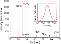
Figure 1. XRD  -scan of a Al2O3(1
  0 2)/Ta(1 0 0), 18 nm/Mn2Au(0 0 1), 62 nm thin film demonstrating the orientation of the Mn2Au-(0 0 1)-axis perpendicular to the substrate. The inset shows the rocking curve (ω-scan) of the Mn2Au-(0 0 2) peak.
Download figure:
Standard image High-resolution image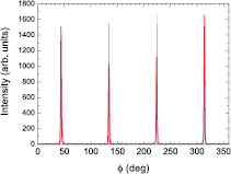
Figure 2. XRD φ-scans of off-specular Mn2Au-(1 0 1) (red) and Ta-(1 1 0) (blue) peaks showing the in-plane order and epitaxial relation of a Al2O3(1  0 2)/Ta(1 0 0), 18 nm/Mn2Au(0 0 1), 62 nm thin film.
Download figure:
Standard image High-resolution image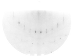
Figure 3. Inverted electron diffraction (RHEED) image of a Al2O3(1  0 2)/Ta(1 0 0), 18 nm/Mn2Au(0 0 1), 62 nm thin film. The sharpness of the spots and their arrangement on semi-circles (Ewald-sphere) indicates a well ordered smooth surface.
Download figure:
Standard image High-resolution imageTemperature dependent measurements of the resistivity R(T) of a lithographically patterned Al2O3(1  0 2)/Ta(1 0 0), 18 nm/Mn2Au(0 0 1), 62 nm/AlOx, 2 nm thin film revealed metallic behavior of the Mn2Au layer with a residual resistivity ratio of RRR
  3 (figure 4). The room temperature resistivity amounts to
 cm, which is similar to the specific resistivity of the Ta buffer layer and a typical value for a good metal. The small specific resistivity of the Mn2Au thin films is beneficial considering the required current densities and associated heating effects for the predicted current induced switching of AFM domains [10].

Figure 4. Temperature dependent resistivity of a Mn2Au(0 0 1) thin film. The Al2O3(1  0 2)/Ta(1 0 0), 18 nm/Mn2Au(0 0 1), 62 nm/AlOx, 2 nm sample was lithographically patterned into a stripe of 100 μm width. The specific resistivity of the Mn2Au thin film was obtained by subtraction of the conductivity of a reference Al2O3(1
  0 2)/Ta(1 0 0), 18 nm/AlOx, 2 nm sample, which has a similar specific resistivity as the Mn2Au(0 0 1) layer.
Download figure:
Standard image High-resolution imageIII. Magnetic domain structure
To test the antiferromagnetic nature of the Mn2Au(0 0 1) thin films, a 5 nm thick epitaxial Fe(001) layer (with a 5 nm Al protective capping layer) was deposited in situ on top of the Mn2Au. This bilayer should act as an exchange coupled system, if cooled in a high enough magnetic field through the blocking temperature. This method was e.g. successfully used to image antiferromagnetic CoO domains at an Fe/CoO interface [15]. Considering the expected high Néel temperature of Mn2Au [7], we used a relatively thin film (7 nm), attempting to reduce the ordering temperature. We cooled the sample from 375 K in a field of 1 T parallel to the Fe(1 0 0), i.e. Mn2Au(1 1 0) axis. In figure 5 we show the results of temperature dependent measurements of the magneto-optical Kerr-effect (MOKE) from 300 K down to 10 K. There are two remarkable features of these hysteresis measurements: first, there is a negligible exchange shift. The slight shift observed is not reproducible upon temperature cycling, which could indicate some training effect. Second, the coercivity of the Mn2Au/Fe heterostructure at 300 K is much larger (15 mT) than for a bare Fe film (1 mT) and increases dramatically with decreasing temperature. The coercivity almost doubles between 300 K and 10 K with the biggest change between 300 K and 175 K. This strongly suggests the presence of an exchange anisotropy acting on the Fe film, which, however, is randomly oriented in the film plane. Obviously the field cooling protocol had little effect on the alignment of the AF domains in the field direction. This, in turn, implies that the cooling field was still applied below the blocking temperature of the Mn2Au film. However, Wu et al previously followed a similar protocol and were able to demonstrate an exchange bias effect in Fe/Mn2Au(1 0 1) [7]. This could be related to the different growth direction of their Mn2Au thin films or to a different morphology, which may result in uncompensated magnetic moments at the interface. For our Mn2Au(0 0 1) thin films magnetometry using a superconducting quantum interference device (SQUID) gave no indication for any uncompensated moment.
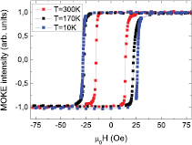
Figure 5. MOKE hysteresis measurements of a Al2O3(1  0 2)/Ta(1 0 0), 18 nm/Mn2Au(0 0 1), 7 nm/Fe, 5 nm/AlOx,5 nm sample at different temperatures.
Download figure:
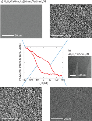
Standard image High-resolution imageFigure 6(a) shows Kerr microscopy images obtained from a Mn2Au(60 nm)/Fe(5 nm)/Al(5 nm) sample at different field values in the film plane and at 300 K. The hysteresis shown in the center is obtained by integrating the MOKE intensity over the entire image. Close to coercitivity the domain structure is grainy indicating an Fe domain size of typically 500 nm. This is by far smaller than the domain size of a Fe film on a bare substrate, as shown in figure 6(b). Furthermore, the domains do not show a preferred orientation. Thus the domain structure visible here confirms the notion already gained from MOKE hysteresis measurements that the Fe domains are associated with an exchange coupling to the Mn2Au layer. This coupling causes an imprint of the AFM domains onto the Fe domains, allowing for a visualization of the antiferromagnetic domain structure. It turns out that the antiferromagnetic domain structure is random in space, which explains the missing exchange bias.
Figure 6. (a) MOKE-microscopy images of a Al2O3(1  0 2)/Ta(1 0 0), 18 nm/Mn2Au(0 0 1), 60 nm/Fe, 5 nm/AlOx, 5 nm thin film and corresponding hysteresis loop obtained integrating the MOKE intensity over the complete image. (b) MOKE-microscopy images of a Al2O3/Fe(5 nm)/Al(5 nm) thin film for comparison.
Download figure:
Standard image High-resolution image
In order to exclude that the observed domain structure is dominated by properties of the Fe instead of the Mn2Au, we repeated the investigations using Permalloy instead of Fe as a ferromagnetic layer. The obtained domain structure is identical to the Fe case, providing additional evidence for a dominating contribution of the exchange coupling with the Mn2Au thin film to the ferromagnetic domain formation.
IV. Summary
Epitaxial Mn2Au thin films with (0 0 1)-orientation were grown by rf-sputtering at optimized substrate temperatures on Al2O3 (1 02) substrates with Ta(1 0 0) buffer layers. The thin films show very good metallic properties and a high degree of crystallographic ordering within the film as well as on the surface. Evidence for antiferromagnetic order forming small domains in Mn2Au was provided via magnetic characterization of ferromagnetic thin films exchange coupled to Mn2Au. Thus rf-sputter deposition of antiferromagnetic Mn2Au thin films of high epitaxial quality in the required orientation for future spintronics applications was demonstrated.
Acknowledgments
This work is supported by the Graduate School of Excellence Materials Science in Mainz (MAINZ, GSC 266) and the DFG.