
Abstract
III–V nanowires (NWs) have been envisioned as nanoscale materials for next-generation technology with good functionality, superior performance, high integration ability and low cost, because of their special growth modes and unique 1D structure. In this review, we summarize the main challenges and important progress of the fabrication and applications of III–V NWs. We start with the III–V NW growth, that significantly influences the NW morphology and crystal quality. Attention is then given to the fabrication of some advanced III–V structures composed of axial and radial junctions. After that, we review the advantages, challenges, and major breakthroughs of using III–V NWs as solar energy harvesters and light emitters. Finally, we attempt to give a perspective look on the future development trends and the remaining challenges in the research field of III–V NWs.
Export citation and abstract BibTeX RIS

Content from this work may be used under the terms of the Creative Commons Attribution 3.0 licence. Any further distribution of this work must maintain attribution to the author(s) and the title of the work, journal citation and DOI.
1. Introduction
Recently, the nanowire (NW) with a one-dimensional (1D) columnar shape has gained great attention [1–3]. The diameter of the NW is normally from several nanometres to hundreds of nanometres, while its length can go to several tens of micrometres. Semiconductor NWs only confine carriers in 2 dimensions, and hence allow them to propagate freely along the third dimension. If the diameter of the NW is sufficiently small, carriers are subjected to quantum confinement [4, 5]. Because of the good optoelctronics properties of III–V semiconductor materials, a wide range of methods have been used to fabricate III–V NWs, such as laser ablation, metal-organic vapour phase epitaxy, chemical beam epitaxy, and molecular beam epitaxy [6–10]. In addition, III–V NWs can also be synthesized through solution phase. However, it is difficult to control the NW crystal structure and growth orientation by using solution phase [11].
In the NW geometry, III–V materials can exhibit different features compared with their thin film counterparts. Due to the small footprint, III–V NWs have very good strain tolerance, which can accommodate large lattice and thermal expansion coefficient mismatch between the III–V nanowires and substrates [12, 13]. It can also solve the antiphase domain problem when polar III–V NWs are grown on non-polar substrates [14, 15]. Therefore, III–V NW can facilitate the integration of high-quality materials on a wide range of substrates. During their growth, most III–V NWs can adopt both the zinc blend (ZB) and the wurtzite (WZ) crystal structure by changing the growth conditions. This is very difficult to achieve by the traditional thin film technology [16]. The change in crystal structure can significantly change the band structure, and hence the optical and electrical properties of the materials [17, 18]. As a result, the NW can offer additional freedom for band structure engineering. Moreover, with the unique shape, it can lead to novel subwavelength optical phenomena, such as polarization anisotropy and optical birefringence [19, 20]. Therefore, the NW can serve as a platform to understand the fundamental properties of materials, which could lead to new discoveries and applications.
Benefited from the properties of the NW geometry, NW devices can potentially exhibit superior performance compared with their thin film counterparts. For photovoltaic devices, the NW geometry will enhance light–matter interactions, that can significantly enlarge its absorption cross section [21]. In addition to the good antireflection and the superior light trapping formed by NW forests [22–24], the NW devices can have a significantly enhanced light absorption [25–28]. The NW structure also provides an efficient charge separation and carrier collection with marginal recombination loss [29]. Therefore, it is possible to fabricate high-efficiency photovoltaic devices with a smaller amount of deposited material compared with the thin film devices. It has been demonstrated that the NW solar cells (SCs) can even break the Shockley–Queisser limit, due to its enhanced absorption cross section [21]. In addition, the NW has a very large surface-to-volume ratio, which can provide a large surface area and thereby lower the barrier for chemical reaction [30, 31]. This is beneficial for chemical energy conversion, such as water splitting devices. On the other hand, the emitters could have the superior light extraction efficiency by incorporating NW structures [32]. Therefore, the NW emitters could potentially have high efficiency and lower energy consumption. The NWs can also act as the gain material, waveguide and the resonance chamber at the same time [33, 34]. With the extremely small size, the NW is highly favourable as compact light sources that are suitable for device miniaturization. It can be widely used in the integrated nanophotonic and optoelectronic systems, such as high-resolution microdisplays, ultrahigh density optical information storage, and multiplexed chemical/biological analysis.
Although NW devices with promising properties have been recently demonstrated, the NW growth and the NW device fabrication are still very challenging. Due to the small dimension, unique geometry and the special growth modes, the NW growth is much more sensitive to the substrate condition and the growth parameters compared with its thin film counterpart. In most cases, the growth window for NWs is very narrow and the NW growth directions, crystal phase, composition and junction are difficult to control. Moreover, for the NW device, the design theories and the fabrication processes are quite different from the traditional thin film device. During these years, with the great effort of researchers, more and more new phenomena have been discovered and a lot of new theories have been brought out. In this review, we will summarize the important novel discoveries and theories on III–V NW fabrication and their application in optoelectronics. Special attention will be given to the key factors, which can influence the III–V NW morphology, crystal quality, junction formation and the device performance. Some of the topics may have been discussed in previous reviews [35–37]. However, due to the fast development of the NW research, we are aming to give readers an updated and more exhaustive overview about these areas.
2. III–V NW fabrication
The droplet catalysed growth is the most used method in the NW fabrication. In this section, we will summarize the NW morphology and crystal structure adjustment based on, but not limited to, this growth mode. Special attention will be paid to the influence of the substrates and the growth conditions.
2.1. Fabrication methods
NWs can be fabricated through the top-down and bottom-up methods. The top-down method is to etch a mask covered bulk material to form NWs [38]. Lithographic techniques and dry etching are commonly used [39]. This method has limitations in making small NWs, especially for the ones with diameter smaller than 10 nm. Furthermore, the top-down method will lose the NW advantages for integrating materials with large lattice and thermal mismatch, because it needs to grow bulk material before the NW fabrication. But due to the lack of staking faults and the high-quality NW/substrate interface, it has gained great attention [40]. Dhindsa et al achieved highly ordered vertical gallium arsenide NW arrays by this method (figure 1(a)) [39]. On the other hand, the bottom-up method can fabricate NW in the angstrom level and offer better ability to handle strain [1]. This method is to grow 1D NWs from the substrates by suppressing the 2D growth. It can be divided into two categories: catalyst-free growth and catalytic growth. The catalyst-free growth mode is a vapour–solid (VS) growth. In most cases, this growth mode needs a mask. The NWs grow out of the mask openings and form a columnar shape. It relies entirely on the anisotropic growth by stabilizing certain crystal facets and enhancing the growth in only 1D through the growth condition control. This growth method is known as selective area growth (SAE). The SAE mode can achieve very high NW uniformity and very good NW morphology (figure 1(b)) [41]. In some special cases, the catalyst-free NWs can also be grown without any mask, such as the self-induced GaN NWs [42]. The catalyst-free growth mode has the advantages of achieving axial junctions with good sharpness compared with the droplet-catalysed growth mode, because it is free from the reservoir effect that can delay the composition change due to the solubility of materials in the droplet [43–45]. In contrast, the catalytic growth needs a nanoparticle catalyst to assist the NW growth [46]. The mask pattern can also be used in this growth mode, which functions as a position controller (figure 1(c)). Therefore, researchers prefer to call it position controlled growth [47]. This mode can be further divided into foreign metal catalysed and self-catalysed growth [48]. Au is the most used foreign catalyst, while group-III elements are normally used as the self-catalyst for III–V NW growth. Both Au-catalysed and self-catalysed NWs are grown via the droplet-catalysed vapour–liquid–solid (VLS) growth mode [10, 49]. In 1960s, Au was used as the catalytic droplet to grow Si nanowhiskers [50]. Later on, the Au catalyst was used for III–V NW growth [51]. But concerning the contamination probability of Au in the III–V NW, the self-catalysed growth mode was then developed. The droplet catalyst is widely believed to act both as a source material collector and the reaction catalyst. However, its catalytic role is still under debate [52]. During growth, the droplet collects the source materials. Once it is oversaturated, the NW growth starts by the material precipitation. The droplet size determines the NW diameter, if the NW sidewall is free from radial growth. So far, the Au- and self-catalysed growth modes are the two commonly used growth methods for III–V NWs.
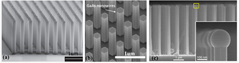
Figure 1. (a) Scanning-electron-microscope (SEM) image of top-down etched GaAs NWs. Adapted with permission from [39]. Copyright 2014, IOP Publishing Ltd. (b) SEM image of SAE-grown GaAs NWs. Reprinted with permission from [41] Copyright 2014, American Chemical Society. (c) VLS-grown GaAs NWs. Inset is the tip of the NW. Adapted with permission from [46]. Copyright 2014, American Chemical Society.
Download figure:
Standard image High-resolution imageAu has a moderate melting temperature, and hence is able to form low-melting alloys [48]. Most group-III and V elements have high diffusion coefficients in it [48]. Therefore, it is quite suitable to be the catalyst for NW growth. Moreover, Au has good resistance to oxidation and other parasitic reactions, which can simplify the growth preparation [48]. During growth, the Au is not a fast consumption material and hence less sensitive to the changes of parameters, compared with the group-III material in the self-catalytic droplet. The growth window for the Au catalysed growth, such as the growth temperature and V/III ratio, is much wider compared to other growth modes. This offers much greater freedom in controlling the NW fabrication, such as axial/radial selectivity, crystal phase, growth direction, and growth rate. For example, Joyce et al developed a two-temperature Au-catalysed growth technique by using a high-temperature 'nucleation' step and a prolonged low-temperature 'growth' step [53]. The temperature difference between the two steps was larger than 100 °C. With this large temperature adjustment, they achieved high vertical-yield and pure-phase ZB GaAs NWs. Furthermore, due to the large growth window, it can facilitate the growth of III–III–V type of NWs with large composition coverage, such as the  (
( ),
),  (
( ) and
) and  (
( ) [54–57]. The Au-catalysed growth technique can also facilitate the heterostructural fabrication with large group-III composition switch, such as axial GaSb/InAs(Sb) NW heterostructures [58]. Despite all those advantages, Au is unpopular in some research areas. It is well known that Au is a forbidden element in CMOS processing, since it can form mid-gap energy states in Si and hence degrade the device performance [59, 60]. Most importantly, Au has high solid diffusivity, which is easy to cause contamination to the exposed fabrication equipment, and is extremely hard to remove. Therefore, the NW catalysed by Au metal is incompatible with the Si-based IC industry. For the NW itself, it has been shown that Au can be incorporated into the GaAs and InAs with a doping level in the order of 1017–1018 cm−3 [60, 61]. But it is still under debate whether the Au would degrade the performance of NW devices [62]. For example, a direct comparison, between Au- and self-catalysed GaAs NWs, shows that the Au-catalysed NW has much lower photoluminescence intensity and shorter carrier lifetime [59]. However, some other researchers have shown that the Au catalyst has no significant influence on the NW properties, especially for the optical properties [63, 64]. Furthermore, the non-disappearance of the Au can seriously affect the NW shell growth. The Au can sustain the VLS axial growth during the side facets VS shell growth (figure 2(a)) [65]. The different growth modes can lead to different growth rates, composition profiles, and doping concentrations [66]. The removal of Au droplets for shell growth requires taking the sample out of the growth chamber [67], which could cause extra cost and contamination.
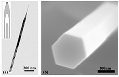
Figure 2. (a) Transmission electron microscope (TEM) image of a gold-catalysed GaP/GaAsP core–shell NW. Inset is the illustration of the growth mechanism of the NW shells. Adapted with permission from [65]. Copyright 2009, IOP Publishing Ltd. (b) SEM image of a self-catalysed GaAsP core–shell NW.
Download figure:
Standard image High-resolution imageThe group-III metals have a low melting point and high boiling temperature, and hence are highly suitable for making the catalyst droplet. In the self-catalysed growth, the catalyst material is the same as the group-III element in the NW. Therefore, it does not cause any contamination from the catalyst droplet, unlike for the foreign metal catalysed growth. Moreover, the group-III droplet has a lower surface energy compared with that of the Au droplet, which is favourable for ZB crystal phase formation [68, 69]. After the NW growth, the catalytic droplet can be consumed by crystalizing it into the NW by only opening the group-V source. This can terminate the droplet-catalysed axial growth. As a result, the radial VS shell growth can be separated from the axial VLS growth. Figure 2(b) shows a SEM image of a self-catalysed GaAsP core–shell NW. However, due to the consumable feature of the droplet, it is necessary to keep the dynamic balance between consumption and accumulation of group-III species by carefully tuning the growth parameters, especially the growth temperature and V/III ratio. Therefore, the self-catalysed growth has limitations in terms of growth conditions, which makes it difficult to adjust the NW crystal structure. In addition, it can also cause trouble for growing the III–III–V type of NWs. Different group-III elements have quite different temperature features, especially the diffusion length. But a vast majority of the group-III atoms in the NWs are diffused from the substrate and the NW sidewalls during the NW growth [70]. Therefore, there will be large differences in the optimal growth conditions between each species, especially the growth temperature [71, 72]. As a result, the self-catalysed growth has a narrow growth window, and hence is difficult to provide an optimal condition for more than one group-III elements at the same time. Paek et al reported that the In composition in the Ga-catalysed InGaAs NW growth is only 1–2% in spite of a high In/Ga ratio [72]. Heiss et al also demonstrated that the In composition in the group-III assisted InGaAs NW growth is limited to 3–5%, despite the change of the growth temperature [73].
2.2. Influence of the substrate and its preparation
III–V semiconductor materials have quite a lot of interesting and useful optoelctronic properties, such as the direct band-gap, high absorption coefficient, high carrier mobility and large solar spectrum coverage [74]. The hybridization, between III–V and non-III–V materials, can achieve advanced complementation [75–77]. For example, the research on the integration of III–V materials on the more mature and cost-effective silicon platform has been pursued for more than 40 years [78–81]. This integration is believed to be able to create novel optoelectronic devices, such as high-performance silicon-based III–V lasers and high-efficiency but cost-effective SCs [82–87]. However, in the traditional thin film growth, the material combination and the substrate choice are still limited by strain caused by the mismatches of lattice and thermal expansion coefficient [81, 88]. In addition, the antiphase domain is another big problem for growing the polar III–V material on a non-polar monoatomic substrate, such as Si and Ge [15]. All those long-standing issues can be solved by using the NW structure. This is benefited from the small cross section of the NW structure and hence the small contact area with the substrate, which can provide very efficient lateral strain relaxation. For example, the epitaxial growth of InAs NWs on Si with a lattice mismatch of up to 11.6% has been demonstrated [89, 90]. It has been predicted that when the NW diameter is smaller than a certain value, depending on the mismatch level, the NW/substrate interface can be defect free [12, 13]. Yoshimura et al demonstrated that an InGaAs NW with a diameter of 90 nm can be grown without defects on GaAs (1 1 1)B despite a lattice mismatch of 2.1% [91]. For NWs with larger diameter than a critical value, the strain will relax through the formation of misfit dislocations [14, 92]. The misfit dislocations have been observed at the InAs/Si interface with a period of ~2.9 nm and GaAs/Si of ~8.0 nm [90, 93]. However, there is still no consensus on the exact critical diameter for each lattice mismatch. Normally, no threading dislocation can be found at the upper part of the NWs in most cases even if the diameter is larger than the critical diameter, which is probably due to the layer-by-layer NW growth mode [14] or the bending of the threading dislocations to the sidewalls [94]. Therefore, the dislocation can be constrained at the NW/substrate interface to prevent them from degrading the performance of NW devices. As a result, by using the NW structure, it can facilitate the integration between different material systems and pave the way to the use of inexpensive substrates. It has been demonstrated that, besides the single crystalline and polycrystalline substrates, the NWs can also be grown on graphene, carbon nanotube, fibre-textured silicon thin film and amorphous Si [95–101]. The III–V NWs can even be grown on glass and the indium tin oxide [102, 103].
The substrate surface conditions play a critical role to achieve the 1D NW growth. For the Au-catalysed growth, it is quite common to grow on oxide-free substrates. Especially for the NW growth on Si substrates, the presence of native oxide can be detrimental [104, 105]. Therefore, the preparation for silicon substrates needs to be very carefully carried out to avoid oxidation at ambient environment [12]. In contrast, the oxide-free substrate is unfavourable for the catalyst-free (except nitride NWs) and self-catalysed growth. The large nucleation area can hinder the anisotropic growth and the group-III metal droplet formation. In order to suppress the 2D planar growth and immobilize the catalyst droplets [106], it is necessary to use a mask for III–V NW growth, such as SiOx or SiNx. On the mask, there are nanometre-sized holes, through which the substrate lattice can be exposed to the source flux, as shown in figure 3(a). During the growth, the material deposition on the mask is energetically unfavourable. Therefore, the adatoms on the mask will diffuse around and in the end desorb back to the vapour or participate in the NW growth at the holes, as shown in figure 3(b). The mask can generally be divided into two categories. One type of mask has well-defined position and size of holes by the pre-defined patterns. Here, we call it 'patterned mask'. The other is the mask with self-assembled random pinholes, such as thin native oxide on Si substrates. Here, we define this type of mask as 'pinhole mask'.
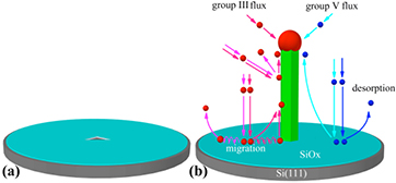
Figure 3. (a) Illustration of the mask-covered substrate with a nano-sized hole. (b) Illustration of the VLS growth mode of NWs on mask-covered substrate. Adapted with permission from [9]. Copyright 2013, American Chemical Society.
Download figure:
Standard image High-resolution imageThe patterned mask is usually made by nanoimprint or electron-beam lithography (EBL) on SiOx or SiNx covered substrates [47, 107]. The mask layer thickness is usually between 10 and 40 nm [67, 108]. By using the patterned mask, the NW density and position can be well controlled, which is highly favourable for achieving a good NW uniformity, designing NW photonic crystals and fabricating devices. Furthermore, the insulating mask layer can be helpful for suppressing the device current leakage. For the patterned growth, the cleanness of the patterned hole is very critical for achieving a high yield. Especially for the patterned Si substrate, the fast-regrown oxide in the holes can significantly affect the yield [109]. Even if the pattern is loaded into the growth chamber right after being cleaned by a HF solution, the Si oxidization still cannot be completely avoided and hence leads to poor uniformity, low yield and bad repeatability, as shown in figure 4(a). A high temperature deoxidization step before the NW growth is a very effective method to clean the pattern. For the growth on patterned III–V substrates, it is comparatively easy to do the pattern cleaning due to the low desorption temperature of the III–V native oxide. But for the patterned Si substrate, a higher temperature (>850 °C) is needed due to the high desorption temperature of the Si oxide [109]. For the Au-catalysed growth, if the high temperature cleaning is conducted with the Au droplet in the patterned holes, the Au droplet preferentially moves to the edges of the hole [110]. In addition, the Au droplet can react with the underlying substrate, which can cause the formation of an Au-based alloy and even hide the alloy droplet underneath the pattern mask. As a result, the patterned growth can be suppressed [110]. Boulanger et al introduced a high-temperature Ga pre-filling step to bring the Au droplet back to the centre of the patterned holes and achieved a yield exceeding 99% [110]. After the high-temperature cleaning, the patterned hole is clean and fully open. Therefore, the available nucleation area in the hole is large and the group-III atom consumption rate is very fast. For the self-catalysed VLS mode, the NW growth can be suppressed, because the group-III droplet formation is difficult in the holes. As a result, only VS growth is available to form catalyst-free grown NWs or clusters (figure 4(b)). In order to assist the group-III catalytic droplet formation in the clean patterned holes, a group-III pre-deposition step to assist the catalyst droplet formation is needed before introducing the group-V source for the NW growth. The self-catalysed GaAsP NW has been achieved repeatedly on patterned Si substrates by combining the high-temperature cleaning and the Ga pre-deposition method (figure 4(c)). This solved the low-repeatability issue for the patterned NW growth on Si substrates [111]. Except for the yield, the patterned mask can also strongly affect the NW morphology. If the size of patterned hole is bigger than the catalyst droplet size, the patterned hole is only partially covered by the catalyst droplet and there is still some vacant area available for VS nucleation in the hole. This can cause the parasitic VS growth at the base of the NW, and hence severely degrade the NW morphology (figure 4(d)). Therefore, the patterned hole size should not be bigger than the catalyst droplet size. For catalyst-free growth mode, the patterned hole size is not so critical if the growth is on a polar substrate. However, if the growth is on non-polar substrates, such as Si, a small patterned hole size is more favourable because the small opening can reduce the number of 2D islands in the initial nucleation process [14, 112].
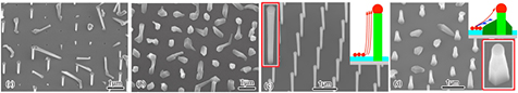
Figure 4. SEM images of self-catalysed GaAsP NW growth on patterned substrate (a) without high-temperature cleaning; (b) with high-temperature cleaning, but without Ga pre-deposition; (c) and (d) with both high-temperature cleaning and Ga pre-deposition. The hole sizes for (c) and (d) are ~50 nm and ~135 nm, respectively [109].
Download figure:
Standard image High-resolution imageThe pinhole mask is used more frequently in the self-catalysed NW growth [9], and sometimes in catalyst-free NW growth [113]. It is usually formed by using a SiOx layer with a thickness of a few nanometres. The SiOx layer can be a thermal oxide layer, organic chemicals converted oxide layer, several monolayers of oxidized Si, and even the native oxide layer of the Si substrate [114–119]. When the SiOx layer is thin enough, there will be some pinholes that penetrate through the oxide layer to expose the substrate lattice [120–122]. During growth, the group-III adatoms can accumulate at the pinholes to form catalyst droplets [116, 120]. The NW can then grow epitaxially with the substrate out of the pinholes. The increase of the NW density is associated with the increase of the pinhole density, which can be controlled by the reduction of the oxide layer thickness [116]. But if the oxide thickness is too thin or even oxide free, it will lead to the 2D epitaxial growth such as clusters or thin film, rather than NW growth [122, 123]. It is also suggested that the increase of NW density can be achieved by increasing the mask surface roughness [114, 123]. The rough surface can reduce adatom diffusion length and create more catalyst droplets. In addition, by increasing the roughness, it can increase the number of the pinholes, which punch through the mask layer and reach the substrate lattice. On the other hand, the pinholes could be created by the reaction between the catalyst droplet and the mask layer, which can etch through the mask [124]. Therefore, the suppression of NW growth on a too thick oxide mask could be due to the difficulty to etch through.
Because the NW is epitaxially connected with the substrate, the substrate crystalline orientation has significant influence on the growth azimuth of the NW relative to the substrate. III–V NWs are commonly observed growing vertically on III–V (1 1 1)B substrates (figure 5(a)). For some other commonly used substrate crystalline orientations, the NWs tend to grow inclined with an angle relative to the substrate (elevation angle), due to the non-vertical 〈1 1 1〉B directions. For example, the NWs on the (0 0 1) substrate prefer growing along the two 〈1 1 1〉B directions with an elevation angle of ~35°, as shown in figure 5(b) [124, 125]. Except the energetically favoured 〈1 1 1〉B orientations, it is also possible to grow the NW along the other directions, such as the 〈1 1 1〉A, 〈1 1 0〉 and 〈1 0 0〉 [126–129]. Choosing the substrate orientation is a straightforward method to force the NW growing along those directions [130, 131]. But the substrate pretreatment is critical. For example, Krishnamachari et al demonstrated that Au-catalysed InP NW can be grown vertically on InP (1 0 0) substrates, see figures 5(c) and (d) [130]. But if an initial high temperature annealing before the NW growth was used, the NWs tend to grow along the 〈1 1 1〉B orientation. This could be due to the appearance of the (1 1 1)B facets created by the Au etching of the substrate during the annealing. The similar phenomenon was also found in the growth of 〈1 1 1〉A GaAs NWs on the GaAs (1 1 1)A substrates [126]. In addition, the liquid–vapour interface energy can also be used to govern the NW growth direction. Wang et al demonstrated that the NW growth direction can be switched reversibly between 〈1 1 1〉B and 〈1 0 0〉 by controlling the droplet liquid–vapour interface energy via changing the In content in the Au droplet (figures 5(e) and (f)) [132]. By increasing the In filling time from 0 to 15 s, they increased the 〈1 0 0〉 growth yield on InP (1 0 0) substrates from 27 ± 1% to 97 ± 1%.
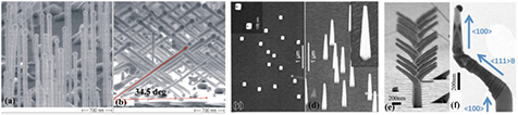
Figure 5. SEM images of self-catalysed GaAs NW growth on (a) GaAs(1 1 1)B and (b) GaAs(0 0 1) substrates. Reprinted with permission from [124]. Copyright 2008, AIP Publishing LLC. (c) SEM top view and (d) tilted view (30°) of InP wires on InP(0 0 1). Reprinted with permission from [130]. Copyright 2004 AIP Publishing LLC. InP NWs grown on InP (1 0 0) substrate with growth direction changing (e) from 〈1 0 0〉 to 〈1 1 1〉 and (f) from 〈1 0 0〉 to 〈1 1 1〉 and back to 〈1 0 0〉. Reprinted with permission from [132]. Copyright 2013 American Chemical Society.
Download figure:
Standard image High-resolution imageWhen grown on a non-polar substrate, such as Si and Ge, the 〈1 1 1〉A direction can be used as the equivalent 〈1 1 1〉B direction [133]. For example, on the Si (1 1 1) substrate, in accompanying the vertical growth, the NWs can also grow along three extra inclined directions (figure 6(a)) [89, 134]. The multi-azimuth growth of NW can lead to some advantages, such as enhancing the light scattering. However, it can also cause trouble for the device fabrication. Therefore, suppressing the NW growth along non-vertical directions is of importance in some cases. Covering with a III–V buffer layer is a direct way to endow the non-polar substrate with the polar feature. Ghalamestani et al achieved the 100%-yield well-aligned InAs NW growth across the full wafer by covering a 2 inch Si (1 1 1) wafers with a thin InAs epitaxial layer (figure 6(b)) [135]. Similar results have been demonstrated in the InP and GaAs NW growth on Si substrates [136–139]. Moreover, the substrate surface termination and reconstruction could also determine the NW growth direction [90]. For example, the As-incorporated Si3+ and In-terminated Si1+ surface structures could have the (1 1 1)B feature [90]. Tomioka et al demonstrated the growth of the catalyst-free InAs NW with a vertical yield of 95% on patterned Si (1 1 1) substrates by forming the As-terminated Si3+ reconstruction at low temperature (400 °C) (figure 6(c)) [90]. Besides the polarity, the strain at the substrate/NW interface is also suggested to have significant influences on the NW growth direction [12]. This strain can be relieved by introducing twin planes during the initial NW nucleation step. As a result, the nucleus can change to another 〈1 1 1〉 directions, along which the NW grows. In some cases, multiple twins can generate before NW growth along the final 〈1 1 1〉 direction. Therefore, the NW axis is not always exactly parallel to one of the substrate 〈1 1 1〉 directions. For example, GaP/Si (0.4%) and GaAs/Ge (0.1%) tend to grow vertically, while InP/Ge (3.7 %) and GaAs/Si (4.1%) do not show the preference to any of the four equivalent 〈1 1 1〉 directions, and InP/Si (8.1%) and InAs/Si (11.6%) favour the non-vertical direction [12, 104]. Therefore, according to this strain model, using a thin film buffer is likely to achieve vertical NW growth onto the non-polar substrates with a large mismatch. For example, it can use a short GaP segment to separate the GaAs NW from directly contact with the Si substrate. In addition, Chuang et al proposed that smaller catalyst droplets were beneficial for growing well-aligned NWs, which could also be due to the reduction of the strain at the NW/substrate interface [140]. In additional to the strain, Russo-Averchi et al suggested that changing the relative size between the GaAs seed and the Ga droplet could also control the twin defect formation, and hence the NW growth direction [141].
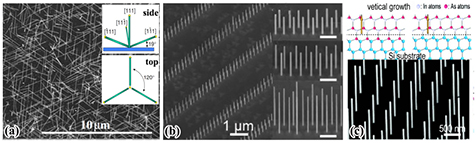
Figure 6. (a) Top view SEM images of InAs NWs grown on Si(1 1 1). Insets are the illustrations of the NW growth direction [89]. (b) Uniform and position-controlled InAs NWs on InAs-covered Si (1 1 1). Insets show the higher magnification images of NWs with different diameters. Adapted with permission from [135]. Copyright 2012, IOP Publishing Ltd. (c) Illustrations of vertical NW growth with As-incorporated Si3+ surface (top left) and In-terminated Si1+ surface (top right). SEM image of vertical InAs NW array grown on As-terminated Si3+(1 1 1) by SAG (bottom). Adapted with permission from [90]. Copyright 2008 American Chemical Society.
Download figure:
Standard image High-resolution image2.3. Stacking faults and crystal structure control
Normally, in thin film growth, the nitrides show hexagonal WZ structure while other III–V materials exhibit a cubic ZB phase. But for NW growth, they can be adjusted to adopt both ZB and WZ crystal structures, which is difficult to achieve in thin film growth. The WZ and ZB phases have different band structures. For example, it has been demonstrated that the indirect band gap ZB material, such as GaP, can have direct band gap when changed to the WZ phase [16]. The change of band structure can lead to different photonic and electric properties [142]. For example, the optical polarization can be changed from being parallel to the NW axis to being perpendicular to it if the crystal structure is switched from ZB to WZ [17, 18], which could be used for polarization sensitive photodectectors [142, 143]. In most cases, the WZ/ZB phase junction has type II band alignment [144–147]. This band discontinuity can be used to fabricate phase QD and lead to charge confinement [148]. In addition, the NWs, constructed by stacking WZ and ZB, can separately confine the electrons and holes to reduce their wave functions overlap, which can cause a rapid quench of the direct-band-gap photoluminescence (PL) emission but keep the long-lifetime indirect-band-gap PL emission and electrical conductivity [149, 150]. The carrier separation could provide a way to increase the lifetime of the hot carriers, which could be beneficial for photovoltaics. However, for electronic applications, stacking faults can act as scattering centres for carriers, and hence degrade the device performance [149, 151–155]. For example, increasing the defect density can decrease the carrier mobility of GaAs NWs from 2250 ± 70 to 1200 cm2 V−1 s−1 [156]. Even a single twin plane is believed to be able to change the symmetry and the strain of the crystal, which could modify the carrier effective mass and hence the carrier mobility [157, 158]. Moreover, Wallentin et al reported that the ZB segments in WZ InP NWs can act as traps for electrons [159]. For undoped InP NWs, the trapped electron concentration can be as high as 4.6 × 1018 cm−3, which led to low conductivities and mobilities. Therefore, the ability to selectively tune the crystal structure is of great importance for not only offering additional freedom for band structure engineering but also improving the device performance.
The intermixing of ZB and WZ structures happens when the NW is grown in the 〈1 1 1〉 crystal direction of the cubic cell or the 〈0 0 0 1〉 direction of the hexagonal cell. The difference between WZ and ZB crystal structures arises from the difference in the third nearest-neighbour atom spacing, which is shorter for WZ structure, causing an energy difference smaller than 25 meV per ortho pair [160–162]. The physical origin of the different phases is the competition between the Coulomb force and the steric hindrance [163]. The Coulomb force is decided by the iconicity of the material and tends to reduce the bond length of the atoms, while the steric hindrance is linked with the atom size and try to increase the bond length [163, 164]. The material with high iconicity and small steric hindrance prefers WZ structure. This could be one of the main reasons why the III-nitride NWs tend to adopt WZ structure, and the III-antimonide favours ZB, while the other III–V NWs with moderate iconicity and steric hindrance values are easy to have mixed stacking faults. Avit et al demonstrated WZ GaN NW growth with a defect-free length of tens of micrometres (see figures 7(a)–(c)) [165]. Conesa-Boj et al showed that GaAsSb NWs can have pure ZB crystal phase down to the first bilayer (figure 7(d)) [107]. Yang et al reported that InSb NWs are able to keep the ZB crystal phase even when the diameter is as small as 4.5 nm (figure 7(e)) [166]. By increasing the Sb composition, the phase pure WZ InAs NW can change to single phase ZB InAsSb NW, and there is a transition regime between these two extremes with intermediate stacking faults (figures 7(f)–(l)) [155, 167]. So far, the detailed nucleation process is still unclear and there is no theory to explain the exact reasons why the NW crystal structure can be adjusted between the two phases.
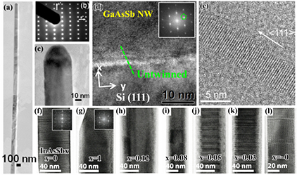
Figure 7. TEM images of GaN NWs: (a) low-magnification image on a long GaN NW; (b) Electron diffraction pattern from (a); (c) High-resolution TEM (HRTEM) image showing the top of (a). (a), (b) and (c) are adapted with permission from [165]. Copyright 2014 American Chemical Society. (d) HRTEM image of the GaAsSb NW/Si substrate interface [107]. (e) HRTEM image of the InSb NW. Adapted with permission from [166]. Copyright 2010 American Chemical Society. (f)–(l) TEM images of InAsSb NWs with different Sb composition. (f) pure WZ; (g) pure ZB; (h) pure ZB; (i) ZB with occasional twin planes; (j) ZB with pseudo-periodic twin planes; (k) mixed ZB and WZ with frequent stacking faults and twins; (l) Sb content below X-ray energy-dispersive spectroscopy (XEDS) detection limits, WZ structure with regular stacking faults [167].
Download figure:
Standard image High-resolution imageControlling the growth direction is an effective way to change the crystal phase. Since the stacking faults happen in the 〈1 1 1〉B or 〈0 0 0 1〉 direction, avoiding this growth direction is a straightforward way to suppress them. It has been demonstrated that III–V NWs grown along the 〈1 0 0〉, 〈1 1 0〉 and 〈1 1 1〉A directions could be pure ZB and free from stacking faults [126–130, 168–170]. Among those directions, the substrate with 〈1 0 0〉 facet can accommodate the standard semiconductor process, which is highly desirable.
For the NWs inevitably growing along the 〈1 1 1〉B or 〈0 0 0 1〉 directions, it is suggested that the NW diameter plays a crucial role in controlling the crystal structure of the NWs. For example, Caroff et al presented that InAs NWs can be adjusted from almost stacking-fault-free WZ to pure ZB by increasing the diameter from 24 to 110 nm, as shown in figure 8 [171]. According to the thermodynamics, the decrease of the NW diameter can increase the surface-to-volume ratio and hence the free energy of each atomic pair [172]. In addition, the NW with WZ structure is beneficial for reducing the free energy due to the lower surface energy of the sidewalls compared with that of the ZB NWs [161]. Therefore, there is a critical radius under which WZ wires should be more stable than ZB wires [161, 173]. As reported by Shtrikman et al, thin GaAs and InAs wires on the order of 10 nm are found to be WZ and free of stacking faults [174]. However, the critical radius, predicted by considering the thermodynamic stability, is far too small (e.g. 12–32 nm) [161]. By changing the growth condition, the WZ phase can appear in NWs with a much larger diameter (>50 nm), while the ZB NW can be grown with a diameter as small as 5 nm [68]. Therefore, in addition to the thermodynamics, the nucleation kinetics should be considered as well in controlling the crystal structure of the NWs [175, 176].
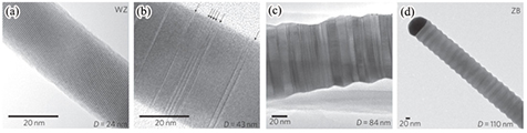
Figure 8. TEM images showing the diameter dependence of the crystal structure for an InAs NW from WZ to ZB. Adapted by permission from Macmillan Publishers Ltd: Nature Nanotechnology [171], copyright 2008.
Download figure:
Standard image High-resolution imageAlthough the nature behind the droplet catalysed growth is still under debate [177], it has been suggested that the nucleation occurs preferentially at the perimeter of the NW-metal particle interface, called triple phase line (TPL), where the vapour, liquid and solid phase meet. At the TPL, a high droplet supersaturation will promote the wurtzite nucleation [176, 178]. Therefore, the droplet supersaturation can be used to control the NW crystal structure. Johansson et al found that the supersaturation of the droplets can be significantly affected by the diameter-dependent Gibbs–Thomson effect [179]. They also noticed that the Gibbs–Thomson effect is still significant even at a relative large diameter. By taking the Gibbs–Thomson effect into consideration, they predicted much larger and more realistic critical radii for ZB/WZ phase transition (>50 nm) compared with that given by only considering the thermodynamics (see figures 9(a)–(c)). Moreover, the growth condition can also significantly affect the droplet supersaturation. It has been proposed that the droplet supersaturation can be decreased with the reactant concentrations inside [180, 181]. As demonstrated by Johansson et al, the percentage of WZ structure in the GaP NW is significantly decreased by reducing the Ga concentration and hence the supersaturation of the Au droplet (figures 9(d) and (e)) [182]. In addition, the supersaturation can also increase with decreasing the growth temperature [180, 181]. As demonstrated in InAs NWs, the proportion of WZ in the NW increases significantly with decreasing temperature [171, 179]. By periodically adjusting the growth temperature, Caroff et al achieved the axial WZ/ZB InAs NW superlattice (figure 9(f)) [171]. Although the supersaturation can be used to control the crystal phase effectively, it alone is still not enough to explain some extreme cases. For example, although the droplet supersaturation is very high at a very fast growth rate, it still tends to produce ZB NWs [183, 184].
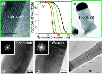
Figure 9. (a) WZ structure fraction as a function of InAs NW diameter as estimated by nucleation calculations (solid curves) and observed in experiments (data points). (b) TEM image of a pure WZ InAs NW with a diameter of 17 nm. (c) TEM image of a pure ZB InAs NW with a diameter of 133 nm. (a)–(c) are reprinted with permission from [179]. Copyright 2010 American Chemical Society. (d) and (e) are TEM images of GaP NWs grown with low (pulsed Ga flux) and high (continuous Ga flux) Ga concentration Au droplets, respectively. Adapted with permission from [182]. Copyright 2009 American Chemical Society. (f) TEM image of WZ–ZB superlattice InAs NW grown by temperature adjustment. Reprinted by permission from Macmillan Publishers Ltd: Nature Publishing Group Nanotechnology [171], copyright 2009.
Download figure:
Standard image High-resolution imageThe surface energies at the vapour–liquid interface have been found to be able to significantly affect the NW nucleation and its crystal structure. The droplet with a low surface energy can suppress the nucleation at the TPL [68]. When the nucleation is away from the TPL, the occurrence of ZB phase is preferred [178]. In the Au-catalysed growth, the increase of the group-III element concentration in the Au droplets can reduce the surface energy, because group-III metal has lower surface energies than pure Au [185]. Dheeraj et al demonstrated the switch in GaAs NWs from WZ to ZB structure by changing the droplets from Au-rich to Ga-rich and the reversible crystal structure switch (figures 10(a)–(d)) [69]. Gil et al showed that when the Ga concentration is higher than 0.62 in the Au droplets, GaAs NWs with pure ZB can be achieved even if the diameter of the NW is as small as 5 nm (figure 10(e)) [68]. Soda et al demonstrated the change of the crystal structure from WZ rich to mixed WZ/ZB polytype by increasing the Ga content from 25–50% to 75% in the Au droplet [186]. Apart from the group-III element, Lehmann et al suggested that the group-V element could also lower the liquid–vapour surface energy of the droplet to suppress the WZ nucleation [187]. By increasing the group-V flux to about 50 − 150 times, the Au-catalysed GaP, GaAs, InP, and InAs NWs can quickly switch from WZ to ZB (figures 10(f)–(j)). Moreover, Joyce et al demonstrated that GaAs NWs can have completely defect-free ZB structure (figures 10(k)–(m)) by increasing both Ga and As fluxes [183]. Besides the group-III and V elements, some other elements, such as Zn and S dopant, are also able to change the surface energy and the barrier for the WZ nucleation. It has been shown that the Zn can change the InP crystal structure from WZ to ZB, while the S doping induces WZ structure [188–192]. Moreover, Joyce et al also suggested that the surface energy of the external vapour–nucleus facet, in combination with its orientation, can determine the probability of twin formation [193]. Under the high group-V coverage conditions, the vapour–nucleus facet reconstructions can make the ZB nucleation more energetically favourable. The InAs NW, for a wide range of NW diameters (~30–100 nm), can be adjusted to pure ZB (pure WZ) by using low (high) temperature and high (low) V/III ratio (figures 10(n)–(q)).

Figure 10. (a) TEM image of a WZ/ZB/WZ GaAs NW axial phase junction. (b), (c) and (d) are electron diffraction patterns obtained from each segment in (a). (a)–(d) are adopted from [69]. (e) HRTEM images of a pure ZB GaAs NW with a radius of 5−6 nm. Reprinted with permission from [68]. Copyright 2014 American Chemical Society. (f) Illustration of the group V precursor change during the preparation of WZ/ZB III–V NW heterostructures. (g)–(j) are the TEM images of single WZ/ZB phase junctions with different III–V materials. The measurement was using the WZ-related 0 0 0  double diffraction spot for imaging. The scale bars are 200 nm. (f)–(j) are adapted with permission from [187]. Copyright 2013 American Chemical Society. (k) Twin density versus group III flow for GaAs NWs with different constant V/III ratios. (l) and (m) are the TEM images of NWs with slow and high growth rates, respectively. The former one has twin defects; while the latter is twin-free. (k)–(m) are adapted with permission from [183]. Copyright 2009 American Chemical Society. (n) and (p) are the TEM images of pure ZB and WZ InAs NWs grown at group V rich and deficient conditions, respectively. (o) and (q) are the electron diffraction patterns from (n) and (p), respectively. (n)–(q) are adapted with permission from [193]. Copyright 2010 American Chemical Society.
Download figure:
Standard image High-resolution imageThe shape of the catalyst droplet also has important influence on the crystal structure of the nucleation. As proposed by Krogstrup et al, when the droplet has a low wetting angle and moderate size, a large proportion of its TPL will be in direct contact with the edge of the NW top facets and promote the WZ formation (figure 11(a) middle) [194]. If the droplet size reduces or increases, the TPL will recede from the edge back to the top (figure 11(a) left) or proceed to the side facets (figure 11(a) right), respectively. Both of those two cases will suppress the TPL nucleation and ZB phase is favourable. Rieger et al investigated the Ga droplet consumption process of the GaAs NWs [195], and found that when the droplet contact angle was reduced from about 137° to 90°, the crystal structure was changed from ZB to WZ. When the droplet was further consumed, the contact angle kept at 90°, but the TPL receded to the NW top facet and the crystal structure was changed back to ZB. By changing the droplet size, they demonstrated the reversible switch of the GaAs NWs between WZ and ZB crystal structure. Similar results are also reported by Munshi et al [196]. Additionally, Yu et al suggested that the shift of the TPL along the sidewall can cause the defects formation (figure 11(b)) [197], which is supported by their observation of the appearance of a defect-section between the ZB and WZ segments during their Ga droplet consumption (figure 11(c)). Furthermore, the growths of ZB/defect-section superlattices and WZ/defect-section superlattices by changing the Ga droplet size were achieved (figures 11(d) and (e)). Apart from the droplet shape related TPL position change, Algra et al proposed that the droplet distortion can lead to the twin plane formation [188]. According to their model, during the ZB InP NW growth, the tilted angles of the side facets can cause the droplet deformation (figure 11(f)). During the growth, the droplet deformation becomes more and more intense. When the deformation energy is large enough, it will introduce the twin plane to release the strain and change the side facet tilt directions to start a new strain accumulation process. In addition, the periodical balance between the strain energy accumulation and release can lead to the formation of the twinning superlattice (figure 11(g)). Beside from the above factors, the variation of the growth conditions could be a cause for the introduction of stacking faults in the NWs [198]. Most of those previously mentioned parameters are highly coupled. For example, the change of the flux can change the droplet composition. The composition is connected with the droplet surface energy. The variation of the surface energy can lead to the deformation of seed particles, and as a result, it can affect the droplet contact angle [189]. Moreover, the growth temperature can affect the adatom surface diffusion and desorption, the solubility and the chemical content of the seed particle, the effective V/III ratio, and the droplet chemical potential. Therefore, all the factors need to be taken into consideration for the design, growth and characterization of NW structures.
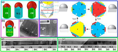
Figure 11. (a) Illustration of the relationship between the TPL position, the nucleation location and the nucleation crystal structure. (b) Illustration of the defect formation by TPL shift along the sidewall. (c) HRTEM image of the GaAs crystal structure transition during Ga droplet consumption by As flux. (d) and (e) are the TEM images of the ZB/defect-section and WZ/defect-section superlattices, respectively. (c)–(e) are adapted with permission from [197]. Copyright 2012 American Chemical Society. (f) Illustrations of relationship between sidewall tilt, the NW cross section shape change, the droplet distortion and the twining defect formation. (g) TEM image of the InP NW twinning superlattice. Inset is the overview of the twinning superlattice [188]. (f) and (g) are adapted with permission from Macmillan Publishers Ltd: Nature, copyright 2008.
Download figure:
Standard image High-resolution image3. III–V NW junctions
The NW axial and radial junctions are highly important for the design of advanced NW devices, and hence their applications. The special growth modes and the nanoscale prismatic shape can provide both advantages and challenges for NW junction growth. In this section, we will summarize the phenomenons during NW junction formation and discuss the key factors.
3.1. Axial junction
For the integration of lattice-mismatched materials, the formation of misfit dislocation is inevitable if the thickness of thin film exceeds a critical thickness [199]. In contrast, the NWs have a small cross section, which can efficiently relax the strain [200]. In addition, the axial junction can distribute the strain across the interface, which can further relax the strain gradually and elastically. It has been demonstrated that the strain of the heterojunction InAs/InP (figures 12(a) and (b)) and InAs/InSb (figures 12(c) and (d)) can be effectively relaxed elastically within a few nanometres across the junction [200, 201]. Therefore, for an axial NW heterojunction strcuture with lattice mismatch, there will be a critical diameter below which there is no interface dislocation introduced regardless of the length [202, 203]. The dislocation-free heterojunctions have been realized, such as the GaAs/GaP and InAs/InP [200, 204]. However, if the strain is large, the heterojunction could introduce misfit defects, such as the defects reported in GaAs/GaSb and InAs/InSb heterojunctions [205]. For the applications, the axial junctions can offer more freedom in the band structure engineering and need new theories for the device structure design. For example, quantum dots (QDs) can be grown within the NW by stacking the material axially [206]. This is different from the traditional Stranski–Krastanow QDs, which needs the strain to form the dot [207–211].

Figure 12. (a)  and (b)
  strain profiles across a InAs/InP heterojunction. Insets show the
  and
and  strain map of the InAs/InP NW interface [200]. (c)
  and (d)
  strain profiles across a InAs/InSb heterojunction. Insets show the
  and
and  strain map of the InAs/InSb NW interface [201].
Download figure:
Standard image High-resolution imageThe axial NW junctions have been achieved with the combination of various materials, such as GaAs/GaAsP, InAs/InSb, GaAs/GaAsSb and InSb/GaAs [212–215]. The integrations can even be done between different material systems, such as GaAs/Ge, GaP/Si, and GaN/ZnO [216–218]. For self-catalysed growth, the growth of III–III–V materials is more difficult than that of III–V–V materials. As mentioned in the section of growth modes, different group-III elements have quite different optimized growth conditions. But the growth window of the self-catalysed NWs is small, leading to the difficulty to provide the optimum growth condition for more than one group-III elements at the same time. Changing the growth conditions could be a solution to grow the III– III–V materials, but the consumable feature of the catalyst for the self-catalysed NWs makes it difficult to be realized. In contrast, the group-V elements have very high vapour pressure and very short diffusion length. They participate in the NW growth by directly impinging on the catalyst droplet from the vapour phase [219], which makes them less sensitive to the growth temperature compared with the group-III elements. Therefore, the self-catalysed heterojunction could be achieved by keeping the group-III element and changing the group-V elements, such as the GaAs/GaAsSb heterojunction [215]. On the other hand, the Au-catalysed growth mode has a large growth window due to the unconsumable feature of the Au catalyst droplet. Therefore, compared with the self-catalysed growth mode, it has more freedom in the axial junction growth. For example, the GaSb/InAs and InP/GaAs heterojunctions have been realized with high-quality hetero-interface [58, 190, 220, 221].
Keeping the axial junction straight is critical for the NW device fabrication. However, the straightness of the axial junction with a pair of materials is usually nonreversible, especially for the pair with the different group-III elements. For example, the NW is normally straight for the growth of GaAs on InAs, while the growth of InAs on GaAs is commonly observed to be kinked (figures 13(a) and (b)) [222]. This kink is explained in terms of the relevant surface/interface energy [223]. The surface/interface energy is increased when InAs epilayer is grown on GaAs. To minimize the surface/interface energy in the material system the InAs material adopt island growth [222]. The continued island growth will lead to kinking [224]. There exists a critical value of the increase in the surface/interface energy, below which the heterojunction can still keep straight. Krogstrup et al found that the junction can keep straight with a threshold Ga value ~40–50%, while the fraction of the kinked wires increased rapidly for Ga with higher percentage (figures 13(c) and (d)) [225]. The change of group-V elements in the heterojunction has the same surface/interface energy limitation, but the effect is much smaller, due to the small change in the surface/interface energy [52]. The summary of the surface/interface energy change for different material combinations can be found in [52]. A gradual composition change across the heterojunction interface could be an effective way to achieve straight growth. The introduction of a buffer layer can also solve the kinking issue. Hillerich et al showed that adding a Ge interlayer can successfully grow Si directly onto the GaAs NW (figure 13(e)) [216]. Hocevar et al also demonstrated that GaAs NW segments could be inserted between the Si NW segments by using GaP buffer layers (figure 13(f)) [217]. However, those solutions can affect the heterojunction quality, such as the sharpness. In contrast, the control of NW crystal structure can avoid kinking and keep the interface sharp [226]. Messing et al demonstrated by changing the InAs crystal structure from ZB to WZ, that InAs can successfully be grown on top of GaAs NWs with a sharp interface (figures 13(g)–(j)) [226].
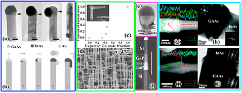
Figure 13. (a) TEM images and (b) illustrations of the kinking development at the initial growth of InAs on GaAs NWs. Adapted with permission from [222]. Copyright 2007. John Wiley & Sons. (c) plot of the fraction of kinked wires as a function of a GaAs mole fraction. (d) SEM image of the InAs/ /InAs axial heterojunctions with 47% GaAs content in the GaLnAs segment. (c)–(d) are adapted with permission from [225]. Copyright 2009 American Chemical Society. (e) TEM image of the Si/Ge/GaAs heterojunctions. Adapted with permission from [216]. Copyright 2013 American Chemical Society. (f) TEM image of the Si/GaP/GaAs/GaP/Si NW heterojunctions [217]. Reprinted by permission from Macmillan Publishers Ltd: Nature Communications, copyright 2012. (g) High-angle annular dark field TEM (HAADF-TEM) image with corresponding XEDS line scans across and along the NW, showing the interfaces of the ZB GaAs/WZ InAs heterostructure. (h) Conventional TEM image of the same NW with electron diffraction pattern reveal the crystal of each segments. Growth direction is from left to right. (i) Same measurement as (g) but showing the interfaces of the WZ GaAs /WZ InAs heterostructure. (j) Same measurement as (h) but on NW shown in (i). Growth direction is from left to right. (g)–(j) are reprinted with permission from [226]. Copyright 2011 American Chemical Society.
Download figure:
Standard image High-resolution imageThe sharpness of the axial junction is another important factor on the band structure design, such as the formation of axial quantum dots and superlattices. However, for the droplet-catalysed growth, the atomic sharp group-III heterojunction is difficult to obtain, due to a reservoir effect caused by the large solubility of group-III elements in the droplet [42–44]. For example, Heiß et al reported that their  /GaAs heterostructures need a transition time in the order of 1000 s to reach the maximum concentration of indium in their
  alloy [227]. Moreover, it has been found that the solubilities of different group-III elements are directly connected in the Au droplet. For example, during the InAs NW growth, the introduction of Ga flux can reduce the equilibrium composition of In in the Au droplet, and vice versa [44]. In addition, different elements have different thermodynamic affinities towards the Au nanoparticle. For example, the thermodynamic affinity of In is greater than that of Ga in the Au nanoparticle. Therefore, it is easier to expunge the Ga by increasing the In concentration in the droplet, while expunging the In out of the droplet by increasing the Ga concentration is more difficult [228]. This could cause the different abruptness of different element switch sequences (figures 14(a)–(c)) [225]. As reported by Paladugu et al, the interface (atomically sharp) between InAs and GaAs is sharper than the interface (~50–70 nm) between between GaAs and InAs [190, 224, 225]. In contrast, the group-V elements have low solubility in the droplet and it depletes quickly in the droplet after turning off the source flux. Therefore, with the group-V element switch, it is easy to achieve sharp composition transition in the axial NW heterojunctions. For example, Jabeen et al fabricated axial GaP/GaAsP NW superlattice and the transition width between segments was ~1 nm, corresponding to roughly 3 interfacial monolayers [212]. The atomically sharp and dislocation-free interfaces have also been demonstrated in the InAs/InP NW heterojunctions (figures 14(d) and (e)) [200, 229, 230].

Figure 14. (a)–(c) are scanning TEM (STEM) and EDX data of InAs/ /InAs double heterojunctions. Reprinted with permission from [225]. Copyright 2009 American Chemical Society. (d) HAADF-STEM overview image of an InP/InAs heterojunction NW with the bright areas showing the InAs segments [200]. (e) A high-resolution HAADF-STEM image shows the atomically sharp interface, free from dislocations, between the InAs and the InP segments [200].
Download figure:
Standard image High-resolution image3.2. Radial junction
Due to the 1D columnar shape and small footprint size of the NW, the shell of NWs has much better strain tolerance compared with their thin film counterparts. It has been found that the NW core can share part of the mismatch strain, which can drastically reduce the strain in the shell [231–234]. For example, Skold et al found that by adjusting the GaInP shell composition and thickness, the strain can shift the GaAs core energy band gap by up to 240 meV (figure 15(a)) [235]. Montazeri et al also reported that a 50 nm diameter GaAs core can shift the free exciton emission energy by 260 meV when covered by a 25 nm thick GaP shell (figure 15(b)) [236]. It was predicted that for a given lattice mismatch, there is a critical core radius, below which the coherent shell growth can have no limit on the thickness [237, 238]. Furthermore, for a given core radius, there is a critical shell thickness, below which no defects will form [237, 238]. In general, this critical shell thickness is much larger than that of the thin film counterpart. As demonstrated by Nazarenko et al, the GaAs/In0.2Ga0.8As core/shell heterojunction with 2% lattice mismatch can have a defect-free shell thickness of 160 nm which is much thicker than the 10 nm of its thin film counterpart [239]. The plastic strain relaxation in the core–shell structure is through the formation of the line and loop edge dislocations for radial and axial directions, respectively (figures 15(c)–(i)) [240]. Normally, the strain relaxation is larger in radial directions than the axial direction [241]. As reported by Popovitz-Biro et al, the strain of the InAs/GaAs core–shell NW is partial and lager in the radial as compared to the axial direction, with the radial and axial misfits of 6 ± 1% and 4 ± 0.5%, respectively [240]. The strain can also be relieved through Stranski-Krastanov QD formation [242]. The InAs and InGaAs QD growth on the {1 1 2} surfaces has been demonstrated [243, 244]. The QD formation on the {1 1 0} facets are not energetically favourable. Instead, it tends to form big lumps [245, 246]. By covering the GaAs {1 1 0} facets with a thin layer of AlAs, the formation of InAs QDs can become available [207]. Due to the better relaxation of the lattice strain from the nanometre-sized curving side surfaces, the critical thickness for the QD formation on NWs is larger in comparison with that on the standard planar substrate [247–252].

Figure 15. (a) Band gap of the core and shell respectively as a function of the Ga content in the shell. Reprinted with permission from [235]. Copyright 2005 American Chemical Society. (b) PL spectra of GaAs/AlGaAs and GaAs/GaP NWs. Reprinted with permission from [236]. Copyright 2005 American Chemical Society. (c) Illustrations of the line dislocation plane. (d) HRTEM image of the coupled line dislocations from a cross-section of an InAs/GaAs core/shell NW shown in the inset. (e) and (f) are the lattice illustration of the coupled line dislocations shown in (d). (g) Illustration, (h) HRTEM image and (i) lattice illustration of the loop dislocation. (d)–(f) and (h)–(i) are adapted with permission from [240]. Copyright 2011 American Chemical Society.
Download figure:
Standard image High-resolution imageThe NW morphology can significantly influence the shell growth. If the core NW presents concavities, the shell deposition prefers to start at the convex edges of the concave regions, because it can effectively relax the strain and minimize the formation of misfit dislocations [249]. In addition, the concave region has lower chemical potential because of their surface curvature. This can drive the adatoms diffuse towards it, and hence make it grow faster. The formation of InAs nanorings has been demonstrated on GaAs NWs by this mechanism [249]. Moreover, due to the 1D shape, the growth rate can also be critical for the shell morphology. The slow growth rate was beneficial for achieving uniform shell thickness, due to the sufficient adatom diffusion [9]. At a too high growth rate, the material deposition at the tip of the NW was much faster, causing the defect formation. If the NW is not standing vertically on the substrate, the growth rate is even more important. Otherwise, it will lead to the irregular shell cross-section shape, making the NW shell much thicker at the front side facing the flux and much thinner at the back side [250]. The unequal shell thickness can cause the uneven strain distribution, and hence the bending of NWs [251, 252].
The different crystallographic planes of NW side facets also have significant influences on the NW radial growth. The self-catalysed and catalyst-free grown ZB NWs have {1 1 0} side facets [207, 253]. The WZ NW side facets, regardless of the growth modes, are either all {1 1  0} side facets, or all {1
  0 0} side facets [35]. The {1 1 0}, {1 1
  0} and {1
  0 0} faces are non-polar [35]. They normally produce an ideal prismatic shape with the side faces of equal length by uniform shell growth (figure 2(b)). The Au-catalysed ZB NW has {1 1 2} side facets, which are not all equivalent and can be subdivided into three {1 1 2}A and three {1 1 2}B faces. In each surface unit cell, the {1 1 2}A face has two three-fold coordinated group-III surface atoms and one two-fold coordinated group-V surface atom, while the {1 1 2}B face has two three-fold coordinated group-V surface atoms and one two-fold coordinated group-III surface atom [254]. Therefore, the group-III (group-V) atoms prefer attaching to the {1 1 2}A ({1 1 2}B) surface. Under high V/III growth condition, the {1 1 2}B facet grows slower and elongates as the {1 1 2}A surfaces grow out [255]. Therefore, the cross-section of the core–shell structure usually has a truncated triangular shape with elongated {1 1 2}B side facets and shorter {1 1 2}A side facets [255]. On the other hand, under low V/III growth condition, the {1 1 2}A facets tend to become more elongated [255]. The asymmetric shell growth can be used to selectively grow NW ribbons on the {1 1 2}A or B side facets [35, 256, 257]. In addition, the defects can also change the shell deposition morphology, because it can introduce some new nanofacets and hence change the local surface properties [255]. Kawaguchi et al demonstrated the QDs (quantum well) formation at the stacking-fault (stacking-fault-free) region of the WZ InP NW surface during the InAs shell growth [258].
For the ternary NW shell growth, the control of composition uniformity is more complicated compared to that of thin film growth, due to the non-planar surface of the NW and the different properties of elements. At the angled sidewall corners, the large effective curvature makes their surface chemical potential bigger than the adjacent side facets. This can drive the adatoms to diffuse from the corners to the adjacent facets, forming a capillary flux [259]. On the other hand, for the multicomponent material growth, the different elements have different cohesive energies (chemical bonding energies) with the substrate surface, which leads to different diffusion coefficients (diffusion lengths) [260, 261]. When growing a multicomponent shell, the corners are commonly observed to be rich in the elements with stronger bonding energies and shorter diffusion lengths, since the elements with lower bonding energies can diffuse more easily. It has been demonstrated that the growth of AlGaAs shells can cause an Al rich line along the corners of the shell (figures 16(a)–(c)) and it can even be pure Al for the AlInP shell [63, 259, 262–265]. These compositional inhomogeneities could change the local properties, such as band structure, doping efficiency and the strain, and hence affect carrier effective mass and transportation. The control of these effects can lead to new device geometries. For example, Heiss et al demonstrated that highly stable AlGaAs QDs can be formed in GaAs/AlGaAs core–shell NWs by phase segregation (figures 16(d)–(g)) [266]. As the axial QDs, the phase segregation QDs do not need the assistance of the strain. Moreover, their position relative to the NW centre can be controlled within nanometre range. Therefore, they can offer more advantages in band structure engineering and device structure design, compared with traditional Stranski–Krastanow QDs [267–270].
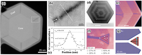
Figure 16. (a) STEM-HAADF image of a GaAs/Al0.3Ga0.7As core/shell NW cross-section with six dark Al rich stripes. (b) Detailed STEM-HAADF image of an Al-rich stripe as indicated by the dashed square in (a). (c) Al concentration profile obtained from an XEDS line scan perpendicular to the Al-rich stripe as indicated by the dashed line in (b). (a)–(c) are reprinted with permission from [264]. Copyright 2013 American Chemical Society. (d) STEM-HAADF image of a GaAs NW coated with multiple Al0.33Ga0.77As/GaAs shells. (e) Zoom-in STEM-HAADF image of (d). (f) Detail of the Al-poor quantum dot located within the fork-like Al-rich stripes. (g) Illustration of the quantum dot shown in (f) [266]. (d)–(f) are adapted by permission from Macmillan Publishers Ltd: Nature Materials, copyright 2013.
Download figure:
Standard image High-resolution image4. III–V NW optoelectronic devices
Due to the novel features of NWs, the III–V NW devices have the potential to bring breakthroughs in a wide range of fields, such as electronic, photonic, thermoelectric, photovoltaic, photoelectrochemical, mechanical, and biological areas [11]. Therefore, the NW has been considered as the next-generation technology with a potential for high performance and low cost. Especially, for the optoelectronic field, the NW has apparent superiority compared with the traditional thin film structures. In this section, we will focus on key breakthroughs and challenges of using NWs for the solar energy harvesters and the light emitters.
4.1. Solar energy harvesters
Energy conversion has become an increasingly important topic. Solar energy, which is plentiful, clean and renewable, is a strong candidate. The solar cells and photoelectrochemical cells are two major photovoltaic technologies to harvest the solar energy and have been investigated for decades in traditional thin film structures [31, 211, 271–276]. But so far, they are still hampered by the dilemma between the efficiency and cost. The lattice and thermal expansion coefficient mismatch between different material systems poses a strong restriction in the material combination and hence the device designs, which makes the devices either low efficiency or high cost. The NW structure, on the contrary, can produce high-quality material with low defect density [277, 278]. This makes the NW devices to be potential candidates for high internal quantum efficiency. Meanwhile, the ability of good strain relaxation between the NWs and substrates can facilitate the material combinations for covering the solar spectrum and create high-efficiency multi-junction devices. In addition, the NW can be grown on or transferred to the flexible and/or transparent substrates, which could enlarge the ubiquity of NW devices, such as integrating NW PV devices to buildings and fabric [279, 280].
The NW can also provide superior solar energy harvesting functions compared with thin film devices. Due to the special 1D structure with subwavelength diameter and high refractive index, the electromagnetic modes of the NW tend to be leaky and interact more effectively with the outside media [281]. This can enlarge the NW absorption cross section, which is much bigger than the physical size of NW [21]. In addition to the waveguiding modes which can guide light along the axis of the NW, the light absorption in the standing NWs can be more than one order of magnitude more efficient than that predicted from the Lambert–Beer law [21]. Furthermore, the leaky mode resonances can be easily tuned to a desired wavelength by changing the NW diameter, which can realize wavelength-selective absorption enhancement [39, 282–284]. In combination with the other NW geometry parameters, such as the NW length, profile and density, more freedom can be obtained in tailoring the absorption spectrum [282, 285–287]. This makes the current matching in multi-junction devices easier [282, 288]. When putting those individual NWs together to form NW arrays, they can provide a gradual transition in the refractive index [22]. Therefore, the light reflectance, caused by the abrupt difference in refractive index between two media, can be significantly reduced [22, 289–294]. Meanwhile, the NWs with subwavelength dimensions can provide strongly enhanced light scattering effect [23, 24]. This can significantly extend the light propagation path in the absorbing media and hence the effective optical thickness, making it well exceeding the Lambertian limit [25–28]. Garnett et al demonstrated that the light path length in their NW arrays can be enhanced by a factor of 73 compared with its actual physical thickness [295]. Both the efficient light antireflection and scattering offer the NW arrays with advanced light trapping ability in comparison with the thin film devices [24, 289, 292, 296, 297]. This can significantly enhance the broadband light absorption over a wide range of incident angles, especially the near and below band gap absorption [28]. Diedenhofen et al showed that the 3 μm-long InP NW/InP substrate can have an broad-band and omnidirectional absorbance of 97% in the visible and near-infrared wave range (400–850 nm) [287]. Zhang et al demonstrated that the 1.6 μm-long off-substrate GaAs NWs can have a solar-weighted above-bandgap absorptance of 94%, despite the low surface coverage of only 15% [284]. Due to the advanced light absorption, the NW device can use much smaller amount of deposited material but keep high absorption efficiency, compared with its thin film counterpart. This is beneficial for using less rare materials, and hence greatly reducing the cost. For example, ~1.5 μm-long InP NWs with only 12% surface coverage can generate a short-circuit current which is about 83% of the best InP planar cells [298]. Except the enhanced absorption, the NW can also guide the below band gap photons into the substrate. Diedenhofen et al found that more than 90% of the photons, with the energy lower than the InP absorption, were coupled into the underlying substrate by the InP NWs [287], which is highly favourable for multi-junction devices.
Due to their 1D core–shell structure, the NWs are also superior in extracting the generated carriers compared to the thin film structures. The collection efficiency of generated carriers depends strongly on the minority carrier diffusion length, which decreases with the increase of defect density [29]. The generated carriers will be wasted if they are more than one diffusion length away from the space charge region. On the other hand, in the traditional thin film device, the collection path of the generated carriers is parallel to the solar photon travelling path [299, 300]. Therefore, the requirement for a thick enough absorption material puts high demand on the crystal quality, so that the carriers can pass through without substantial recombination. In the case of the NW, light absorption and carrier extraction are de-coupled for the core–shell p–n junction device. It absorbs the light along the whole NW, while the generated carriers can be efficiently separated in the radial direction. The radial distance that carriers need to travel is normally much smaller than, or comparable with, the minority carrier diffusion length. Therefore, the orthogonally decoupled light absorption and carrier separation paths can lead to low bulk recombination, and hence high efficiency. In addition, the NWs have large surface-to-volume ratio, which offers large junction area, that can further enhance the charge separation efficiency. All those advantages enable us to use lower-purity and less-expensive materials with low minority carrier diffusion lengths. As a result, the use of NW structure can significantly reduce the device cost. These merits from NWs make the development of high-efficiency and low-cost SCs promising, and hence have the potential to bring revolutions to the solar energy harvesting technology.
GaAs, InP, InGaAs, InGaP, InAsP, GaAsP, and InGaN compound semiconductors have been used in the development of NW SCs in the form of both single NW and array structures [21, 298, 301–304]. The study of single NW SC can provide valuable information on the intrinsic limiting factors and ways of improvement. Moreover, the single NW SC can be integrated into electronics with low energy requirement. Till now, for the single NW SC lying horizontally on the substrate, the highest efficiency is ~10.2% from a GaAsP core–shell p–i–n NW, as shown in figures 17(a) and (b) [303]. Those NWs were grown on Si via self-catalysed mode and have an energy band gap of 1.7 eV. This result makes it one step closer to the integration of the 1.7 eV III–V NW SC with the 1.1 eV Si bottom SC [305]. As predicted by LaPierre, this combination could have an efficiency of 33.8% (1 sun, AM1.5G) or 42.3% under concentrated light (500 sun, AM1.5G) [306]. In addition, it is also worth mentioning that the single InP NW reported by Heurlin et al, who connected two p–n junctions axially in a single NW by a heavily doped p–n tunnel junction, forms an axial tandem single NW SC [307]. An open-circuit voltage of 1.15 V was achieved from these NW SCs under illumination close to 1 sun, which was an increase of 67% compared to the single p–n junction device. It should be pointed out that when the light projected perpendicular to the NW axis, the light absorption is strongly reduced, due to the reduced light coupling. The efficiency measured under such configuration can be underestimated by a factor of 1.6–7.0 for GaAs NW SCs [308]. If the NW is standing vertically, there will be a remarkable boost in the efficiency, due to the enhanced light coupling and enlarged absorption cross-section. Krogstrup et al demonstrated that their single NW SC standing vertically on the substrate had an efficiency of 40%, which is beyond the Shockley–Queisser limit [21]. The good performance of the single NW SC indicates the feasibility of developing large-area high-power-output NW array SCs. The latest world record for large-area NW SCs is 13.8% (InP, axial p–i–n) (figures 17(c) and (d)) [298]. It has an open-circuit voltage of 0.906 V, exceeding that of its planar counterpart. Those InP NWs are grown homo-epitaxially on InP substrates. There are several other NW array SCs with comparatively good efficiency in the literature, such as 11.1% for axial p–n InP NW SC grown on InP substrates, 7.58% for axial p− i−n GaAs NW SC on GaAs substrates, and 6.63% for core–shell p–n GaAs NW SC on GaAs substrates [41, 309, 310]. In order to reduce the cost, heteroepitaxial growth is needed to combine the high-efficiency III–V material with cheap substrates, such as Si. However, most of them have a very low efficiency at present. For example, Shin et al achieved wafer-scale production of InAsP NW Arrays on Si substrate with unprecedented spatial, structural, and uniformity across the entire 2 inch wafer and dramatically improved aspect ratio (>100) and area density (>5 × 108 cm−2) [113]. But a low efficiency of ~3.6% for InAsP NW SCs was demonstrated under AM 1.5 illumination. This low efficiency could be due to the NW/substrate interface quality, device structure and/or contact fabrication [111]. Recently, significant breakthrough has been achieved in growing the III–V NWs on patterned Si substrates [46, 107, 109], which could speed up the development of Si-based III–V NW array SCs. Moreover, InGaAs NW array SC growth on graphene films has been demonstrated with an efficiency of 2.51% [280]. This direct fabrication of III–V devices on the graphene platform shows the potential to break the substrate limitation in traditional thin film technology. The III–V devices could be integrated to a wide variety of substrates through the surface treatment by graphene, even if the substrate is non-crystal material. This can not only enlarge the substrate choice and reduce the cost, but also add in some advanced optical, electrical and mechanical features to the NW device, such as flexibility.
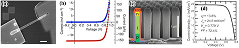
Figure 17. (a) SEM image of a single GaAsP core/shell NW SC. (b) I–V characteristics under dark (blue dots) and AM1.5G illuminated conditions (red dots) of the SC shown in (a) [303]. (a) and (b) are adapted by permission from Macmillan Publishers Ltd: Nature Communications, copyright 2013. (c) SEM image of the InP NW array SC. (d) The 1-sun J–V curve for the SC shown in (c) [298].
Download figure:
Standard image High-resolution imageThe hybrid between the polymer and the III–V NW arrays is also a promising combination for SCs. The polymers, with high absorption coefficients (above 105 cm−1) [311], are cheap to make, easy to process, flexible and lightweight. However, most of the polymers have an exciton binding energy which is much higher than the thermal energy, even at room temperature [311–313]. In order to separate charges, the excitons must diffuse to the junction where the exciton dissociation can occur with the assistance of the band offset energy [314]. However, in the polymer, the exciton diffusion length is normally less than 10 nm, while the penetration length of the light is typically more than 100 nm [315, 316]. On the other hand, the III–V NW structure, with large surface-to-volume ratio, could provide large surface area to efficiently contact with the polymer. In addition with the high carrier mobility and affinity in III–V materials, a greatly enhanced efficiency is expected for the NW/polymer combination due to the fast and efficient charge separation. Bi et al demonstrated the effectiveness of using NW structure in the 3-hexylthiophene (P3HT)/GaAs hybrid SC [317]. The SC with GaAs NWs can reach an efficiency of 1.04% (2.6 sun), while the one with the planar GaAs has negligible photovoltaic response. Similar phenomenon was also reported for the poly(3,4-ethylenedioxythiophene):poly(styrenesulfonate) (PEDOT : PSS) [318]. The introduction of GaAs NW can improve the efficiency from 0.29% of the planar GaAs/PEDOT : PSS cells to 5.8%. At present, the polymer/NW hybrid SC has reached an efficiency of 9.2% by using top-down etched GaAs NW/P3HT/PEDOT : PSS heterojunction [319]. In this device, the P3HT has a type-II band alignment relative to GaAs and thus can be used as an electron-blocking layer to enhance the carrier separation. For the bottom-up grown NWs, an efficiency of 4.11% has been achieved by the GaAs NW/poly(3,4-ethylenedioxythiophene) hybridization [320]. Anionic dopants were incorporated in the polymer to tailor the properties, such as the highest occupied molecular orbital level and the polymer conductivity. The doped polymer can lead to the increased open-circuit voltage, enhanced short-circuit current densities and improved polymer/semiconductor interface transport properties.
Compared with the SC, the photoelectrochemical device can directly change the solar energy into chemical energy. This is beneficial for energy storage and transportation. Similar to the SCs, the photoelectrochemical device requires light absorption and charge separation, which are the strengths of the III–V NWs. In addition, in order to split water into H2 and O2, the photocatalyst conduction band minimum should be more negative than the reduction potential of Ht/H2 (0 V versus normal hydrogen electrode (NHE)) and the valence band maximum needs to be more positive than the oxidation potential of O2/H2O (1.23 V versus NHE) [321]. Moreover, unlike for SCs which prefer maximized output voltage and current, the water splitting device only needs a minimum operating voltage which is enough to cover the sum of the thermodynamic minimum required potential difference, the resistance losses of electrolytes, and any over potentials required to drive water splitting [322]. With that it can maximize the photocurrent density and get the highest solar-to-hydrogen (STH) efficiency. Therefore, the ideal bandgap of semiconductor materials for single-bandgap photoelectrode should be large enough (>1.6 eV) to split water and small enough (<2.4 eV) to absorb a wide range of the solar spectrum [31]. Considering all those requirements, the III–V material is a strong candidate for water splitting. In addition, the NW structure has large surface-to-volume ratio, which provides large surface area for the carrier transfer and the solar-to-fuel chemical reaction. Therefore, the NW structure can reduce the electrochemical overpotential required for the reaction [30, 31]. It has been demonstrated that the introduction of 1.5 μm InP NWs with 3% filling fraction can improve the InP bulk efficiency from around 4% to 6.4% (100 mW cm−2 under AM 1.5G illumination) [323].
At present, the research on water splitting using III–V NWs is focused mainly on the materials GaAsP, InP and InGaN due to their suitable band structure [321, 323–332]. Basically, they can be divided into two categories, with and without a p–n junction. The ones without p–n junctions extract the photo-generated carriers by a junction naturally formed between the semiconductor NW and its surrounding liquid electrolyte [321]. The potential difference between the two sides of the junction drives the flow of the carriers. This can naturally avoid the contact fabrication difficulties in SCs caused by the special nanoscale 1D columnar structure [333]. In this case, the NW surface Fermi level can greatly affect the device performance. Kibria et al presented that the quantum efficiency of their water splitting devices can be enhanced by more than two orders of magnitude by tuning the surface Fermi level of the GaN NWs through controlling the Mg-dopant concentration [332]. The efficiency of water splitting devices could be enhanced by using multi-junction structure. A wafer-scale solar-to-hydrogen conversion efficiency of 0.5% was demonstrated by the core–shell p–n junction water splitting device with 1.7 eV GaAsP NWs grown on Si [326]. This is the first step towards the combination of 1.7 eV/1.1 eV tandem device, which is predicted to be able to achieve an efficiency of 27% under AM 1.5G 1-sun illumination [31]. So far, water splitting using III–V NW is still a new research area and the device efficiency is quite low. The high-density surface state of NWs is one of the causes, which needs to be passivated. But the aqueous working environment of the device can degrade the stability of the materials [326]. Therefore, most traditional surface passivation methods cannot provide long term protection to the water splitting devices. For example, the InGaP passivation layer for SCs had been proofed to be very effective [303], while its passivation effect deteriorates rapidly in the water splitting devices [326]. In this case, the development of new surface passivation technique is critical for achieving high water splitting efficiency.
4.2. Light emitters
The solid-state light source is well known for its low energy consumption and long lifetime. The III-N materials is one of the best choices for making light emitters, due to their direct band gap and wide wavelength coverage. However, for thin film device, there are quite a lot of limitations, such as the low light extraction efficiency, and the difficulty to reach the green and orange wavelengths [334–338]. Changing the thin film structure into the NW geometry is a promising solution to those bottlenecks. Moreover, the NW emitter is highly desirable for on-chip integrations due to its small size and the good strain relaxation ability. Therefore, much attention has been paid to the development of the III-N NW light emitters, including the light emitting diodes (LED) and the lasers.
In thin film LED structure, the lattice and thermal coefficient mismatch between the epilayers and substrates can lead to high-density non-radiative defects, which can significantly reduce the internal quantum efficiency. In addition, the large difference in the refractive index between the semiconductor and air can lead to strong internal light reflection. There exists a critical angle, beyond which the emitted light cannot escape out of the device. This can lead to low external quantum efficiency [339]. In the case of the NW, it can produce a high-quality crystal with low defect density, especially for the threading dislocations. This can greatly increase the internal quantum efficiency. Moreover, the NW has a nanoscale 1D columnar shape, which can suppress the total internal reflection and provide more pathways for generated photons to escape [32]. In addition, due to the antenna effect, the NW LED can further enhance the light extraction [340]. For example, the light extraction efficiency of a InGaN NW LED was about 4.3 times higher than that of conventional thin film LEDs, even though the active region volume was much smaller [341]. Borgstrom et al also showed that GaAsP QDs inserted in GaP NWs can be an order of magnitude brighter than the self-assembled QDs [32].
The NW LED can enlarge the emission wavelength coverage compared with the thin film structure. The spectral range between 550 and 590 nm is the well-known 'green–yellow gap' in the LED technology and none of the existing semiconductor thin films can be used to make high-efficiency LEDs for this region [338, 342]. Considering the band structure, the direct band gap InGaN is the most promising material to reach this wavelength. However, the strain due to lattice mismatch can increase rapidly with the In content in the alloy. This can limit the In incorporation efficiency and the alloy crystal quality [342]. In addition, the strong polarization effects of the WZ nitride material can induce strong internal electrostatic fields (>1 MV cm−1) in the InGaN wells [342–344]. The fields can spatially separate the electron and hole wave functions, leading to low radiative recombination efficiency [337, 345, 346]. Therefore, the efficiency of the nitride LED is good at the blue wavelength region and drops dramatically at the long wavelength region [342]. In a NW geometry, the strain between the InGaN/GaN NW heterostructure can be significantly reduced. This allows growing thick (tens of nanometre) and high-quality InGaN active region with low internal electrostatic fields, which can cover the full visible wave range. This is in stark contrast to the thin film nitride LEDs, whose QW thickness is normally limited to 2–4 nm [346, 347]. The InGaN/GaN NW LEDs emitting from blue to red have been demonstrated [348, 349]. Moreover, the material band structures can be changed from indirect band gap to direct band gap by controlling the NW crystal structure during the NW growth [16]. Therefore, some indirect band gap materials, such as GaP, can be modified to produce green LEDs.
Due to all these advantages, NW LEDs with various materials have been demonstrated, such as InGaAs, InAsP, InGaN and AlGaN [350–353]. Roughly, they can be divided into two categories, namely the radial core–shell structure and the axial structure. In the core–shell structure, the active region and the carrier confinement layers are grown conformably on the NWs. For example, Tomioka et al constructed a GaAs based NW LED on Si substrate, which consists of an n-type GaAs NW as a core and then sequentially with n-AlGaAs (hole confinement), p-GaAs (quantum well), p-AlGaAs (electron confinement), and p-GaAs shells (the capping layer for ohmic contacts) [354]. In the core–shell LEDs, the active region area can be tremendously increased compared with the thin film structure, which can make a much more efficient usage of the substrate area [355–358]. This can also help reducing current densities at the junction for the same total currents, which would alleviate the efficiency droop problem [338]. By adjusting the composition in the active region, it is able to control the emission wavelength of the LEDs. As reported by Qian et al, the nitride LED has tunable emission from 365 to 600 nm by changing the In content in the InGaN layer (figures 18(a) and (b)) [349]. If the NW sidewall facets are non-polar, such as (1  0 0) m-plane in the nitride, it can avoid the spatial separation of holes and electrons in the sidewall active region due to the absence of the internal electric fields. This can significantly enhance the radiative recombination efficiency. Ra et al fabricated the coaxial InGaN/GaN multiple quantum well LEDs. Compared with the thin film LED, their coaxial NW LEDs have a lower onset voltage (2.65 versus 2.9 V), better rectification and higher external quantum efficiency (27.94% versus 18.87% at 50 mA) (figures 18(c) and (d)) [352].
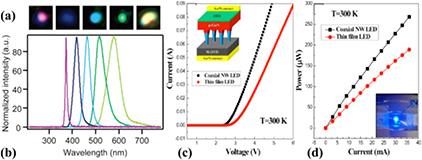
Figure 18. (a) Optical microscopy images collected from around a p-contact of core–shell InGaN NW LEDs in forward bias, showing from purple to yellow emission, respectively. (b) Normalized electroluminescence (EL) spectra recorded from five forward-biased core–shell InGaN NW LEDs with different emission wavelengths. (a) and (b) are reprinted with permission from [349]. Copyright 2005 American Chemical Society. (c) I–V characteristics and (d) the EL intensity of the coaxial p-GaN/ /GaN MQW/n-GaN NW LED as a function of injection currents. Adapted with permission from [352]. Copyright 2013 American Chemical Society.
Download figure:
Standard image High-resolution imageThe axial structure LED has the active region stacked along the NW axial direction, such as the dot/well/disc-in-a-wire structure [359]. This structure is more favourable for contact fabrication and design, because the active region is far away from the contacts. Kikuchi et al demonstrated a novel NW LED structure with a merged tip, which can enable p-type electrodes to be fabricated by the traditional contacting method but keep the superior optical properties of the isolated NW active region [360], as shown in figure 19. This LED showed clear rectifying behaviour with a turn-on voltage of 2.5–3.0 V at room temperature, a forward current of 10 mA (5 V) and a reverse current about 400 μA (−5 V). Similar work was also reported by Bavencove et al [361]. Moreover, the axial geometry is also beneficial for the controllable injection of carriers into the precisely defined active region, which has been demonstrated in the axial p-InP/i-InAsP/n-InP single quantum-dot (QD) NW LED [350]. On the other hand, the surface depletion of the NW can be fatal for the axial-structured devices, because they cannot only lead to high non-radiative recombination rate, but also to space-charge limited transport and high series resistance [362]. Scofield et al showed that by introducing an InGaP surface passivation layer, the axial n-GaAs/i-InGaAs/p-GaAs LED can reduce the series resistance from >1 MΩ to 165 Ω and increase the rectification ratio from 2.5 × 10² to 106 at ±1 V [350]. Moreover, the surface state can significantly reduce the carrier injection efficiency. Nguyen et al introduced an AlGaN shell to passivate the axial InGaN NW LED and increased the output power by more than 2 orders [363]. As the thin film LEDs, the overflow of carrier from the active region can also significantly affect the efficiency of the NW LEDs. But the axial NW LEDs possess more freedom in the barrier material choice, which is benefited from the greatly reduced lattice matching requirements of axial heterostructures. Scofield et al adopted the lattice mismatched GaAsP, rather than the lattice matched AlGaAs, as the n- and p-carrier confinement barriers in the axial GaAs-based NW LEDs [364]. Those LEDs circumvented the side effect of the Al and demonstrated a five-fold increase in output intensity compared with the ones without the barriers.
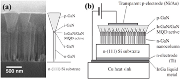
Figure 19. (a) Cross-sectional SEM image of axial InGaN/GaN MQD NW LEDs with a merged p-type top layer and schematic diagram of a single NW LED. (b) Illustration of the LED device structure design with the use of NWs in (a). Reprinted with permission from [360]. Copyright 2004 The Japan Society of Applied Physics.
Download figure:
Standard image High-resolution imageSolid-state white light illumination is an important application of the NW LEDs. In traditional thin film LEDs, the white light is achieved by polychromatic light mixing, e.g. red, yellow, green, blue [365–367]. Due to the 'green–yellow gap' [338], the monolithic white LEDs are typically realized by using yellow phosphors to down-conversion blue light into green light, resulting in limited efficiency and colour rendering [368]. In addition, the most suitable material for fabricating white LEDs is the nitride. In those LEDs, the carrier screening of internal electrostatic fields with increasing drive current can cause a blue shift in the emission wavelength and hence the white colour quality [369]. The NW LEDs can potentially solve the 'green–yellow gap' issue by producing high-efficiency phosphor-free white LEDs. Moreover, the excellent strain relaxation ability can greatly alleviate the internal electrostatic fields, which can significantly mitigate the spectra shift during the current change. Lin et al integrated vertically polychromatic InGaN nanodisc ensembles in the nitride NW LEDs and achieved natural white (colour temperature ~6000 K) emission [370]. This colour temperature is very close to the 5000 K of the sunlight and suitable for daily lighting in our life. The wavelength shifts of each peak in the emission spectra are all smaller than 2.4 nm during the change of injection current from 5 to 25 mA, which indicates the insignificant effect of the internal electrostatic fields on the active region. In addition, they did not observe the deep-defect-related yellow photoluminescence or electroluminescence emission in the NW LEDs commonly accompanying the thin film nitride LED. This could be due to the high crystal quality of NWs. Similarly, Nguyen et al stacked axially 10 InGaN QDs with different emission wavelengths in nitride NWs and achieved phosphor-free white-light-emitting diodes [371]. The correlated colour temperature of the LEDs was around 4500 K with the nearly unaltered CIE chromaticity coordinates ( and
and  ) with increasing the injection current from 100 to 400 mA. Moreover, their LEDs show an internal quantum efficiency of ~56.8% at 200 A cm−2 (300 K) and a virtually zero efficiency droop at current densities up to ~640 A cm−2 (5 K). Later on, the same group improved their phosphor-free white light LEDs by introducing a p-doped AlGaN electron blocking layer between the active region and the p-GaN section to prevent the electron overflow [372]. The LEDs can have virtually zero efficiency droop at current densities up to ~2200 A cm−2. Under injection current from ~333 A cm−2 to 1100 A cm−2, the CIE chromaticity coordinates were highly stable with the values of x and y in the ranges of ~0.33–0.35 and 0.36–0.38, respectively.
The 1D columnar feature of the NWs provides favourable conditions for NW lasing. The semiconductor NW has a large refractive index difference with its surrounding dielectric environment, which enables photonic confinement in the NW cavities [2]. Their sidewalls can be atomically smooth which allow photons to propagate along the NWs with low losses. In addition, the end facets of NWs are also shown to be able to form a Fabry–Pérot-type cavity [373, 374]. Therefore, the NWs can act as waveguides, optical cavities and gain media at the same time for light amplification [33, 34, 375]. The large overlap between the photonic mode and the semiconductor gain media gives the NW cavities high optical gain. Taking together the high optical gain, the small device volume, and strong carrier confinement, the NW lasers have a potential for high efficiency, low threshold, low power consumption, high integration density, high modulation speed. It could have superior performance in high-speed communications, information processing, and optical interconnects, compared with the traditional thin film lasers [376, 377]. Therefore, NW lasers with various structures have been demonstrated [378]. Here, we address the control and adjustment of some important NW laser parameters.
The emission wavelength of the NW laser is an important parameter for its applications. The combination of various materials is the commonly used method of controlling the laser emission wavelength, such as GaN, GaAs, InP, and GaSb [379–383]. However, in order to fine tune the emission wavelength, an alloy with tunable compositions is more preferable. Lu et al achieved a broadband tunable laser emitting in the full visible spectrum (from blue ~470 nm to red ~640 nm) by adjusting the In in the InGaN NWs (figure 20(a)) [384]. Qian et al also demonstrated the colour tunable NW lasers by using lateral multi-quantum wells (MQW) [385]. Their laser optical cavity is a GaN core NW and the gain medium is the InGaN/GaN MQW shells. By adjust the In composition in the MQW, the NW laser emission can be tuned from 365 to 494 nm (figure 20(b)). The recent rapid progress in the ternary NW research, such as the GaAsP, InAsP, InAsSb and GaAsSb [107, 109, 155, 386], could accelerate the development of composition tunable NW lasers. Moreover, in the photonic crystal lasers, tuning the lasing wavelength can be achieved by adjusting the photonic band gap via controlling the NW pillar pitch and diameter. For example, Scofield et al demonstrated the wavelength adjustment from 960 to 989 nm in their GaAs-based NW photonic crystal lasers [387].
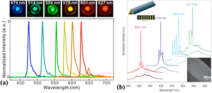
Figure 20. (a) All-colour, single-mode lasing images observed from single InGaN NWs with an emission line width ~4 nm. Reprinted with permission from [384]. Copyright 2014 American Chemical Society. (b) Different wavelength lasing by adjusting the In content in the quantum well of the GaN/InGaN core–shell NW lasers. Insets show the illustration and TEM image of the quantum region, respectively [385]. Reprinted by permission from Macmillan Publishers Ltd: Nature Materials, copyright 2008.
Download figure:
Standard image High-resolution image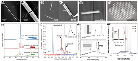
Figure 21. (a) and (b) SEM images of a cleaved-coupled GaN NW. (c) Spectrum from the coupled cavity (blue line) shown in (a) and (b), and each separated component [388]. Copyright 2013 National Academy of Sciences, USA. (d) SEM images of individual GaN NWs. (e) SEM images of coupled GaN pairs by using NWs in (d). (f) Lasing spectra from NWs in (d) and (e). (d)–(f) are reprinted with permission from [390]. Copyright 2012, AIP Publishing LLC. (g) SEM images of a NW coupling with the distributed feedback grating. (h) Lasing spectrum obtained when the GaN NW is perpendicular and parallel to the grating, respectively. (g) and (h) are reprinted with permission from [391]. Copyright 2014, AIP Publishing LLC. (i) SEM images of a InGaAs photonic crystal laser. (j) Lasing spectra of photonic crystals with different NW pitches and diameters. (i) and (j) are reprinted with permission from [387]. Copyright 2011 American Chemical Society.
Download figure:
Standard image High-resolution image
The monochromaticity of the NW laser is highly important for the applications, such as digitized communication and signal processing. However, most NW lasers have multiple frequencies, due to the longitudinal modes native to simple Fabry–Pérot cavities [388]. This can lead to both temporal pulse broadening and false signalling because of group-velocity dispersion. Controlling the dimension of the NW is a straightforward method to adjust the lasing mode between the multi-modes and single mode [389]. As has been demonstrated in GaN NW lasers, the single mode lasing can be achieved by keeping the small NW length (100–250 nm) and the diameter (30–56 nm) [384]. But at this small size, the optical loss is significant and the grain is small. Therefore, it needs a better optical confinement scheme to improve the gain, such as surface plasmons. Coupling NW cavities is an effective way to achieve single-mode emission without reducing the cavity size. When two sets of Fabry–Pérot modes interact coherently with each other, the Vernier effect can select the modes which are sharing the same frequencies [388]. Gao et al coupled two NW Fabry–Pérot cavities axially via an air gap and demonstrated the single-wavelength room-temperature lasing (figures 21(a)–(c)) [388]. They also found that the coupled laser has a lower threshold gain than that of the single cavity NW laser. Xu et al coupled a pair of NW cavities by placing two NWs side-by-side and in contact with each other (figures 21(d)–(f)) [390]. This coupled cavity pair also demonstrated efficient mode selection and achieved single mode lasing. Except changing the laser cavity, the single mode lasing can also be achieved by coupling the NW with its surroundings. Wright et al coupled externally the GaN NW to a dielectric grating and achieved the single mode emission by controlling the grating periodicity and the angular alignment between the NW and the grating (figures 21(g) and (h)) [391]. Moreover, the single mode lasing can be achieved by using a photonic crystal cavity. Scofield et al achieved photonic crystal lasers by growing GaAs NW arrays with InGaAs insertion on patterned substrates (figures 21(i) and (j)) [387]. The lasers show single-mode lasing at room temperature with a low threshold pumping power density of ~625 W cm−2.
The miniaturization of NW laser is important for the high-density on chip photonic and optoelectronic device integration. However, the diffraction limit only allows the dimension of NW lasers to be reduced to half of the operating wavelength [11]. To further miniaturize the NW laser to deep-sub-wavelength scales, an advanced optical mode confinement scheme is needed [11]. The surface plasmonic modes are highly confined, which can help NW lasers to realize ultra-low lasing thresholds and hence reduce the size [11]. Lu et al coupled small InGaN NWs (100–250 nm in length and 30–50 nm in diameter) with an Al2O3-capped Ag film and achieved lasing with ultrasmall thresholds at 7 K (green and red nanolasers ~100 W cm−2, and the blue nanolaser <10 W cm−2) [384, 392]. Ho et al also realized plasmonic GaAs NW lasers with a sub-diffraction limit diameters of ~150 nm and an ultra-low threshold of 1.0 kW cm−2 at 8 K [393].
Only recently, Frost et al demonstrated the first electrically pumped edge-emitting nitride NW array laser [394]. For single NW, the realization of the electrically injected NW laser is still challenging. There are a lot of technology obstacles needed to be overcome, especially the difficulty of realizing effective surface passivation and fabricating reliable nanoscale metal–semiconductor contacts [2].
5. Conclusion and outlook
In the present paper, we have reviewed the advantages, challenges and the breakthroughs of the III–V NW synthesis and their applications in the optoelectronic area. Compared with traditional thin film structures, the NW can facilitate high-quality material integration, due to its efficient strain relaxation ability. The substrate choice can be greatly enlarged, which has been demonstrated in the integration of different material systems with large lattice and thermal expansion coefficient mismatch, such as growing InAs NWs directly on a Si substrate. With further development of the NW technique, it is likely to beat the limitations of the traditional thin film epitaxy, which needs a crystal substrate to provide the growth matrix. For example, it is possible to grow the NWs on non-crystal graphene-treated substrates. During the growth, due to the nanoscale 1D structure and the special growth modes, NWs can have the extra freedom to choose the crystal structure between WZ and ZB, which is difficult to achieve in traditional thin film growth techniques. This can serve as a platform to understand the fundamental properties of materials, and hence likely lead to new discoveries and applications. Especially, the different band structure between the WZ and ZB crystal phases can provide more freedom in the device structure design, such as the crystal-phase quantum dot. For Au-catalysed growth, the crystal phase control has comparatively well developed. For example, it has been demonstrated in InAs NWs that the ZB/WZ phase superlattice with eight bilayers in each phase can be controlled with an accuracy of 98% over 60 periods [395]. On the other hand, for the self-catalysed growth, the crystal phase control is more difficult due to the narrow growth window. For example, most of the reported self-catalysed InAs NWs are still accompanied with high density of stacking faults. Moreover, the growth mechanism, for both Au- and self-catalysed NW growth modes, is still unclear, which adds significant difficulties in controlling the crystal structure. Therefore, more research is needed on NW growth. In addition to the crystal phase, the advanced NW structure, such as axial and coaxial junctions, has also been demonstrated to be able to provide new quantum structures for devices. For example, a QD can be formed, without the assistance of strain, by axial junctions or by phase segregation. However, there are still some difficulties needed to be solved in the control of these advanced structures, such as the 'kinking issue' in the axial heterojunction growth. In the application aspects, NWs are predicted to be superior in optoelectronic area compared with the traditional thin film devices, such as the potential for higher efficiency and lower cost. However, the performance of the present NW devices is still inferior to their thin film counterparts at the moment. In particular, the single NW laser fabricated by the bottom-up approach is still at the optical pumping stage and has not achieved the electrically driven devices yet. Although there are many challenges needed to be overcome in the next few years, such as realizing effective surface passivation and fabricating reliable nanoscale metal–semiconductor contacts, the III–V NW devices are positioned to be the next-generation technology with good functionality, super performance, high integration and ultra-low cost.
Acknowledgments
The authors acknowledge the support of Leverhulme Trust. H Liu would like to thank The Royal Society for funding his University Research Fellowship.