

Abstract
The electronic properties of unstrained unrelaxed InAsxSb1−x alloys have been determined in a wide range of alloy compositions using IR magnetospectroscopy, magnetotransport and IR photoluminescence. All studied alloys have n-type background doping with electron concentration decreasing with the Sb content. The composition dependence of the background doping concentration follows an empirical exponential law in a wide range of compositions. Both bandgap and electron effective mass dependence on alloy composition exhibit negative bowing reaching lowest values at x = 0.63: Eg = 0.10 eV, m* = 0.0082 m0 at 4.2 K. The bowing coefficient of 0.038 m0 obtained for the electron effective mass is in good agreement with that obtained from the Kane model.
Export citation and abstract BibTeX RIS
I. Introduction
Having the lowest bandgap among all III–V semiconductors, InAsxSb1−x alloys attract attention both for fundamental research as a material for possible realization of nontrivial topological phases [1] and as a potential alternative to HgCdTe for long-wavelength infrared (LWIR) optoelectronics [2–7]. The alloy bandgap depends nonlinearly on the composition, and in a certain composition range, the bandgap of the ternary InAs1−xSbx alloy is lower than the bandgap of binary compounds [8, 9]. A complication for wide application of this material in LWIR electronics is that the lattice constant depends strongly on the composition and that no binary lattice-matched substrates are available other than for (Sb) = 9% which matches GaSb. However, the recent development of a special graded buffer layer which accommodates the large difference between the lattice constant of the substrate and the alloy [10] made it possible to obtain high quality unstrained unrelaxed InAs1−xSbx [11, 12]. Experimental analysis of the composition dependence of the electronic properties of these new materials is not only important for the device applications but allows an insight into fundamental aspects of the physics of semiconductor alloys.
The electronic properties of ternary alloys are commonly described within virtual crystal approximation (VCA) approach [13], where the disordered alloy is modeled by an ideal crystal with an average potential at each sublattice site. The average potential is built by linear interpolation of the potentials of corresponding binary materials. A nonlinear composition dependence of the bandgap is obtained within VCA due to the nonlinearity of the band energies as functions of the crystal potential. The nonlinearity of the composition dependence of the InAs1−xSbx alloy bandgap is described by the bowing parameter C:

Positive bowing parameter correspond to negative bowing which means that the real value of the alloy bandgap is less than that obtained using linear interpolation. Earlier experimental bandgap bowing coefficients obtained in different composition ranges gave values varying from 0.58 to 0.7 eV [9]. However, recent analysis of photoluminescence (PL) spectra of bulk unrelaxed InAs1−xSbx alloys for x up to 0.45 gave the bowing parameter of 0.87 eV [8].
Qualitatively, the bandgap bowing can be obtained in the framework of VCA, but the calculated value C = 0.008 eV [14] is much less than the experimental values. To explain the large bandgap bowing, the VCA has to be modified by adding the random potential due to fluctuations of the alloy composition [14, 15]. It is now commonly accepted that the alloy disorder is responsible not only for the large bandgap bowing in the InAsSb system but also determines the composition dependence of most electronic parameters such as carrier effective masses and mobilities [16, 17].
Bouarissa and Aourag [18] calculated the composition dependence of the electron effective mass in InAs1−xSbx alloys using the pseudopotential method which is based on an improved VCA approach, and includes the effective potential due to alloy disorder. A strong negative bowing with the coefficient of 0.025m0 was obtained. This is slightly different from the value of 0.035m0 recommended by Vurgaftman et al [9]. The recommendation is based on the analysis of relatively scarce experimental data and the assumption that the bowing of the electron effective mass was determined entirely by the bowing of the bandgap (see [9] and references therein). Here we present a systematic study of unstrained unrelaxed InAs1−xSbx alloys in a wide range of compositions, which makes it possible to directly measure the bowing coefficients for bandgap and electron effective mass as well as background carrier concentration, which determine the electronic properties of these materials.
We examined unstrained unrelaxed InAs1−xSbx alloys (x = 0.09, 0.22, 0.44, 0.63) using infrared (IR) magneto-spectroscopy, magnetotransport and IR PL experiments. We found that in a wide range of compositions the bandgap and the electron effective mass demonstrate negative bowing with the coefficients 0.83 eV and 0.043 m0, respectively. The alloy with x = 0:63 has the lowest bandgap of Eg = 0.10 eV with a band edge effective mass of 0.0082 m0. To the best of our knowledge, these are the lowest values ever reported for any III–V semiconductor system. The background doping is n-type and the electron concentration increases with the As composition.
II. Experiment and samples
A series of InAs1−xSbx samples with varying Sb concentrations were grown by solid source molecular beam epitaxy (MBE), VEECO GEN930 on undoped GaSb(1 0 0) substrates. Schematic band diagram of the sample with x = 0.44 is presented in figure 1. The 500 nm, p-type −1 × 1016 cm−3 GaSb:Be buffer layer was grown at 530 °C with a V/III ratio ~1.5. 1 μm thick InAs1−xSbx layers were grown at temperature exceeding 1 × 3 to 1 × 5 transition point of surface reconstructions by 10 °C. Compositionally graded 3–4 μm thick InGaAlSb buffers were grown to accommodate lattice mismatch between InAsSb and GaSb substrate. The buffers were grown at 460–500 °C with a V/III ratio ~2.5. AlInSb barriers were grown on both sides of the InAsSb layers. A 100 nm thick InAsSb cap was grown on top of the structure to prevent oxidation of the AlInSb barries. High resolution x-ray diffraction analysis confirmed excellent match of the AlInSb/InAsSb/AlInSb structure to the in-plane lattice constant of the top part of the graded buffer. A cross sectional transmission electron micrograph of the heterostructure with graded buffer and InAsSb layers demonstrated complete confinement of the misfit dislocations in the graded buffer while there was no visible threading or misfit dislocations in the InAsSb [8, 11]. In total 5 InAs1−xSbx structures of different composition (x = 0.09, 0.22, 0.44, 0.63) were grown. Samples with x = 0.09; 0.22, and one sample with 0.44 were n-doped (Te). Two samples with x = 0.44 and x =0.63 were grown without intentional doping. The actual doping concentration of ~6 × 1016 cm−3 was determined by magnetotransport measurements. To avoid formation of 2D electron 'pockets' due to band bending at the boundaries of InAsSb layer the barriers and cap were p-doped to 1016 cm−3. A table of all measured samples and their carrier concentrations are shown in table 2.
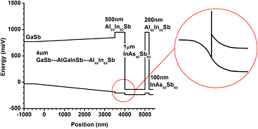
Figure 1. Band diagram of the structure with InAs60Sb40 absorber at T = 4 K. The inset shows the expected band bending at the boundaries of the absorber.
Download figure:
Standard image High-resolution imagePL spectra were measured using setup which includes closed cycle cryostat, FTIR and liquid nitrogen cooled MCT detector. An active Q-switch Nd:YVO3 laser emitting at 1064 nm was used as a pumping source.
Magnetotransport measurements were done on 2.4 mm long and 200 μm wide Hall bars. Ohmic contacts were fabricated by deposition of Ni/Au/Ge/Ni/Au layers and rapid thermal annealing at 250 °C. The cap and top barrier layers were etched down at the contact areas before the contact deposition.
IR transmission spectroscopy measurements were performed in the Faraday configuration at 4.2 K in magnetic fields up to B = 10 T. The spectra were recorded by a Bruker Fourier-transform IR spectrometer with a resolution of 6 cm−1. The IR radiation from either a Hg lamp or glow bar was delivered to the sample via evacuated light pipes, and the intensity of the transmitted light was detected by a composite Si bolometer mounted beneath the sample.
The samples were wedged to reduce the Fabry–Perot oscillations. Spectra acquired at fixed magnetic field are normalized by the zero field transmission, T(B) = T(0), so that the interband (transitions between valence band and conduction band Landau levels) and intraband (CR-like transitions between adjacent Landau levels in the conduction band) transitions show up as a dip in the normalized spectra.
III. Results and discussion
The carrier concentration in InAsSb layers was determined from Shubnikov-de-Haas (SdH) and Hall measurements at 4 K. The dependence of the diagonal component of the magnetoresistivity tensor on the magnetic field is shown in figure 2(a). The carrier concentration was determined from the SdH oscillation period Δ(1/B) according to
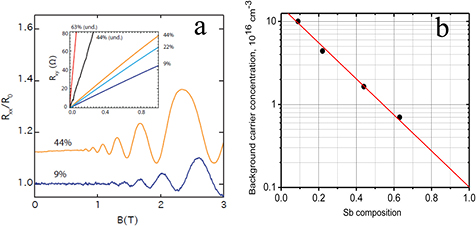
Figure 2. (a) Longitudinal magnetoresistance normalized by the zero field resistance up to B = 3 T showing quantum oscillations for samples 1 (x = 0.09) and 3 (x = 0.44). The curves are shifted for clarity. (b) Background carrier concentration as a function of Sb composition x. The straight line is the fitting with ![$n\left[{{10}^{17}}\,\text{c}{{\text{m}}^{-3}}\right]\,=1.5{{\text{e}}^{-\frac{x}{0.2}}}$](https://content.cld.iop.org/journals/0022-3727/49/10/105101/revision1/daa1063ieqn015.gif)
Download figure:
Standard image High-resolution imageEquation (2) does not contain the effective mass and holds both for parabolic and nonparabolic Kane dispersion [19]. The electron concentration was also extracted from the slope of the magnetic field dependence of the Hall resistance (figure 2(a), inset). SdH electron concentrations are in good agreement with those obtained from Hall measurements. The 3D character of the carriers was confirmed by SdH and Hall measurements in tilted magnetic field. The results of the magnetotransport measurements are summarized in table 1.
Table 1. Doping types and carrier concentrations of the structures.
| Sample | 1 | 2 | 3 | 4 | 5 |
|---|---|---|---|---|---|
| Doping type | n | n | n | undoped | undoped |
| Sb content (%) | 9 | 22 | 44 | 44 | 63 |
| SdH concentration (cm−3) |  |
 |
 |
 |
— |
| Hall concentration (cm−3) |  |
 |
 |
 |
 |
| Background concentration (cm−3) |  |
 |
 |
 |
 |
The discrepancy between the Hall and SdH concentrations is slightly higher for the samples with lower carrier concentrations. This is an indication of the shunting effect of the p-type layers of the structure, since the carriers in these layers contribute to the total Hall voltage but do not change the SdH period of the electrons. The doping concentration of ~6 × 1016 cm−3 was determined as the difference between the electron concentration of the n-doped sample 3 and the undoped sample 4 with the same Sb content. The background concentration was calculated as the difference between the doping concentration and the measured electron concentration. We found that all samples have n-type background doping which correlates with the As content and is the highest for lattice matched to GaSb sample 1 with 9% of Sb (figure 2(b)). The dependence of the background carrier concentration on the Sb composition follows the empirical expression:

Since all the samples were grown at the same temperature, the exponential character of this dependence may indicate a dependence of the activation energy for defect formation on the material composition [20].
The bandgap of the InAs1−xSbx samples were extracted from the magnetic field dependence of the interband light absorption [21, 22]. This method is regarded as one of the most direct methods to measure bandgap [23]. The dependence of the interband magneto absorption spectrum on the magnetic field for samples 3 and 4 is presented as a color plot in figures 3(a) and (b). The dependence is obtained by dividing the absorption spectrum at a given magnetic field by the zero-field absorption spectrum. The red lines are identified as the optical transitions between the ground electron and hole Landau levels. The line curvature is the effect of a strong nonparabolicity of both the conduction and valence bands. The bandgap energy is obtained from the energy axis intercept of these lines. The dependence of the bandgap energy on the Sb composition (figure 4) demonstrates a strong bowing with the coefficient C ~ 0.83. This is close to the value obtained in [8]. The values of the energy gap obtained from magnetoabsorption measurements are very close to these obtained from the PL peaks (figure 5).

Figure 3. Interband magnetoabsorption as a function of magnetic field and emission quantum energy for samples 4 (x = 0.63) and 3 (x = 0.44). The bandgap energies are marked by white arrows.
Download figure:
Standard image High-resolution image
Figure 4. Bandgap energy as a function of the Sb composition. Dots correspond to the magnetoabsorption data, crosses to the energies of the photoluminescence lines.
Download figure:
Standard image High-resolution image
Figure 5. Photoluminescence spectra from InAsSb layers with different compositions.
Download figure:
Standard image High-resolution imageThe electron cyclotron effective mass  was extracted from the energy of the cyclotron resonance absorption peak
  in a low magnetic field (figure 6, inset) using the expression:
where  is the cyclotron frequency. In a narrow gap material with a strong nonparabolicity, the electron effective mass
  at the bottom of the conduction band is, generally, different from the cyclotron mass
  , determined near the Fermi level. High electron concentration and narrow bandgap lead to sufficient difference between
  and
and  . The electron effective mass at the bottom of the conduction band can be obtained from the cyclotron mass using the Kane dispersion relation [19]:

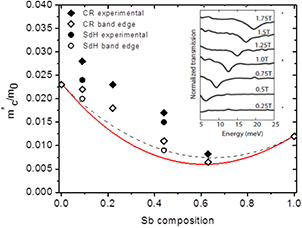
Figure 6.  extracted from cyclotron resonance absorption (solid diamonds) and from temperature dependence of the SdH oscillation amplitude (solid circles) as a function of the Sb composition. Hollow circles and diamonds correspond to the values of
  at the bottom of the conduction band. The values of for x = 0 and 1 are taken in [5]. The solid line is the dependence of
  as a function of Sb composition calculated from the Kane model. The dashed line is a fit using the bowing parameter 0.037. Inset: cyclotron absorption lines of sample 4 (63% Sb) at different magnetic fields.
Download figure:
Standard image High-resolution image
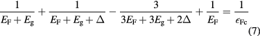
Here Eg is the bandgap, E is the energy, k is the wave vector, P is the Kane matrix element and Δ is the spin–orbit splitting energy. The ratio  can be expressed as:
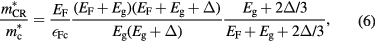
where  and EF is the Fermi energy calculated from the following expression:
Expression (6) is obtained in zero-temperature limit using the assumption that the cyclotron energy  . Since the cyclotron mass was obtained at low magnetic fields, this condition is fulfilled for all samples. The results of the calculations are summarized in table 2.
Table 2. Electronic parameters of the structures.
| Sample | InAs [9] | 1 | 2 | 3 | 4 | InSb [9] |
|---|---|---|---|---|---|---|
| Sb content (%) | 0 | 9 | 22 | 44 | 63 | 100 |
| n (cm−3) | — |  |
 |
 |
 |
— |
 |
— |  |
 |
 |
0.0082 | — |
 |
— | 27 | 33 | 38 | 13 | — |
 |
0.417 | 0.32 | 0.23 | 0.13 | 0.1 | 0.235 |
 |
— | 29 | 37 | 46 | 15 | — |
 |
390 | 324 | 276 | 270 | 374 | 810 |
 |
— | 1.17 | 1.28 | 1.56 | 1.26 | — |
 |
0.026 | 0.024 | 0.018 | 0.011 | 0.0065 | 0.0135 |
The spin–orbit splitting energy Δ was calculated using the corresponding binary parameters  ;
;  [9] using the expression

The bowing parameter is taken as 1.2 eV [9].
For samples 1 and 3 the electron effective mass was obtained from temperature dependence of the SdH oscillations [24, 25]. The masses obtained by this method are slightly less than those extracted from CR absorption spectra. A possible explanation is the effect of free carrier plasma reflection on CR data in the doped samples [26]. The dependence of  on the Sb composition is shown in figure 6. The obtained bowing parameter for the electron effective mass is Cm = 0.038 which is in good agreement with Cm = 0.035 suggested in [9]. This is slightly less than we can expect from the Kane model electron effective mass which is determined by the expression:
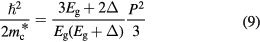
The effective mass bowing coefficient calculated from the Kane model with linearly interpolated (P2) [9] gives Cm = 0.045. A possible reason for the discrepancy is mixing of the conduction and valence band states caused by the random potential due to alloy disorder [16].
IV. Conclusion
Electron effective mass, background carrier density and energy gap of bulk unrelaxed InAsxSb1−x alloys have been determined in a wide range of the alloy compositions using IR magnetospectroscopy, magnetotransport and IR PL. All measured alloys have n-type background doping with electron concentration increasing with the As content. We found that the composition dependence of the background doping follows an empirical exponential law with a characteristic Sb composition of 0.175 in a wide range of compositions. Currently it is not clear whether this exponential law is universal or is a consequence of a particular MBE growth recipe. More detailed study will be published elsewhere. The bandgap energy values extracted from interband magnetoabsorption spectra are close to the PL peak energies and produce a bowing parameter of 0.83. The electron effective mass demonstrates negative bowing with the bowing parameter of 0.038 reaching 0.0065m0 for x = 0.63 which is, to the best of our knowledge, the lowest effective mass ever reported for III–V semiconductors. The obtained bowing coefficient is less than that expected from the Kane model. The difference can be due to conduction-valence band mixing caused by the alloy disorder.
Acknowledgments
The work was supported by US Army Research Office through award W911NF1220057 and by the US National Science Foundation through grant number DMR1160843. J L and D S acknowledge the support by the US Department of Energy, Office of Basic Energy Sciences (Grant number DE-FG02-07ER46451 for IR magnetospectroscopy and magnetotransport experiments and data analysis. The CR and magnetotransport measurements were performed at the National High Magnetic Field Laboratory, which is supported by National Science Foundation Cooperative Agreement number DMR-1157490 and the State of Florida.