

Abstract
We discuss the effect of interlayer insertion into the light absorption region of a carrier escape process for superlattice (SL) solar cells determined by the temperature dependence of photoluminescence (PL) signals. 20-period SL solar cells, with and without interlayers, were prepared. The temperature dependence of the integrated PL intensities due to the transition between quantum levels is well explained by the carrier relaxation models consisting of four processes: radiative and nonradiative recombinations in the SL, thermionic emission to the barrier, and tunnelling after thermal excitation from the lower to the upper levels. We observed that the activation energy for the carrier thermal escaping the quantum well was significantly reduced by the insertion of an interlayer. Moreover, the carrier thermal escaping was also found to be dominant in all processes at 300 K from the calculation of the relevant lifetimes. These results indicate that the insertion of an interlayer results in SL solar cells with a higher efficiency than conventional solar cells.
Export citation and abstract BibTeX RIS
1. Introduction
Multi-junction solar cells accomplish an ultra-high conversion efficiency over a theoretical limit (the Shockley–Queisser limit) [1] of single-junction solar cells. Multi-junction solar cells are composed of p-n junctions of semiconductor materials with different bandgap energies (Eg) to lower the transmission and thermal losses of photoexcited carriers [2]. Currently, InGaP/GaAs/Ge lattice-matched triple-junction solar cells are widely used for space and terrestrial photovoltaics because they are superior to other structures in terms of crystal growth, radiation hardness, and weight [3–5]. However, the total output current of such cells is restricted by the current mismatch caused by the Ge bottom cell generating more current than the other cells. As a solution to this issue, replacement of the Ge cell with other compound semiconductors is expected. Dilute nitride semiconductors, such as GaInNAs, are used in the lattice-matched solar cell. In 2016, an InGaP/GaAs/GaInNAs triple-junction solar cell with a conversion efficiency of 29% at AM0 was reported [6]. However, various crystal defects, relating to the incorporation of a nitrogen atom, reduced the carrier lifetime and diffusion length. As a result, open-circuit voltage and quantum efficiency decreased. Another replacement cell is inverted metamorphic InGaAs [7]. A conversion efficiency of 44.4% was achieved in an InGaP/GaAs/InGaAs inverted triple-junction solar cell under 302 suns [8]. However, the densities of misfit and threading dislocations are very high due to the large difference in the lattice constants of the GaAs and InGaAs cells [3]. Therefore, a compositionally graded buffer layer of several micrometres is required to confine the dislocations in this layer.
The InGaAs/GaAsP multiple quantum well (MQW) structure has the potential to achieve the same lattice constant as that of the InGaP top and Ge bottom cells by balancing the compressive strain in the InGaAs layer with the tensile strain in the GaAsP layer [9]. In addition, the Eg can be controlled by changing the thicknesses and composition of these layers. Therefore, inserting the InGaAs/GaAsP MQW structure into the GaAs cell is also a promising approach to solve the current mismatch loss. In this case, the required Eg for the new middle cell is 1.19 eV [10]. According to Freundlich and Alemu [11], the conversion efficiency of solar cells embedding a QW structure monotonically increases as a function of the well period up to the optimum well period. The reason for the monotonic increase was that the short circuit current increased and the transmission loss was smaller with increasing the well period. In the case of InGaAs/GaAsP MQW structure, a 100-period of QWs is required to optimize the solar cell performance [12]. It was experimentally demonstrated that the conversion efficiency of a triple-junction solar cell with this MQW structure was over 41% [13]. On the contrary, it is well-known that the MQW region acts as a trapping site in carrier transport. Consequently, the performance of this solar cell decreases due to the poor carrier collection issue when a large number of QWs are incorporated to increase the amount of light absorption [14, 15]. Therefore, the key challenge in this structure is how the photogenerated carriers escape to outside the MQW region before carrier trapping occurs.
Recently, a barrier layer with a thickness of several nanometres has been introduced in various MQW solar cells to solve the issue of photogenerated carrier loss [16–18]. Hereafter, we describe such a MQW structure as a superlattice (SL) structure to distinguish it from the MQW structure referred to in the previous paragraph. In a SL structure, electron and hole minibands form along the growth direction, by coupling of the wave functions between adjacent QWs, and carrier tunnelling occurs [19]. Such carrier escaping is expected to improve the carrier collection efficiency. However, the growth of an InGaAs/GaAsP SL structure with a large number of QWs was difficult due to the lattice relaxation caused by the accumulated strain in the SL region [20].
Using the GaAsP barrier layer with a higher phosphorus composition is one of the methods to reduce the strain [18]. The merit of this method is that the carrier escaping by tunnelling is dominant as the thermionic emission to outside of the QW is hampered by the high-potential barrier. On the contrary, a thick well layer is required in order to obtain the optimum Eg for the middle cell. The reason for this being that the higher potential barrier generates a strong quantum confinement effect. This necessitates the extension of the SL region, which may result in the increase of carrier trapping. Therefore, we propose inserting a GaAs interlayer between the InGaAs and GaAsP layers as the strain relaxation layer. This method has two advantages over the structure without the interlayer. Firstly, the interlayer can suppress the strain accumulation and the intermixing of elements between the well and barrier layers [10, 21]. Secondly, it can weaken the quantum confinement effects. This enables the Eg to lower without introducing the compressive strain [10, 12]. In practice, a 100-periods InGaAs/GaAsP SL solar cell with an Eg of 1.23 eV has been accomplished [12].
In addition to the issue of the optimum design of the SL structure, understanding the carrier transport processes in the SL structure must be addressed. Since the potential profile of the conventional SL structure is similar to the MQW structure, except for the thin barrier layer, the carrier escaping processes are the thermionic emission to the outside of the QW and the tunnelling through the barrier layer. The efficiencies of these processes are determined by the thickness and composition of each layer, the temperature and the applied bias [16, 22]. In contrast, the potential profile of the SL structure with the interlayer is more complicated. Moreover, the upper energy levels form in the QW, despite the well layer having the same thickness, due to the weakened quantum confinement effect [10]. In this case, the physical properties of the interlayer, as well as the carrier escaping processes through the upper levels, must be considered. Hence, the carrier escaping processes in this SL structure become more difficult to understand. For this reason, the carrier transport processes in the SL structure with the interlayer have not yet been clarified. In the present study, we investigate the effect of interlayer insertion on the carrier recombination and escaping processes by discussing the temperature dependence of photoluminescence (PL) signal intensities from 4 to 300 K.
2. Experimental procedures
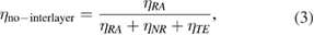
Figure 1 shows schematic illustration and band structure of the measured solar cell samples. The samples were grown on n-type GaAs substrates by metal–organic vapour phase epitaxy (MOVPE). Zinc and sulphur were used as the p-type and n-type dopants, respectively. In general, the carbon atoms contained in the source gas are incorporated in the GaAs layer during the MOVPE process, causing the formation of either a donor or acceptor level depending on the growth conditions such as growth temperature, reactor pressure and V/III ratio [23–25]. Under such growth conditions for the InGaAs/GaAsP MQW, the incorporated carbon atoms acted as unintended acceptors, the electric field in the i region was then weakened by these carriers leading to a low fill factor and external quantum efficiency [26]. However, in the present study, the p-type background doping was compensated by doping a low carrier concentration of sulphur to keep the electric field of the overall i region constant. Although we should prepare the samples with the same well period of QWs to discuss the influence of well period in the carrier escaping process, the 100-period of QWs cannot be grown without an interlayer. Therefore, we used the SL structure consisting of 20-period of QWs for both samples in the present investigation. This structure was inserted into the i region. For the interlayer inserted sample, the thicknesses of the In0.21Ga0.79As well, the GaAs interlayer and the GaAs0.58P0.42 barrier layers were set at 3.8, 3.1 and 2.1 nm, respectively. For the sample without the interlayer, prepared as a reference, the thicknesses of the In0.21Ga0.79As well and the GaAs0.58P0.42 barrier layers were set at 5.1 and 2.0 nm, respectively. The total thickness of the i region was fixed at 1000 nm by changing the thickness of the i-type GaAs layer neighbouring the substrate side of the n-type GaAs. The electric field was calculated to be −12 kV cm−1. After the difference of the Fermi energies in the p- and n-type regions were calculated, the electric filed strength was estimated by dividing this difference by the elementary charge and the thickness of the i region.

Figure 1. (a) Schematic of InGaAs/GaAsP SL samples. The total thickness of the i region was fixed at 1000 nm to keep the built-in electric field constant. The SL structure of (b) interlayer and (c) no-interlayer. (d) Band structure of measured samples. InGaP window layer and valence band of light hole are omitted for simplicity.
Download figure:
Standard image High-resolution imageIn the PL measurements, an argon ion laser (488 nm, 1.3 W cm−2, Spectra-Physics: model 2017) was used as an excitation light source. The sample was set on a cold finger in a cryostat (Sumitomo Heavy Industries: RDK-101D). The excitation light intermittently irradiated the p-type GaAs surface after passing through a mechanical chopper set at 270 Hz. The PL from the sample was dispersed by a monochromator with a 1200 grooves mm−1 grating and was detected with a Si photodiode. The signal-to-noise ratio was improved by applying a lock-in technique. The sample temperature was controlled in the range of 4–300 K by a closed cycle refrigerator.
3. Results and discussion
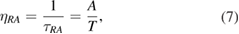
Figures 2(a) and (b) show the PL spectra at 300 and 4 K for the interlayer and no-interlayer samples, respectively. Three PL peaks were observed at 4 K for both samples, which are labelled in the order of energy from lower to higher as A, B and C peaks. Although the A-peak energies changed between the samples with different SL structures, those of the B and C peaks did not change regardless of the sample structure. Therefore, we considered that the A peak was caused by the transition between the quantum levels in the SL structure. On the other hand, the B and C peaks were considered to be related to the electron radiative recombination in the GaAs layer. The broadness of the B peak suggested that this was due to the defect or deep impurity levels in the GaAs layer. Since these electronic states may couple strongly to the lattice, transition energies become much smaller than the energy of the no-phonon transition and at the same time the half width at the half maximum fairly broadens [27, 28].
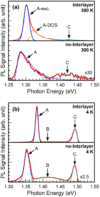
Figure 2. PL spectra of the interlayer and no-interlayer samples at (a) 300 and (b) 4 K. Observed peaks are labelled as A, B and C. The dashed and dotted lines are the fitting curve of each peak.
Download figure:
Standard image High-resolution imageThe temperature dependence of the peak energies is drawn for the interlayer and no-interlayer samples in figure 3. The green solid line in the figure shows the temperature dependence of the Eg for GaAs, calculated from Varshni's empirical expression [29]:

Figure 3. Obtained transition energies as a function of temperature. Those of the interlayer and no-interlayer samples are shown by circles and squares, respectively. The solid line shows the calculated Eg for GaAs.
Download figure:
Standard image High-resolution imageThe transition energies for the observed C peaks decreased with increasing temperature, and these trends were similar to the change of the Eg of GaAs. The ionization energies of the carbon and zinc acceptors in the p-type GaAs layer are 26 and 30 meV, respectively [30]. The position of the C peaks for both samples were in good agreement with the calculated transition energy between the conduction band and these acceptor levels, also indicating that the C peak is caused by the radiative recombination in the p-type GaAs layer.
Next, we focus on the origin of the A peak. Since the PL spectral shape was different for the interlayer and the no-interlayer samples, especially at 300 K as shown in figure 2(a), we consider the effect of exciton formation. For the 2D QW structure, the density of states (DOS) is explained by a step function. The PL emission spectrum is principally expressed as a product of the joint DOS and their carrier distribution for each transition [31] and is given by:
where  is the step function and
  is the critical energy. The additional convolution integral of an emission spectrum with a normal distribution function depending on the measurement system should be included in the fitting procedures. The fitting results for the no-interlayer samples are shown by the dashed curve in figure 2(a). The observed PL spectral shape was well-reproduced by the proposed equation. However, for the interlayer samples, a strong peak below the critical energy was observed. The additional exciton contribution was overlapped to the step function due to the two-dimensional DOS. A Gaussian function was used for the exciton component in the present case, and the observed PL spectra were fitted by these two components. As shown in figure 2(a), we found that the contribution relate to the exciton and the DOS was included; they are drawn by the curves labelled as A-exc. and A-DOS. The reason for the lack of exciton formation in the no-interlayer sample is as follows: it has been reported that the exciton binding energy is decreased by the thin barrier layer [32]. Due to the exciton decay into a free-electron-hole pair by absorption of an acoustic phonon, it is more likely that the exciton is less stable [33]. Since the exponential decay term in equation (2) becomes dominant, the observed PL spectra for the two samples are almost the same at 4 K.
The transition energies between the quantum levels were calculated using a nextnano nanostructure device simulator. The effective mass approximation was used and the Eg shift caused by the strain and electric field was also considered. Material parameters, such as Eg and effective mass, were taken from [26]. The band offset energy between the well and barrier layers was determined by applying the Vegard's law to the valence band maximum energies of InAs, GaAs and GaP, calculated by the first-principle calculation [34]. The band offset energy in the conduction band was estimated to be 329 meV. It was confirmed that the miniband formed at the first electron level (e1) in the no-interlayer sample and at the second electron level (e2) of the interlayer sample. Moreover, the calculated transition energies between the e1 and the first heavy hole levels (hh1) at 300 K were 1.28 and 1.30 eV for the non-interlayer and interlayer samples, respectively, and were in good agreement with the observed values. Therefore, it is also confirmed that the A-peak is due to the radiative recombination from the e1 to the hh1 levels.
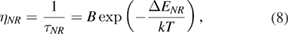
To clarify the carrier transport properties at the SL region, the temperature dependence of the luminescence intensities caused by the transition between the quantum levels are discussed. Figure 4 shows the integrated PL intensities of the A peak as a function of the temperature. The PL intensities were independent of temperature below 100 K for both samples. As the temperature increased, the PL intensity decreased. The thermal quenching rate was larger for the no-interlayer sample than for the interlayer sample. In the present study, we consider the lifetimes of the carrier recombination and escaping processes in the QW. The rate equations are also considered for understanding the temperature dependence of the PL intensity.
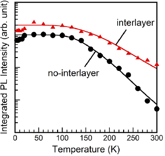
Figure 4. Normalised integrated PL intensities of interlayer and no-interlayer samples as a function of temperature. The horizontal axes are shifted in the vertical direction for clarity. These intensities fit the calculated values from equations (5) and (6), and the fitting curves are represented in the figure.
Download figure:
Standard image High-resolution imageIn our experiment, the light penetration length of the excitation light source was calculated to be approximately 100 nm from the absorption coefficient of bulk GaAs [35]. Since this value is less than the total thickness of the p-type GaAs layer, the excitation light cannot penetrate the SL region. Therefore, the dominant number of electrons are generated in the illuminated p-type region and diffused to the n-type region. So, we considered that the electrons recombine with the hole during capturing in or escaping from the QW. Figure 5 shows schematic models for the carrier transport process in each QW in the SL structure for the no-interlayer (a) and interlayer samples (b), respectively. The dominant carrier recombination processes in the SL structure are the radiative recombination between the quantum levels and the nonradiative recombination related to impurity or defect levels at the hetero junction interface. The e1 electron level in the no-interlayer sample formed the miniband, as discussed above. Three processes for the electrons in the e1 state are considered. They are the radiative,  , and nonradiative recombination,
  , and thermal escaping to the outside of the QW,
  . For the interlayer sample, additional tunnelling through the e2-miniband after thermal excitation from the e1 state to the e2 state,
  , occurs. This is because the e2 electron level formed the miniband, as previously discussed. Detailed calculations are discussed in the followings.

Figure 5. Carrier recombination and escaping processes in (a) no-interlayer and (b) interlayer samples. These activation energies are denoted by the double-headed arrows.
Download figure:
Standard image High-resolution imageThe radiation efficiencies of each sample are obtained by the ratio of the radiative recombination rate to the total rate:
and

Therefore, the dependences of the radiative intensity of each sample are written by:

and

where  is the normalised radiative intensity at 0 K.
Then, we discuss the possible electron transition paths as mentioned above, in more detail. According to Feldmann et al [36], the radiative recombination lifetime of free exciton in the QW was proportional to the product of the Boltzmann constant and temperature. This can, therefore, be described by:
where  is the radiative recombination lifetime and
  is a constant independent of temperature. On the contrary, it is generally known that the nonradiative recombination rate is expressed by the Arrhenius type equation [37]:
where  is the nonradiative recombination lifetime,
  is a constant independent of temperature and
  is an activation energy for the nonradiative recombination.
In the no-interlayer sample, the dominant escaping process in the SL structure with a thin potential barrier is the tunnelling through the miniband. We confirmed that the miniband formed in the e1 level by the theoretical calculations, as previously discussed. The tunnelling rate at the sth sub-band under the application of the electric field is given by [38, 39]:
and

where  is the Planck constant divided by 2
 ,
,  is the band offset energy of the conduction or valence band,
  is the sth sub-band energy,
  is the elementary charge, and
  is the electric field in the i region.
  and
and  are the thicknesses of the QW layer and barrier layer, respectively.
  and
and  are the effective masses of the QW layer and barrier layer, respectively. The pre-exponential and exponential terms in equation (9) indicate the time for the electrons to shuttle between the ends of the QW layer and the transmission coefficient, respectively. However, this process may not significantly contribute to the carrier escaping process outside the QW in the no-interlayer sample. The reason for this is as follows: although the electrons in the SL region can tunnel through the e1-miniband, they have to be thermally excited to escape to the outside of the QW. This is because the energy of the e1-miniband is lower than the conduction band edge of the i-type GaAs layer and the potential barrier becomes too thick for the electrons to tunnel. The theoretical calculation for the band alignment, nextnano, also confirmed the results. Therefore, we considered that the thermionic emission is dominant in the carrier escaping process for the no-interlayer sample as well as the MQW structure with a thick barrier layer. The thermionic emission rate is given by [40]:
where  is the thermionic emission lifetime and
  is an activation energy for the thermionic emission.
In the interlayer sample, however, we found the miniband formed in the e2 level, as shown in figure 5(b). In the present study, we considered the carrier escaping process from the e1 level. This is because the observed PL intensity is only due to the transition from e1 to hh1 levels. In this sample, the miniband formed in the e2 level and the energy is higher than the bottom of the conduction band of the GaAs. This enables the electrons to transport through the e2-miniband to the n region. We neglected the recapture of the carriers in the e2-miniband to e1 level for simplicity. The electrons in the e1 level are prevented from tunnelling by the thick potential barrier consisting of two interlayers and a barrier layer. However, the e2-miniband allows the electrons to tunnel through the barrier once the electrons are thermally excited. Its rate is generally described by the product of the tunnelling rate, shown in equation (9), and the occupation factor of the upper level given by the Boltzmann distribution function [41]. Furthermore, the effect of the inserted interlayer on the effective well thickness and effective mass should be taken into account. The effective well thickness in the e2-miniband  becomes
  where
where  is the thickness of the interlayer. To contrast, the effective mass in the miniband can be calculated from the effective mass and the carrier existence probability in each layer [42]. In the e2-miniband, this is expressed by the following equation:

where  is the effective mass of the relevant interlayers.
  ,
,  and
and  are the electron existence probability in the QW, interlayer and barrier layer, respectively. These probabilities are calculated using nextnano. Accordingly, the rate of tunnelling through the e2-miniband after thermal excitation should be modified as follows:
where  is the lifetime of the tunnelling through the e2-miniband after thermal excitation and
  is an activation energy for the tunnelling through the e2-miniband after thermal excitation.
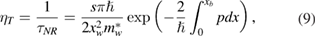
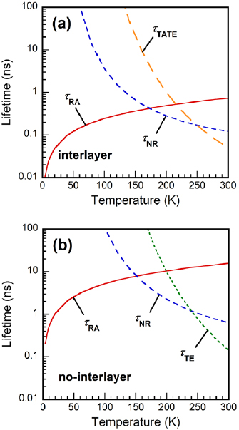
The fitting was carried out using equations (5) and (6), and these results are shown in figure 4 by the solid lines. The composition of the consisting material and their effective masses and carrier existing probabilities are shown in table 1. The fitting parameters for the calculation are also summarised in table 2. The thermionic emission process in the interlayer sample was neglected because of the small contribution and simplicity of calculation. Furthermore, we calculated the lifetimes of each process by substituting the fitting results. This quantitative evaluation helps us to understand what the dominant process in each temperature range is. Figure 6 shows the calculated temperature dependence of the lifetimes. In this figure, the process of the shortest lifetime is the dominant process in each temperature range. We found that the lifetime of the radiative recombination process,  , increased with increasing the temperature for both samples. The drastic increase at a low temperature region suggested that the radiative recombination quenched rapidly with increasing temperature. The nonradiative recombination component,
  , appeared in the mid-temperature region, and the tunnelling through the e2-miniband after the thermal excitation,
  , and the thermionic emission terms,
  , were revealed in the highest temperature region. It is found that the latter two components,
  and
and  , are important for room temperature application of the devices.
Table 1. Material parameters used to fit the integrated PL intensity.
| GaAs0.58P0.42 barrier | GaAs interlayer | In0.21Ga0.79As well | |
|---|---|---|---|
 |
0.093 | 0.067 | 0.057 |
 |
0.14 | 0.71 | 0.15 |
Table 2. Fitting parameters for the interlayer and no-interlayer samples.
| Interlayer | No-interlayer | |
|---|---|---|
 |
1.5 × 10⁻³ | 1.0 × 10⁻³ |
 |
4.1 × 10¹¹ | 1.9 × 10¹⁰ |
 |
4.6 × 10¹⁰ | 2.0 × 10¹⁰ |
 |
0.1 | 1.1 |
 (eV) (eV) |
0.044 | 0.066 |
 (eV) (eV) |
— | 0.208 |
 (eV) (eV) |
0.155 | — |
Figure 6. Calculated carrier lifetimes of radiative, nonradiative, thermionic emission, and tunnelling through the e2 miniband after the thermal excitation for (a) interlayer and (b) no-interlayer samples as a function of temperature.
Download figure:
Standard image High-resolution image
The carrier recombination processes were discussed by considering the ratio of constants in the nonradiative and radiative recombination processes,  , from equations (7) and (8). The increase of
  signifies an increase in the nonradiative recombination component. From table 2, we found the
  were 0.11 and 1.06 for the interlayer and no-interlayer samples, respectively. This result indicated that the PL intensity was suppressed by increasing
  . Since one of the reasons for inserting the interlayer into the QW was the relaxation of the accumulated strain between the well and barrier layers, the nonradiative recombination might be reduced [10]. This is the case for the interlayer sample; the nonradiative contribution became small. However, the activation energy for the nonradiative recombination,
  , for the interlayer sample was slightly smaller compared to the no-interlayer sample. A smaller activation energy usually induces a larger contribution for the electron transition. However, this is not the case. It should be considered that the larger strain results in a larger activation energy for the carriers to carry out the nonradiative transition path. It is indicated that the nonradiative recombination increased due to interface defects produced by inserting the GaAs interlayer. Therefore, manufacturing of the highest quality interface is required for the design of a more suitable interlayer.
Next, we focused on the carrier escaping processes. The observed  of 0.208 eV for the no-interlayer sample corresponded to the calculated potential height of 0.249 eV from the e1 level to the bottom of the conduction band of the GaAsP barrier layer. However, the observed
  of 0.155 eV for the interlayer sample agreed with the calculated transition energy of 0.154 eV between the e1 level and the e2 level. Therefore, it was found that the experimental results could accurately express the carrier thermal escaping process caused by the increased temperature. Moreover, the
  of the interlayer sample was approximately 50 meV lower than the
  of the no-interlayer sample. This decrease showed that the e2-miniband, formed by insertion of the interlayer, enhanced the carriers escaping to the outside of the QW. This was clearly shown in figure 6. The tunnelling through the e2-miniband after thermal excitation dominated in the carrier relaxation process above 250 K, as well as the thermionic emission process, in spite of the increase of nonradiative recombination. As a consequence, we could experimentally demonstrate that the interlayer was an important key to achieve a carrier escaping efficiency higher than the conventional SL structure devices.
4. Conclusions
The carrier thermal escaping process in the SL solar cell with the interlayer was investigated using temperature-dependent PL measurements. To analyse the integrated intensity for the e1–hh1 transition as a function of the temperature, carrier dynamic models in the SL with and without the interlayer were proposed. In these models, the carrier recombination processes were the radiative and the nonradiative recombination for both samples, and the carrier escaping processes were the tunnelling through the e2-miniband after thermal excitation for the interlayer and the thermionic emission for the no-interlayer sample. From the fitting analyses in the integrated PL intensities, the tunnelling through the e2-miniband after thermal excitation caused by the interlayer insertion decreased the activation energy for the carrier thermal escaping. Moreover, the calculated lifetimes for the carrier thermal escaping of both samples at 300 K were the lowest in all processes. We found, experimentally, that the tunnelling through the e2-miniband can help the photogenerated carriers to escape the outside of the QW. We also found that the SL solar cell with the interlayer was superior to the conventional SL solar cell in terms of the carrier thermal escaping efficiency. However, the activation energy for the nonradiative recombination decreased because of the interlayer insertion. In future work, a selection of appropriate interlayer materials will be an important key to develop highly efficient SL solar cells over conventional solar cells.
Acknowledgments
Part of this study was supported by the New Energy and Industrial Development Organization under the Ministry of Economy, Trade and JSPS KAKENHI Grant Nos. 16H04648 and 18K04876.