

Abstract
On-chip optical interconnects heterogeneously integrated on silicon wafers by transfer-print technology are presented for the first time. Thin (<5 µm), micron sized light-emitting diodes (LEDs) and photo diodes (PDs) are prefabricated and transfer-printed to silicon wafer with polymer waveguides built between them. Data transmission with total power consumption as low as 1 mW, signal to noise ratio of >250 and current transfer ratio of 0.1% in a compact volume of <0.0004 mm3 are demonstrated. Experiment shows that the polymer waveguide between the LED and PD plays a key role in enhancing the data transmission efficiency. Reciprocal performance for bidirectional transmission is also achieved. The results show the potential for cost-effective and low profile form-factor on-chip opto-isolators.
Export citation and abstract BibTeX RIS
1. Introduction
Opto-isolators or optocouplers [1, 2] are ubiquitous optical interconnects consisting of light-emitting diodes (LEDs) and photo receivers. They are widely used for optical data transmission between two electrically isolated parts of a circuit operating at very different voltage levels. Although the traditional opto-isolators have been used for more than forty years, their application is limited (such as in printed circuit boards) because of their inefficient device assembly, complex packaging and large form factors. As a result, on-chip applications have not been possible up to now. However, there is an increasing need for signal isolation in complementary metal-oxide-semiconductor (CMOS) circuits [3].
Although on-chip opto-isolators using silicon-on-insulator CMOS technology are being proposed [4, 5], it is wise to integrate silicon with III–V for high-efficiency opto-isolators since III–V and silicon are complementary for photon generation and electronics, respectively. There have been four main methods proposed for III–V/Si integration, including III–V epitaxy on Si [6, 7], III–V flip-chip bonded onto Si [8, 9], III–V wafer or die bonded on Si [10, 11] and III–V transfer-printed on Si [12, 13]. On-chip optical links have been successfully demonstrated by the first three techniques [14–16], but each of them has its own issues, such as the mismatch of lattice constants and coefficients of thermal expansion, difficult optical alignment and inefficient material utilization. Transfer-printing can address these issues being a promising technology for heterogeneous device integration with high scalability and high throughput process. The transfer-printing technology begins with the preparation of arrays of suspended devices supported by tethers on a donor substrate. An elastomeric stamp is used to contact these devices and pick them up quickly, and then transfer them to a receiving substrate releasing the devices slowly, according to the rate-sensitive adhesion between the stamp and the devices [17]. It is being used in advanced micro-LED displays [18], and also with components such as laser diodes (LDs) [19], photodetectors [20], photovoltaic cells [21], ring resonators [22], and single-photon sources [23]. Both GaAs-based and InP-based LDs were integrated on silicon by transfer-printing [19, 24–26], but an on-chip optical link on silicon by transfer-printing has not been reported yet.
In this paper, we demonstrate an on-chip optical link with a simple design where micron-scale InP-based LEDs and photo diodes (PDs) are assembled onto a silicon wafer by transfer-printing and the data transmission is achieved through a spin-coated polymer waveguide butt-coupled to the printed devices. A compact volume of less than 0.4 × 0.2 × 0.005 mm3, current transfer ratio (CTR) up to 0.1%, low power consumption of 1 mW, signal-to-noise ratio (SNR) of over 250 and reciprocal bidirectional transmission are achieved, as we briefly reported recently [27]. The optical coupling efficiency between the LED and PD is enhanced by 60 times using a polymer waveguide. The factors limiting the CTR including the LED in-plane output efficiency, SU-8 waveguide loss and PD responsivity are investigated. The LED in-plane output efficiencies are estimated by a simple model using on-chip LD-to-PD and LED-to-PD interconnects as references, and their low output efficiencies are demonstrated to be the main limiting factor for the CTR of our optical interconnects. Our results demonstrate that the combination of advanced assembly together with microscale high-performance light emitters and detectors will lead to cost-effective miniaturized on-chip opto-isolators.
2. Design
The optical interconnect is designed for on-chip opto-isolators, and a typical opto-isolator usually consists of a light source, an electrically isolated transmission media and a photo receiver. To meet the requirements of low power consumption and low production cost for opto-isolators, LEDs are chosen as the light sources in our design since they have no threshold current, a higher number of devices per unit area and higher production yield than the LDs. PDs are selected as the photo receivers and, in this paper, share the same epitaxial wafer with the LEDs so that the LEDs and PDs can be fabricated at the same time. Although the commercial opto-isolators just use a resin uniformly filled between the large-area LEDs and PDs for both electrical isolation and optical transmission, a waveguide is to be built in our design to enhance the optical transmission efficiency because the light absorption aperture of our on-chip PDs is considerably smaller than that of the surface-illuminated PDs in the commercial opto-isolators. Compared to dielectric (such as SiO2 or SiNx) waveguides, polymer waveguides have the advantages of suitable thickness, low stress and easy fabrication. We choose SU-8 2 (MicroChem) as the waveguide material which can achieve a thickness up to 5 µm and has a high dielectric strength of over 106 V cm−1. This means that even a 10 µm-long SU-8 waveguide can isolate 1 kV. As a result our optical interconnects can be made very compact. Figure 1 shows a schematic arrangement of an optical interconnect arrayed on a silicon wafer.

Figure 1. Schematic diagram of on-chip optical interconnect realized by transfer-printing on a silicon wafer.
Download figure:
Standard image High-resolution imageSince the light-absorptive packaging of the commercial opto-isolators is not used in our design, the light absorption by the CMOS devices in the eventual silicon wafer should be avoided. Thus, the central photoluminescence wavelength of the III–V epitaxial wafer is designed to be around 1550 nm which avoids the light absorption by the silicon. The epitaxial structure is very similar to those of the commercial 1550 nm lasers, except that a 500 nm-thick InAlAs sacrificial layer is inserted between the substrate and the n-doped InP layer to allow the device undercut and separation in the transfer-printing process. Our previous experiments demonstrated that the InAlAs sacrificial layer could be isotropically etched with a higher selectivity to the surrounding InP when compared with an InGaAs sacrificial layer [28].
To make the structure as simple as possible, the mesa of the LEDs is designed to be square with widths of 10 µm, 20 µm and 50 µm. The sidewalls of the mesa, except for the front facet, are coated by SiO2 and metal layers to reflect light towards the front facet. The SU-8 waveguides have a length of 100 µm and are 10 µm wider than the LEDs they connect with. The PDs are rectangular with a length of 100 µm and are 10 µm wider than the SU-8 waveguides they connect with.
3. Fabrication
The epitaxial wafer for the LEDs and PDs is grown by metal organic vapor phase epitaxy on an InP substrate [29, 30]. The epitaxy consists of a sacrificial layer, n-type cladding layer, active region, p-type cladding layer and contact layer. The active region includes six compressively strained AlGaInAs quantum wells and the total thickness is ~100 nm. The total epitaxial thickness is about 4 µm.
The overall process flow of the on-chip optical link is shown in figure 2(a). The III–V sample is firstly patterned with Ti/Au for the p-type metals on the LEDs and PDs, and then mesas are etched into the n-type lower cladding layer by inductively coupled plasma (ICP) to define the LEDs and PDs with an etch depth of ~3 µm. Then Au/Ge/Au/Ni/Au layers are deposited as the n-type contact metals on defined regions of the etched area. After metal annealing, a dielectric film of SiO2 is coated on the surface and mesa sidewalls, and openings to the p-type and n-type metals are made. 400 nm-thick Ti/Au layers are patterned as the probe pads and also the T-shaped alignment marks for the transfer-printing process. LED and PD coupons are defined and isolated by ICP etching through the n-type cladding layer to the top of the sacrificial layer. Grating features are patterned in the sacrificial layer around the coupons as initial etching points for the etching of the sacrificial layer. The coupons are then patterned with a 4 µm-thick resist which acts both to anchor the devices on the InP substrate, and as tethers to support and protect the devices during the undercutting. The sacrificial layer is then fully etched in FeCl3:H2O (1:2). After that, the LEDs and PDs are picked up individually by an elastomer stamp and transfer-printed to a Si target wafer with automatic alignment. The Si target wafer is patterned with alignment marks and pre-coated with a 1 µm-thick polymer (Dow Chemical Intervia 8023) layer for improved adhesion of the printed devices to the wafer. The devices are printed with an alignment accuracy better than ±2 µm. The protective resist and uncovered adhesive polymer are removed with an oxygen plasma etching and the polymer under the devices is then hard-cured at 175 °C. A 2 µm-thick SiO2 is deposited and patterned between the LEDs and PDs for the lower-cladding layer with a length of ~90 µm and widths of over 100 µm. 2 µm-thick SU-8 is used to define the waveguides with a length of ~100 µm on the lower-cladding layer by lithography and cured at 150 °C, as shown in the inset of figure 2(b). The waveguide sidewalls are relatively rough because of the imperfect fabrication of the SU-8 waveguide. Finally, a SiO2 encapsulation is deposited and patterned on the SU-8 waveguides as an upper-cladding layer. The final optical interconnects are displayed in figure 2(b).
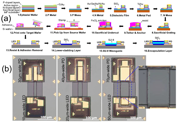
Figure 2. (a) Schematic overview of the fabrication process flow. (b) Optical images of the realized transfer-printed optical interconnects on silicon. The inset in (b) shows a zoom-in view of the SU-8 waveguide between the 50 µm-wide LED and 70 µm-wide PD.
Download figure:
Standard image High-resolution image4. Results and discussion
The measured PD current indicates the response of the optical interconnect. The CTR is a special specification for the opto-isolators, which is the ratio of the PD current divided by the LED current. CTR as an index for system efficiency eliminates the voltage factor affected by the probe resistance, metal/semiconductor contact resistance and other resistances associated with different metal contact sizes. Figure 3 shows the unbiased PD current, LED power consumption and CTR as a function of the LED current for the optical interconnects with 10 µm-wide, 20 µm-wide and 50 µm-wide LEDs. It is seen that the responses of the 10 µm-wide and 20 µm-wide LEDs become quickly saturated with the increasing LED current while that of the 50 µm-wide LED keeps its response efficiency up to a high LED current of 5 mA. This is because the higher current densities for the 10 µm-wide and 20 µm-wide LEDs result in non-radiative Auger recombination that reduces the photon generation efficiencies. Since our PD response currents are in the range from 0.5 µA to 20 µA, the power consumption of the PDs can be ignored, and the power consumption of the interconnects approximates that of the LEDs inside. At the same injection current, the power consumption of the LEDs (and therefore also the interconnect) decreases with the increased LED size since the LED voltage reduces as the metal contact area becomes larger. The power consumption of our interconnect with a 50 µm-wide LED and a PD response current of 0.85 µA is less than 1 mW. As the LED current increases, the CTR of the interconnects initially increases before decreasing at the saturation current densities of the LEDs (~580 A cm−2 for the 10 µm-wide LED). The peak CTR of the interconnect increases and shifts to higher currents as the LED width increases, and reaches 0.09% for the interconnect with the 50 µm-wide LED. Since the CTR value is current-dependent, it is better that the optical interconnects operate at an LED current range where the CTR is maximised and the IPD–ILED curve is linear. From figure 3, this range (termed 'linear operation range' here) of the interconnect becomes wider as the LED size increases. Figures 4(a) and (b) shows the effects of the reverse PD voltage on the PD response current and the dark current, respectively. Reverse voltage from −1 V to −4 V on the PD results in very little improvement in the response, increasing the peak CTR from 0.09% to 0.1%, indicating that nearly all photogenerated carriers are being extracted at zero bias. The dark currents of the PDs are less than 0.1 nA under zero PD bias and increase to only 2 nA even with a voltage of −7 V. Considering that the PD response current is >0.5 µA when the LED current exceeds 1 mA, the SNR of our interconnects is greater than 250.
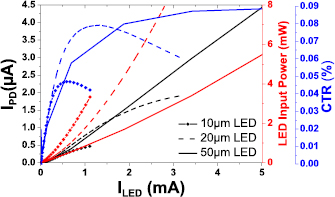
Figure 3. PD response (black lines), LED power consumption (red lines) and CTR (blue lines) for the interconnects with 10 µm-wide (solid lines with symbols), 20 µm-wide (dash lines) and 50 µm-wide (solid lines without symbols) LEDs.
Download figure:
Standard image High-resolution image
Figure 4. (a) PD current and CTRs of the optical interconnect with a 50 µm-wide LED for reverse PD voltages. (b) Voltage-current characteristics for the PDs with different widths.
Download figure:
Standard image High-resolution imageOptical waveguides play a crucial role for high-efficiency light transmission [31, 32]. The guiding effect of our SU-8 waveguides is demonstrated by comparing the results with and without the SU-8 waveguides, as depicted in figure 5. Interconnects with 20 µm-wide and 50 µm-wide LEDs are tested before and after the SU-8 waveguides are fabricated. The responses increase by about 60 times after the SU-8 waveguides are present, indicating that >98% of light collected by the PDs is guided within the waveguides rather than undesirably coupled through the silicon substrate.
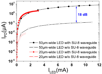
Figure 5. Comparison of PD response between the optical interconnects with and without an SU-8 waveguide.
Download figure:
Standard image High-resolution imageThe loss coefficient of the 30 µm-wide SU-8 waveguide is also studied by comparing three optical interconnects with the 20 µm-wide LEDs and 40 µm-wide PDs but different SU-8 waveguide lengths of 100 µm, 200 µm and 300 µm. Firstly the relationship curves between the CTR and LED current for the three optical interconnects are depicted in figure 6(a) and their peak CTRs with the LED currents all around 1.2 mA are selected. The relationship between the peak CTR and the SU-8 waveguide length can be described as follows:

where α, L, CTR0 and CTRL are the waveguide loss coefficient, SU-8 waveguide length, constant representing the peak CTR with 'zero' waveguide length, and peak CTR with waveguide length of L, respectively. A linear fit between lnCTRL and L is plotted in figure 6(b), and the estimated α and CTR0 are 203 dB cm−1 and 0.126%, respectively. This indicates that the losses including electronic-to-optic conversion loss, butt-coupling loss and optic-to-electronic conversion loss are larger than 99%. Although the calculated SU-8 waveguide loss coefficient is larger than those in the typical laser-to-PD interconnects [14–16], it is not the main factor for the current transfer loss in our interconnects. The large waveguide loss is attributed to the light escape associated with the broad-angle emission of the LED into the limited numerical aperture waveguide, the waveguide scattering and inefficient collection of the light by the PD rather than the absorption since the extinction coefficient of the SU-8 at infrared wavelengths is very low [33].
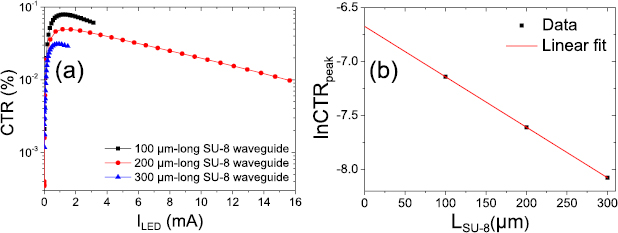
Figure 6. (a) CTR as a function of LED current of the optical interconnects with different SU-8 waveguide lengths. (b) Data and linear fit of the logarithm of peak CTR for different SU-8 waveguide lengths.
Download figure:
Standard image High-resolution imageFor edge-emitting LEDs, it is difficult to precisely measure the in-plane emission power since it is hard to fully collect the light from all emission angles. In order to analyse the output power of our micron sized LEDs, an experiment based on the on-chip coupling between an etched-facet LD and PD is designed to estimate the PD 'responsivity'. LDs with 10 µm ridge width and 500 µm cavity length along with adjacent PDs with 20 µm ridge width and 400 µm length are fabricated as shown in figure 7(a). The sidewalls of the LD ridges have the same etch depth as the facets and are covered with the passivation and metals. The LDs and PDs share the same epitaxy wafer and process flow as our LEDs and PDs, and their interconnect performance is tested on chip. Since the laser light has smaller emission angles and the gap between the LD output facet and PD input facet is as low as 1 µm, the output light from the LD facet, apart from that reflected by the PD facet, is assumed to be totally collected by the PD. The output power of the LD is measured by scribing the sample in front of the etched facet of a ridge LD and collecting the output power from that facet using a commercial photodetector (Newport 883-SL). Figure 8 shows the L–I curve of the ridge LD, IPD–ILD response of the LD-to-PD interconnect and the 'responsivity' of the PD. The L–I curve is measured from the etched-facet LD scribed from the sample while the IPD–ILD response is measured from the on- chip LD-to-PD interconnect. The threshold current (35 mA) calculated from the IPD–ILD curve of the interconnect is very similar to that (36 mA) from the L–I curve of the off-chip LD, which means the reflected light by the PD facet has a very little effect on the LD performance. The 'responsivity' of the PD is calculated by dividing the IPD–ILD curve by the L–I curve. The resulting value for 'responsivity' is 0.54 A W−1 with small fluctuation of ±3% for the LD current range from 50 mA to 80 mA. We should note that this value ignores the optical loss from the PD facet reflection, and thus the actual PD responsivity is underestimated. Groups of on-chip LED-to-PD interconnects are also fabricated as shown in figure 7(b). 10 µm-wide LEDs are coupled to 20 µm-wide PDs and 50 µm-wide LEDs are coupled to 60 µm-wide PDs. Various airgaps from 1 µm to 6 µm exist between the LED output facets and PD input facets to deduce the peak CTR of the LED-to-PD interconnect with 'zero' facet gap. Figure 9 shows the exponentially fitted peak CTR versus facet gap curves of the LED-to-PD interconnects. The deduced peak CTR for 10 µm-wide LEDs coupled to 20 µm-wide PDs with 'zero' facet gap is 0.104%, and is 0.155% for 50 µm-wide LEDs coupled to 60 µm-wide PDs with 'zero' facet gap. Also from figure 6(b) the peak CTR for 20 µm-wide LEDs coupled to 40 µm-wide PDs with 'zero' facet gap (CTR0) is 0.126%. If we assume that, except for the light reflected by the PD facets, all the output light from an LED can be coupled to a PD with 'zero' facet gap, the slope efficiencies of the L–I curves of the LEDs can be calculated by dividing their peak CTR by the calculated PD 'responsivity'. Thus the L–I slope efficiencies of 10 µm-wide, 20 µm-wide and 50 µm-wide LEDs are calculated to be 1.93 mW A−1, 2.33 mW A−1, and 2.87 mW A−1, respectively. Also, the output power of 10 µm-wide, 20 µm-wide and 50 µm-wide LEDs at 250 A cm−2 current density (less than the saturation current density of the LED) are calculated to be about 0.49 µW (ILED = 0.25 mA), 2.33 µW (ILED = 1 mA), and 17.9 µW (ILED = 6.25 mA), respectively. It should be noticed that in this model for the estimation of LED output efficiency and power, some factors are not considered such as the variation of light absorption coefficient of the PDs for different input light wavelengths. Further calibration should be used for more accurate results.
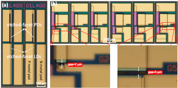
Figure 7. Optical images of (a) the on-chip LD-to-PD interconnects with 1 µm facet gap and (b) the on-chip LED-to-PD interconnects with 10 µm-wide (left) and 50 µm-wide (right) LEDs and different facet gaps. The insets in (b) show the zoom-in views of the coupling regions between the LEDs and PDs.
Download figure:
Standard image High-resolution image
Figure 8. Output power-current (L–I) curve (black line with symbols) of the etched-facet LD measured off-chip, PD current versus LD current (IPD–ILD) data (red symbols) and its fitting (red line) of the on-chip LD-to-PD interconnect, and calculated 'responsivity' (blue symbols) of the PD as a function of LD current.
Download figure:
Standard image High-resolution image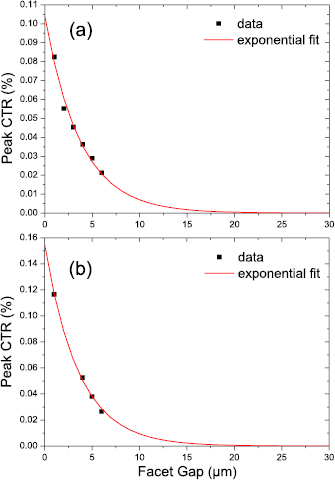
Figure 9. Measured data and exponential fit of the peak CTR-gap curves for the interconnects with 10 µm-wide (a) and 50 µm-wide (b) LEDs as a function of the coupling gap.
Download figure:
Standard image High-resolution imageThe role of the sidewall metal on the LED mesa is studied by comparing the interconnect performance with different sidewall coating designs. In addition to the LEDs discussed above with three sidewalls coated with Ti/Au metal, a 50 µm-wide LED with only 6.5% of the area of three sidewalls coated with metal (simply termed 'LED without sidewall metal' here) for the electrical connection to metal pads is also fabricated as shown in the inset of figure 10(a), and it is connected with a 60 µm-wide SU-8 waveguide and 70 µm-wide PD for a referential optical link. From the performance comparison shown in figure 10(a), the metal on the LED mesa sidewalls have little effect on the IPD–ILED response curve of the optical interconnect. To remove the effect of the height non-uniformity of different SU-8 waveguides, we also compare the results when the SU-8 waveguides are absent, which is shown in figure 10(b). Although the response currents are reduced by two orders of magnitude compared with figure 10(a), the LEDs with sidewall metal do not show any increase of response current over that without sidewall metal, which definitely indicates that reflecting the light from the other sidewalls does not enhance the light output from the front facet. This can be explained as that the in-plane LED light reflection from the flat interfaces of III–V/SiO2/air is already as high as that from the interfaces of III–V/SiO2/metal, and the light absorption by the sidewall metal is nearly as much as the light output from the sidewalls without metal. A finite-difference time-domain simulation of the light transmission at the flat III–V/SiO2/SU-8 interfaces shows that the collected light from an LED to SU-8 is limited to incident angles less than ±30° because of the total light reflection for larger incident angles by the flat interfaces. Therefore, the in-plane light reflection by the front facet of our LEDs should be reduced to enhance the light output, so as to increase the CTR of our optical interconnects. Because of the broadband light emission of the LEDs, it is challenging to achieve an adequate anti-reflective film coating. Alternatively, specific facet designs (such as jagged or convex facets) could be employed to increase the LED output, which has already been demonstrated in our preliminary experiments.
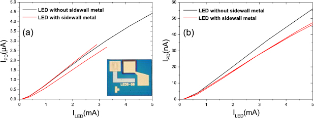
Figure 10. Response comparison between interconnects with LEDs with and without metal-coated sidewalls when the SU-8 waveguides are present (a) and absent (b). The inset in (a) shows the microscopic map of the LED mesa with only a small sidewall area coated with metal.
Download figure:
Standard image High-resolution imageThe commercial opto-isolators using GaAs LEDs and Si-based PDs or phototransistors are uni-directional since the photo receivers cannot emit light. Thus it is very useful to develop a bidirectional opto-isolator because it can replace two uni-directional opto-isolators symmetrically placed between two electrically isolated circuits for bidirectional data communication. Since our LEDs and PDs are based on the same epitaxy, it is feasible to achieve on-chip bidirectional opto-isolators with our design. Reverse-direction transmission of our optical interconnect is demonstrated with the 70 µm-wide PD acting as a light source and the 50 µm-wide LED acting as a detector, as revealed in figure 11(a). Compared with the forward-direction transmission results in figure 4(a), the reverse-direction one shows a wider linear operation range because the light source in the reverse-direction transmission has a larger current injection area than that in forward-direction one. The peak CTRs in the reverse-direction transmission are lower than those in the forward-direction one. This is partly because, in the reverse-direction transmission, the waveguide width (60 µm) is smaller than that (70 µm) of the light source and larger than that (50 µm) of the receiver, reducing the coupling efficiencies. Also, the small length of the receiver in the reverse-direction transmission reduces its responsivity, which can also be seen by the more obvious effect of the reverse bias on the CTR in figure 11(a) compared to that in figure 4(a). If we transform the I–I response curve to current density versus current (J–I) response curve, both the forward-direction and reverse-direction transmission show very similar response curves, as shown in figure 11(b). Therefore, reciprocal J–I transmission is demonstrated in our optical interconnect, which is beneficial for the realization of bidirectional opto-isolators.

Figure 11. (a) LED response and CTR as a function of PD current for reverse-direction interconnect. (b) Comparison of J–I response curves between the forward-direction and reverse-direction transmission.
Download figure:
Standard image High-resolution image
5. Conclusions
In conclusion, we have presented compact, low profile optical interconnects of micron sized LEDs coupled to micron sized PDs on silicon, realized for the first time using transfer-printing. Data transmission is demonstrated with very low power consumption and good SNR. The low LED output efficiencies are demonstrated to be the main limiting factor for the CTR or efficiency of our optical interconnects. The effects of the reverse PD bias, SU-8 waveguide and LED sidewall metal on the interconnect performance are studied. The interconnect loss can be reduced by improving the waveguide sidewall flatness and limiting the LED emission directions. The front facet design of the LEDs should be engineered to reduce the facet reflection so as to enhance the extracted power from the LEDs. The form factor of our optical interconnect can be further reduced by removing the probe pads from the printed devices and the devices would be electrically connected with the drive circuits on the silicon substrate, and the number of devices (LEDs and PDs) from a III–V wafer can also increase significantly. Furthermore, it is practical to make stand-alone micro-packaged optical links that can be integrated onto CMOS circuits with no additional lithography or metallization processes [34]. The advantages of the efficient light coupling, bidirectional optical interconnect, small form factor and easy heterogeneous integration of our interconnect over traditional free-space edge-coupled LED-to-PD interconnect make it very suitable for applications like on-chip opto-isolators. Our approach is very powerful for realizing different circuits on silicon or other platforms by heterogeneous integration. For example, it is applicable to realize high bandwidth on-chip optical links based on transfer-printed LDs butt-coupled to waveguides and PDs.
Acknowledgments
This work is supported by Science Foundation of Ireland through the Irish Photonic Integration Centre Award 12/RC/2276.