
Abstract
Detailed knowledge of the dopant concentration and composition of wide band gap AlxGa layers is of crucial importance for the fabrication of ultra violet light emitting diodes. This paper demonstrates the capabilities of wavelength dispersive x-ray (WDX) spectroscopy in accurately determining these parameters and compares the results with those from high resolution x-ray diffraction (HR-XRD) and secondary ion mass spectrometry (SIMS). WDX spectroscopy has been carried out on different silicon-doped wide bandgap AlxGa
 samples (x between 0.80 and 1). This study found a linear increase in the Si concentration with the SiH4/group-III ratio, measuring Si concentrations between
  cm−3 and
  cm−3, while no direct correlation between the AlN composition and the Si incorporation ratio was found. Comparison between the composition obtained by WDX and by HR-XRD showed very good agreement in the range investigated, while comparison of the donor concentration between WDX and SIMS found only partial agreement, which we attribute to a number of effects.
Export citation and abstract BibTeX RIS

Original content from this work may be used under the terms of the Creative Commons Attribution 3.0 licence. Any further distribution of this work must maintain attribution to the author(s) and the title of the work, journal citation and DOI.
1. Introduction
Wide bandgap group-III nitride semiconductors are of significant current interest due to the numerous possible applications of ultra violet (UV) light emitting devices, including: water purification [1], gas sensing, and medical diagnostics. High quality AlxGa N:Si layers are needed for the n-type layers in multi-quantum well based UV light emitting devices, but the growth of these still presents challenges. AlxGa
 layers with a high AlN content
  suffer from a nonlinear increase in the activation energy of the silicon donor from 12–17 meV in GaN [2] up to 238–255 meV in AlN [3, 4]. This is due to formation of donor bound excitons at the Si site as well as a reduction in the formation energy of compensating and self-compensating defects [5, 6] resulting in a reduced carrier density at room temperature. Furthermore, it is not yet understood to what extent the incorporation of the Si donor depends on the alloy composition, and no experimental observation of a possible Si solubility limit has been made.
As small variations in the composition as well as doping and impurity concentration can have a strong effect on the performance of a device, reliable methods for determining these variables are required to underpin the optimization of growth conditions and achieve high efficiency devices. In this paper we report on the determination of composition and doping concentration in wide band gap AlxGa N:Si layers using wavelength dispersive x-ray (WDX) spectroscopy in an electron probe microanalyzer (EPMA) and compare the results with: x-ray diffraction (XRD) and secondary ion mass spectrometry (SIMS).
XRD measurements are widely used to obtain compositional information of semiconductor structures. This is achieved by measuring the lattice constant of a given layer and requires prior knowledge of the strain state of the semiconductor in order to precisely determine the composition. Due to the negligible effect of impurity atoms and dopants on the lattice spacing, their concentration cannot be obtained by XRD. In order to quantify these, SIMS is usually used in tandem with XRD.
Using WDX-EPMA to measure the composition and dopant concentration offers some distinct advantages. Unlike SIMS, WDX is non-destructive and can readily be used for quantitative multi-element analysis, allowing determination of the composition and doping concentration at the same time. Furthermore the calibration standards used for WDX are less costly than the ion-implanted standards required for the calibration of SIMS measurements determining the dopant concentration. WDX also allows for correlation with other scanning electron microscope (SEM) based techniques like secondary/backscattered electron imaging, cathodoluminescence (CL), electron beam induced current, or electron back scattered diffraction (EBSD), measuring multiple intrinsic properties at the same time [7–10]. WDX furthermore enables one to perform qualitative and quantitative element maps, obtaining information about compositional variations on a lateral scale with submicron spatial resolution [11]. The capability to reliably determine the dopant concentration using WDX in group-III nitrides has been demonstrated by Deatcher et al [12] who measured Mg concentrations in GaN as low as  cm−3 with very good agreement between WDX and SIMS. The main disadvantages of using WDX instead of SIMS for the analysis of semiconductor materials are the higher detection limit and only a very limited ability to probe the atomic concentration as a function of depth. Additionally, the characterization of very thin films is challenging due to the requirement of a minimum electron energy to excite characteristic x-rays, depending on the elements under investigation.
2. Experimental
A number of samples have been characterized in order to determine the incorporation properties of the Si-donor in wide band gap AlxGa layers (see table 2). Each sample was grown by metalorganic vapor phase epitaxy (MOVPE) on a defect-reduced AlN/sapphire template [13] offering a threading dislocation density down to
  cm−2 [14]. The AlN composition of the samples characterized by WDX and XRD was varied from 80% to 100% and the SiH4/III ratio during growth between
  and
and  . The AlN composition of the very similar set of samples characterized by SIMS was varied from 50% to 100% and the SiH4/III ratio during growth between
  and
and  . TMAl, TMGa, NH3 and SiH4 were used as precursors. The thickness of the doped layers is between 1000 nm and 1600 nm, but the AlN is 3000 nm thick. More details on the growth of the AlxGa
 N:Si layers is given elsewhere [15].
All WDX measurements in the EPMA (Cameca SX100) were conducted with the incident electron beam normal to the sample surface, with an acceleration voltage of 10 kV and a beam current of 40 nA. At this acceleration voltage 90% of the beam energy is deposited in the first 600 nm of an AlN sample, according to Monte Carlo simulations using the CASINO software [16]. The beam energy is well above the minimum energy needed to excite the selected x-ray lines while containing the interaction volume within the desired layer, as for lower AlN% the penetration depth of the electron beam will be smaller due to the higher material density (e.g. for Al Ga
Ga 90% of the beam energy is deposited in the first 500 nm of the sample).
For the WDX characterization the peak-background signals were compared with those from AlN:Si and GaN standards to give the experimental k-ratios (sample intensity/standard intensity). The Ga and Al
 signals were recorded using a large TAP crystal (thallium acid phthalate,
  ) while for the NKα signal a synthetic pseudocrystal (PC1,
  ) was used. The measured k-ratios were converted to atomic percentages using correction routines on the EPMA.
In order to accurately determine the AlN content of AlxGa layers grown on top of AlN/sapphire templates by XRD, it is necessary to take the strain state in these layers into account. Therefore XRD reciprocal space maps (RSMs) near the asymmetric (10.5) reflection of AlN were recorded. Figure 1 shows the RSMs obtained for AlxGa
 layers with x = 0.80 (a) and x = 0.94 (b) grown on AlN. The diagonal lines in figure 1 indicate a strain-dependent movement of the reflection of a layer of fixed composition. The lattice constants in the basal plane (
 ) and in the growth direction (
 ) are determined from the peak position of the AlxGa
 reflection.

Figure 1. Reciprocal space maps near the asymmetric AlN (10.5) reflection of AlxGa layers with x = 0.80 ± 0.01 (a) and x = 0.94 ± 0.01 (b).
Download figure:
Standard image High-resolution imageUsing the condition for biaxial strained layers (equation (1)) and the definition of isotropic strain (equations (2) and (3)) Schuster et al derived equation (4) [17]. By applying Vegard's law to the a, and c lattice parameters as well as the elastic moduli C13 and C33 (see table 1) equation (4) can be solved analytically in order to determine the AlN mole fraction x corresponding to the measured  and
and  lattice parameters


Table 1. Material constants used for the XRD analysis [18–20].
a 
|
c 
|
C13 (GPa) | C33 (GPa) | |
|---|---|---|---|---|
| AlN | 3.112 ± 0.0005 | 4.982 ± 0.0005 | 98.9 ± 3.5 | 388.5 ± 10 |
| GaN | 3.189 ± 0.0005 | 5.185 ± 0.0005 | 106.0 ± 20.0 | 398.0 ± 20 |
Table 2. Overview of the analyzed samples, values are rounded to the last significant figure.
| Nr. | SiH4/III ratio (10−5) | AlN% XRD | AlN% WDX | Si WDX (1018 cm−3) | Si SIMS (1018 cm−3) |
|---|---|---|---|---|---|
| 1 | 1.92 | 82.3 ± 1.0 | 82.2 ± 2.5 | 4.2 ± 0.4 | |
| 2 | 5.94 | 80.3 ± 1.0 | 80.1 ± 2.5 | 14 ± 2 | 7.0 ± 3.5 |
| 2 | 4.1 ± 0.8 | ||||
| 3 | 17.7 | 82.7 ± 1.0 | 82.6 ± 2.5 | 28 ± 1 | |
| 4 | 4.16 | 86.8 ± 1.0 | 86.2 ± 2.6 | 6.3 ± 0.6 | |
| 5 | 6.00 | 84.7 ± 1.0 | 83.8 ± 2.6 | 9.0 ± 0.7 | |
| 6 | 7.06 | 84.2 ± 1.0 | 84.9 ± 2.6 | 11 ± 1 | |
| 7 | 10.1 | 85.1 ± 1.0 | 85.3 ± 2.6 |

|
|
| 8 | 14.8 | 86.3 ± 1.0 | 86.3 ± 2.6 | 25 ± 1 | |
| 9 | 0.972 | 95.9 ± 1.0 | 95.7 ± 2.9 | 3.0 ± 0.4 | |
| 10 | 2.14 | 93.7 ± 1.0 | 94.1 ± 2.8 | 5.7 ± 0.5 | |
| 11 | 3.50 | 94.7 ± 1.0 | 93.8 ± 2.9 | 7.0 ± 0.5 | 3.6 ± 0.7 |
| 12 | 4.50 | 94.7 ± 1.0 | 94.5 ± 2.9 | 9.3 ± 0.7 | |
| 13 | 5.50 | 95.6 ± 1.0 | 94.8 ± 2.9 |

|
|
| 14 | 6.62 | 94.7 ± 1.0 | 94.7 ± 2.9 |

|
|
| 15 | 1.99 | 87.1 ± 1.0 | 87.2 ± 2.6 | 5.4 ± 0.6 | |
| 16 | 2.06 | 88.3 ± 1.0 | 91.7 ± 2.8 | 5.0 ± 0.4 | |
| 17 | 2.14 | 94.4 ± 1.0 | 94.8 ± 2.9 | 5.4 ± 0.5 | |
| 18 | 8.09 | 100 ± 1.0 | 99.9 ± 3.0 | 3.0 ± 0.5 | |
| 19 | 00.0 ± 1.0 | 00.0 ± 0.0 | |||
| 20 | 28.5 | 100 ± 1.0 | 20 ± 10 | ||
| 21 | 5.91 | 80.0 ± 1.0 |

|
||
| 22 | 5.91 | 80.0 ± 1.0 |

|
||
| 23 | 2.34 | 50.0 ± 1.0 |

|
||
| 24 | 6.35 | 100 ± 1.0 | 1.0 ± 0.5 | ||
| 25 | 5.11 | 80.0 ± 1.0 | 4.1 ± 0.8 | ||
| 26 | 5.85 | 90.0 ± 1.0 | 4.7 ± 0.9 | ||
| 27 | 5.11 | 80.0 ± 1.0 | 3.8 ± 0.8 | ||
| 28 | 5.85 | 90.0 ± 1.0 |

|
The measurement error due to a tilt of the sample in the XRD sample holder was corrected by determining the tilt from a (00.2) omega scan after aligning the goniometer for the (10.5) reflex and correcting the measured RSM by the measured tilt value. The error was calculated using the sum of the weighted derivations of the tabulated material constants, as given in table 1 [18–20] as well as the measured lattice parameters ( ). An absolute error of ±1% in AlN fraction was obtained for all samples.
For the WDX characterization of the Si-dopant concentration in the different sample series, a pure Si wafer was used as a standard to determine the k-ratios with a large TAP crystal used to acquire the Si (K ) signal. The detector counting time was doubled compared to the counting times for Ga and Al due to the lower Si concentration. Each of the plotted WDX measurement points consists of the mean of 10 measurements performed along a line on each of the samples. The WDX errors shown consist of the standard error and an estimated systematic error of 3% of the measured signal (to account for matrix effects, difference between standards and samples, surface contamination, etc.) which is above the deviation from the weight total which was at
  for each investigated sample.
The Si concentration was also measured by SIMS, which (like WDX) is insensitive to either the elements site in the crystal lattice or to lattice distortions. During SIMS of high band gap AlxGa two effects influence the measurement. Firstly, matrix effects [21, 22] have an important effect on the relative ion yield as only a few percent of the sputtered species are ionized. Therefore, a range of reference samples with different AlxGa
 composition were used with different sputtering ions to determine the relative sensitivity factors (RSF) and the sputter rate. Secondly the accumulation of surface charges due to ion bombardment can strongly influence the secondary ion yield [23]. This was partially mitigated by deposition of a conductive metal layer and electron beam irradiation. The Si concentration was determined by the point-by-point correction protocol. The RSF are adjusted at each data point based on the AlxGa
 composition.
The SIMS detection limit, i.e. the lowest concentration measured of an element for a given set of analysis conditions, depends strongly on the AlN concentration. For example, in GaN the Si detection limit is  atoms cm–3 compared with
  atoms cm–3 in AlN. In Al
 Ga
Ga the detection limit for Si is
  atoms cm–3–
 atoms cm–3. The errors of the SIMS measurements were estimated by the companies who executed the measurements as 20% and 50% respectively, largely due to errors introduced by sample charging and possible matrix effects.
3. Results and discussion
3.1. Comparison of Al composition as determined by WDX and XRD
In figure 2 the AlN content determined by WDX is plotted versus the AlN content determined by XRD (10.5) RSMs of all samples. Neglecting the one sample at a XRD aluminum nitride content of x = 0.88 (WDX x = 0.92), there is very good agreement between all of the WDX- and XRD-determined AlN compositions. In addition to the Si-doped AlxGa samples, a GaN sample was investigated (see table 2). The WDX technique enables a non-destructive determination of the composition of wide bandgap AlxGa
 alloys and is in good agreement with XRD measurements, well below the margin of error (2.5%–3% AlN%, see table 2). Note that one can also quantify the composition of quaternary InAlGaN alloys using WDX, as demonstrated by Bejtka et al [24], which present further difficulties for XRD measurements due to the uncertainty of uniquely attributing lattice constants to compositions and strain.

Figure 2. AlN content of samples determined by WDX plotted versus the AlN content determined by XRD (10.5) RSMs.
Download figure:
Standard image High-resolution image3.2. Determination of the doping concentration by WDX
Figure 3 shows the Si concentration as determined by WDX measurements on all investigated samples (see table 2) and how this depends on their AlN concentration as well as the SiH4/III ratio. As indicated by the horizontal lines, this result shows that the Si incorporation of the investigated samples is independent of the composition of the sample and only depends on the SiH4/III ratio that was used during the growth. Junxue et al [25] proposed an increasing Si incorporation with increasing Al content, which they attributed to an increasing rate of parasitic prereactions in the gas phase with increasing TMAl partial pressure. However, as the TMAl partial pressure was kept constant for the samples in the present study and the variation of the composition was achieved by varying TMGa partial pressure, a negligible change in the amount of gas phase prereactions is expected, leading to a Si incorporation independent of the Al composition.
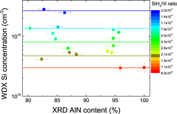
Figure 3. The dependence of the Si concentration measured by WDX on the AlN content and the SiH4/III ratio.
Download figure:
Standard image High-resolution imageIn figure 4 the measured Si concentration (log scale) is plotted against the SiH4/III ratio for all investigated samples. The WDX was fitted to a linear function with a gradient of  cm−3 and an intercept with the concentration axis of
  cm−3. The very good fit of the measurement data to a linear function shows that the Si incorporation in wide band gap AlxGa
 layers increases linearly with the SiH4/group-III ratio. This is in good agreement with findings by other groups [26–28]. For the range of SiH4/group-III ratios under investigation no saturation could be observed.
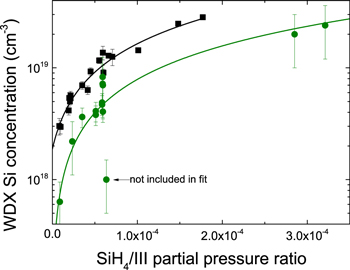
Figure 4. Log-linear plot of the Si concentrations determined by WDX (black squares) as well as SIMS (green circles) versus the SiH4/III ratio. Linear fits of the data are shown as lines.
Download figure:
Standard image High-resolution imageComparing the WDX results for the Si concentration with commercially performed SIMS results (see figure 4) we found that both measurement methods show the same general trend: a linear increase in the Si concentration with increasing SiH4/III ratio. Comparing the Si concentration values we find only partial agreement in the absolute concentration values between the two measurement methods. The linear fits of the two series show that the measured Si concentration differs by a factor of approximately 2. For example for an Al Ga
Ga layer with a SiH4/III ratio of
  the Si concentration was determined to be
  cm−3 by SIMS, whereas the Si concentration determined by WDX is
  cm−3. For an Al
 Ga
Ga layer with a SiH4/III ratio of
  the discrepancy increases even further, for the measurements done by the same company, giving Si concentrations of
  cm−3 and
  cm−3 for WDX and SIMS, respectively. The SIMS measurements carried out by another employed company on the same sample yielded a Si concentration of
  cm−3 demonstrating that the values obtained by SIMS are very sensitive to the measurement setup and calibration standard.
The disagreement between the two measurement methods (and the two SIMS measurements) could be caused by a variety of effects including the matrix effect and sample charging. The matrix effect is a well known problem for SIMS measurements, changing the secondary ion yield depending on the matrix (i.e. composition of the sample) the ions are embedded in. To compensate for this SIMS standards with a known composition close to the investigated samples are needed. Standards fulfilling this criteria were utilized in these measurements reducing the possible influence of the matrix effect. The same effect can also influence WDX measurements [29]. To reduce the influence of the matrix effect on the measured Si concentration a software correction was applied. It has to be noted that in previous measurements of Mg in GaN very good agreement between WDX and SIMS was found [12]. The difference between the SIMS measurements of both companies might stem from the use of different standards for the Si determination.
Sample charging provides another challenge to overcome in acquiring precise concentration measurements utilizing charged particles for the group-III nitride system, and this proves especially challenging in undoped AlxGa layers with high AlN concentrations. Although the investigated samples are all Si doped, charging effects were still observed, influencing the measured concentrations. An estimate of the charging on the WDX measurements can be gained by analyzing the weight total, where a deviation from the optimum value (100%) can indicate that the obtained data has been influenced by effects like sample charging. In this sample series all WDX measurements resulted in a weight total of
  , with no dependence on composition, indicating that sample charging had a negligible effect on the WDX measurement. SIMS measurements are expected to show a stronger dependence on sample charging effects than WDX as both the primary as well as the secondary ions will be affected by a build-up in surface charge. To reduce the effect of sample charging, Au coating and electron bombardment were used for the SIMS measurements. However, even with the discrepancy of a factor of 2 between SIMS and WDX measurements (and no clear indication which technique is right) WDX provides accurate measurements with small errors and is capable in measuring impurity concentrations as low as 3 × 1018 cm−3.
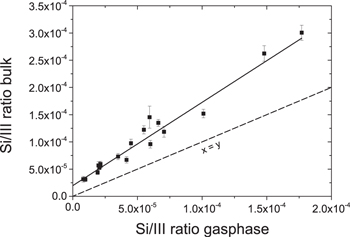
In figure 5 the Si/III ratio in the bulk is plotted against the SiH4/III ratio in the gas-phase. The Si incorporation increases as expected linearly with the SiH4/III ratio, with a gradient of 1.45, showing that no saturation of the Si incorporation can be observed in the investigated range. As the Si incorporation on group-III lattice sites is strongly preferred over the incorporation on a N site, one can conclude that the incorporation of Si atoms is slightly preferred over the incorporation of group-III atoms [30, 31]. This is most likely a result of pre-reactions in the gas-phase which reduce the amount of available Ga and Al atoms for incorporation [32]. Additionally desorption of Ga adatoms from the surface could further decrease the amount of III-atoms. All parameters as determined by WDX, XRD, and SIMS are summarized in table 2.
Figure 5. Comparison between SiH4/III ratio in gas-phase and bulk: the solid line is a linear fit over all data points, while the dotted line shows equal Si/group-III ratio in gas-phase and bulk.
Download figure:
Standard image High-resolution image
4. Summary
We have successfully demonstrated the use of WDX spectroscopy in a commercially available EPMA for the characterization of Si doped wide bandgap AlxGa layers, determining the Si concentration as well as the composition of the investigated layers. Very good agreement in the determination of the composition was found between WDX and XRD, while comparison between SIMS and WDX measurements of the Si concentration showed only partial agreement which has been attributed to possible charging effects during the SIMS measurements and matrix effects influencing both SIMS and WDX characterization.
It was found that the Si concentration increases linearly with the SiH4/III ratio, and no solubility limit of Si in AlxGa could be found within the measurement range investigated (up to
  cm−3).
The ability of WDX to determine the composition as well as the Si doping concentration, in the concentration regime important for the fabrication of devices (demonstrated in the range of  cm−3
cm−3  cm−3), offers distinct advantages over XRD and SIMS measurements which can only reliably provide the information on one of these parameters. Furthermore, WDX allows the correlation with other SEM-based techniques such as cathodoluminescence and electron channelling contrast imaging, possibly providing information about interactions between threading dislocations, luminescence properties, and compositional or doping concentration variations.
Acknowledgments
We are grateful to Dr Stuart Kearns of Bristol University for insightful advice regarding the WDX analysis. The authors would like to thank Dr Arne Knauer and Dr Viola Kueller (Ferdinand-Braun-Institut, Leibniz-Institut für Höchstfrequenztechnik) for providing ELO AlN/sapphire templates. We acknowledge funding from the Engineering and Physical Sciences Research Council (EPSRC) (EP/M003132/1) of the UK. The data associated with this research is available at doi: 10.15129/fe2ea4ed-235c-4f7e-9301-4c9677bffddb. The research was partially supported by the Deutsche Forschungsgemeinschaft (DFG) within the collaborative Research Center 'Semiconductor Nanophotonics' (SFB 787) and the German Federal Ministry of Education and Research (BMBF) within the ʻUltraSens' project under contract number 13N12587 and 'Advanced UV for Life' under contract numbers 03ZZ0105B, 13N12587 and 03ZZ0103.