

Abstract
In this work we report on the performance of mid-infrared quantum cascade lasers (QCLs) based on strained InGaAs/AlGaAs grown by molecular beam epitaxy on GaAs substrate. Structures were grown with indium content from 1% to 6% in GaAs quantum wells (QW) and 45% of Al in AlGaAs barrier layers. The design results in strained heterostructure, however, no strain relaxation was observed as documented by x-ray diffraction measurements up to ∼3% of In content in QWs. The investigation of heterostructures and devices was performed, including structural measurements and electrooptical characterization of devices. Devices fabricated from epi wafers with 2.64% of In exhibited performance largely improved over GaAs/AlGaAs QCLs. Roughly two times reduction of the threshold current density was observed at lasing wavelength ∼9.45 μm. The lasers operated in pulsed mode up to T = 50 °C with characteristic temperature T0 = 115 K. The decrease of the threshold current density has been mainly attributed to the reduction of interface roughness scattering and the increase of activation energy for the escape of carriers from the upper laser level to the 3D continuum. Further increase of In content in QWs resulted in the deterioration of device parameters.
Export citation and abstract BibTeX RIS
1. Introduction
MID-IR GaAs-based quantum cascade lasers (QCLs) can be divided into two main categories based on the material system involved, i.e. GaAs- and InP-based devices. The latter offer unquestionable advantages in terms of high temperature, CW operation whereas the former operate at room temperature only in pulsed mode. However, because the cost and complexity of technology and fabrication is much lower for GaAs based devices they still might be of interest for less demanding applications. The main issue that limits high temperature performance of GaAs-based devices is low conduction band-offset, causing the electrons to escape to 3D continuum of states at elevated temperatures of active region. In this work, we attempt to overcome this limitation and improve the high temperature performance of the devices.
The first GaAs based QCLs have utilized Al content of 33% in AlGaAs barrier layers [1]. With low-loss Al-free waveguide the threshold current density of 5.0 kA cm−2 at 77 K and a maximum pulsed operation temperature of 200 K has been achieved [2]. The relatively large threshold current density Jth and power consumption of AlGaAs/GaAs QCL have made it very challenging to achieve room temperature operation. The progress in device performance has been made by increasing Al content in the barriers to 45%. Room temperature pulsed operation has been reported for three quantum-well active region design [3], superlattice active region design [4] and bound-to-continuum active region design [5]. The optimized device processing resulted in CW operation in temperatures up to 150 K [6]. There were also attempts taken to increase the band offset by e.g. increasing the Al content in the barrier layers beyond the 45% [7, 8]. In the first case, AlAs barriers were used which resulted in ∼1 eV conduction band discontinuity [7]. However, despite decreasing thermally activated carrier escape and achieving very high T0 equal to 320 K the maximum operating temperature was only 230 K, being limited by negative differential resistance effects that occurred with increasing applied bias. Another approach was based on modifying the aluminum composition, and hence the height, of a single barrier in each active region [8]. Also in this case, despite improving threshold current density at low temperatures (3.8 kA cm−2 at 11 K) the maximum operating temperature was only slightly above 150 K, which indicated that the confinement of the upper laser level is not the dominant factor affecting the temperature performance of this laser design. Poor performance of the lasers with high Al content in the barriers has been attributed to increased inter-valley scattering to X minimum [9, 10], which led to abandoning this type of design.
An alternative approach to increase band-offset is to deepen GaAs quantum wells (QW) by using InGaAs alloy. This has been done by introducing 4% of In into QWs in the active region [11]. No In was added to the injectors in order to keep the overall strain at low level. However, the results were not very encouraging, the maximal working temperature of only 200 K has been achieved which was interpreted as being the result of the misalignment of the injector with the upper laser level at elevated temperatures and increasing carrier leakage. In another approach InAs monolayers were deposited in the device active region and AlAs barriers were used, which allowed for room temperature operation (up to 305 K with Jth ∼25 kA cm−2) [12].
In this paper, we present GaAs-based QCLs characterized by improved high temperature operation. This has been achieved by adding small fraction (up to 3% by design) of In to all QWs in the active core, resulting in a strained InGaAs/AlGaAs heterostructure design. The preliminary results of this work have been reported in [13]. The characteristics of modified devices will be compared to the ones of GaAs/AlGaAs devices, grown and fabricated at the Institute of Electron Technology.
In our previous works on GaAs-based QCLs [14–16] we have demonstrated GaAs/AlGaAs lasers operating at 300 K in pulse mode, and showing high peak power output at cryogenic temperatures [14]. The peak powers recorded in 77 K were over 4 W (25–35 mW at 300 K), and the slope efficiency was equal η ≈ 0.5–0.6 W A−1 per uncoated facet (η ≈ 1 W A−1 for lasers with metallic back mirror coating). These results are comparable with the state-of-the-art GaAs/AlGaAs devices of similar design produced in other laboratories [17, 18].
2. Experimental results
The investigated InxGa1−xAs/Al0.45Ga0.55As QCL laser structures are compared to reference GaAs/Al0.45Ga0.55As QCL lasers crystalized in the same growth campaign at the same growth conditions, with the same thickness of individual layers and the same doping. The results presented in this paper are based on the total number of 9 epitaxial runs for GaAs/AlGaAs and 16 runs for InGaAs/AlGaAs lasers with In content ranging from ∼1% to ∼6%, performed over the two year period.
A detailed investigation of structural properties of heterostructures, as well as thorough device characterization has been performed, to provide meaningful conclusions about the origin of observed performance improvement. Several experimental techniques have been used in this study, including x-ray measurements, transmission electron microscopy and electrical characterization (light–current–voltage curves). Finally, advanced device modelling was performed to support the conclusions of experimental works.
2.1. Investigated samples
Here, we report on the design, fabrication and characterization of QCLs based on strained InGaAs/AlGaAs heterostructure. Contrary to the previous reports where In has been added to the active wells only we add small amount of In to both active QWs and the injectors. The conduction band profile and moduli squared wavefunctions in injector/active/injector segment of the In0.03Ga0.97As/Al0.45Ga0.55As laser under the applied field of 48 kV cm−1 at 300 K are shown in figure 1.

Figure 1. Conduction band profile and moduli squared wavefunctions in injector/active/injector segment of the In0.03Ga0.97As/Al0.45Ga0.55As laser under an applied field F = 48.0 kV cm−1 at 300 K. The E3, E2 and E1 refer to the upper, lower and ground state of lasing transitions. The lowest energy state in the injector couples directly to the upper laser level E3. 3D denotes first of the continuum-like states existing above barriers.
Download figure:
Standard image High-resolution imageThe levels E3, E2 and E1 refer to the upper, lower and ground state of lasing transitions. For strained In0.03Ga0.97As wells we get ∼30 meV larger band offset comparing to pure GaAs [19]. The activation energy for the escape to 3D continuum is higher in strained design comparing to GaAs/AlGaAs design. For strained design, 3D-E3 distance, equals to ∼105 meV, whereas in case of GaAs/AlGaAs QCL it is ∼80 meV.
The laser structure consists of the 36-period sequence of injector +3QW segments. The active region was based upon the three QW design [14]. The layer sequence of one period of the structure, from left to right, starting from the injection barrier is: 4.6, 1.9, 1.1, 5.4, 1.1, 4.8, 2.8, 3.4, 1.7, 3.0, 1.8, 2.8, 2.0, 3.0, 2.6, 3.0 nm. AlGaAs barrier layers are denoted in bold, InGaAs wells are denoted in normal font. The total thickness of one period is 45.0 nm. The underlined layers are n doped to 6 × 1017 cm−3. The structures used a double-plasmon Al-free waveguide for planar optical confinement.
The laser structures were grown by solid source molecular beam epitaxy (MBE). The growth of GaAs layers was performed from two Ga effusion cells simultaneously, whereas AlGaAs layers were grown from one Ga and one Al cell which ensured similar growth rate (∼0.19 nm s−1). The In influence on the growth rate can be neglected. The active core and the waveguide layers were grown at the same growth rate. The As2 flux was set at 5.6 × 10⁻⁶–5.8 × 10⁻⁶ in all cases. The waveguide layers were grown at 580 °C. The active core layers of InGaAs/AlGaAs QCL's were grown at 520 °C whereas that of GaAs/AlGaAs QCL's at 580 °C. The details of layer structure of the laser are listed in the table 1.
Table 1. The layer structure of InxGa1−xAs/Al0.45Ga0.55As QCLs.
| Thickness | Material | Doping | |
|---|---|---|---|
| 1.0 μm | GaAs | n = 6 × 1018 cm−3 | Contact layer |
| 3.50 μm | GaAs | n = 4 × 1016 cm−3 | Upper waveguide |
| 1.620 μm | InGaAs/AlGaAs or GaAs/AlGaAs | Active region | |
| 3.50 μm | GaAs | n = 4 × 1016 cm−3 | Lower waveguide |
| 1.00 μm | GaAs | n = 6 × 1018 cm−3 | |
| 4500 μm | GaAs | n = 3 × 1018 cm−3 | Substrate |
Epitaxial wafers were processed into double trench mesa lasers with Si3N4 isolation layer. Details of the processing technology are given in our earlier papers concerning GaAs based QCLs [14–16, 20]. Devices with 15 and 25 μm width and 2 and 3 mm long cavities were fabricated. The lasers were mounted epi-side down onto a copper submount using indium solder. Only as cleaved, uncoated devices were investigated.
2.2. Structural characterization
A combination of high-resolution x-ray diffraction and scanning transmission electron microscopy (STEM) was used to determine alloy composition, layer thickness and interfaces quality. The epitaxial structure characterization was performed using PANalytical X'Pert PRO diffractometer. The details of the experiment can be found in [21]. The reflection intensity was measured by two counters; proportional detector and PIXcel—second generation solid state detector for counting photons with a high spatial resolution and high dynamic range.
The 2θ/ω scans for symmetric reflection 004 in triple axis geometry were measured. 2θ/ω scans yield information about lattice distortion in selected reciprocal space direction. Theoretical x-ray diffraction profiles were calculated utilizing dynamical diffraction theory.
The experimental 2θ/ω curves of the (004) reflection for GaAs/AlGaAs and nominally containing 3% of indium, InGaAs/AlGaAs QCL structure are presented in figure 2(a). The highest intensity peaks observed are GaAs substrate peak S and 0th order satellite peak (SL), related to the average lattice constant of the superlattice. The number of higher-order SL are also recorded. The thickness of the period calculated from the separation of SL peaks was equal to 45.0 nm and 44.8 nm for GaAs/AlGaAs and InGaAs/AlGaAs structures, respectively. The angular position of the 0th peak is generally sensitive to the composition of the constituent layers as well as to the strain present in individual layers. The exact content of aluminum (Al) for GaAs/AlxGa1−xAs structure and aluminum (Al) and indium (In) for InyGa1−yAs/AlxGa1−xAs was obtained from 0th peak position. The x value in AlxGa1−xAs layers for the both structures was 45% while the exact value in InyGa1−yAs layers for the InGaAs/AlGaAs QCL has been found to be equal 2.64%. This relatively small indium content in the QWs of InGaAs/AlGaAs structure affects the angular position of 0th peak because in introduces the additional strain in the structure. Therefore, the change of the perpendicular lattice mismatch (Δa/a)⊥ between these two structures is observed; figure 2(b). The perpendicular lattice mismatch was calculated using formula:
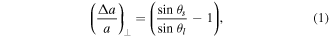
where: θs—angular position of GaAs substrate 004 reflection peak, θl—angular position of the 0th diffraction peak for (004) symmetrical reflection of the superlattice. The values of the (Δa/a)⊥ are 490 ppm for GaAs/AlGaAs structure and 2680 ppm for InGaAs/AlGaAs structure. As can be seen the strain in the InGaAs/AlGaAs structure is roughly five times greater than in the GaAs/AlGaAs structure. However, the crystalline quality of the InGaAs/AlGaAs structure still did not deteriorate. The intensive and narrow higher order SL are observed, figure 2(c). The SL are generally narrow. Their residual broadening reflects the influence of interface roughness and small fluctuations of period thickness with those two difficult to separate [21].
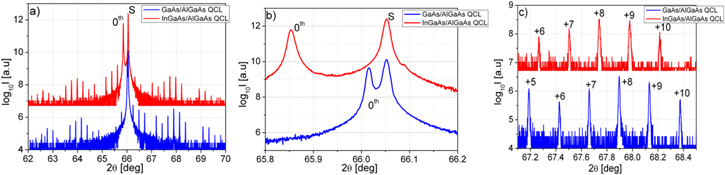
Figure 2. (a) (004) high-resolution diffraction scans of GaAs/AlGaAs and InGaAs/AlGaAs QCL structures. (b) Detailed view of GaAs substrate peak S and 0th order satellite peak. (c) The enlarged area around higher order satellite peaks.
Download figure:
Standard image High-resolution imageThe crystal quality and relaxation process in InGaAs/AlGaAs QCL structures was determined by measurements of the reciprocal space maps for symmetrical (004) and asymmetrical (−2–24) GaAs Bragg reflections along the [110] direction (see figure 3). A very small diffuse scattering is observed but it does not affect the high crystal quality of this structure. The asymmetrical space map shows no shift between GaAs and superlattice SL0A peaks in Qx direction indicating lack of relaxation. The onset of strain relaxation has been studied in a separate paper [22]. Here we summarize the results for the perpendicular lattice mismatch (Δa/a) and In content in InGaAs/AlGaAs QCL structures. The experimental (Δa/a) values determined from the difference between the angular positions of SL0 and GaAs peaks are shown in figure 4. For In content up to ∼3% the parallel lattice constants of the substrate and SL are the same, i.e., no relaxation occurred, however, a small asymmetrical diffuse scattering was observed for but it did not affect a high crystal quality of these structures. For In content above ∼3% we observe partial relaxation of the structure.
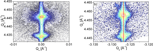
Figure 3. The reciprocal space maps along [110] direction for structure with 2.6% In content around symmetrical (004) (a) and asymmetrical (−2–24). (b) GaAs reciprocal lattice point. The red line indicates the case when the parallel lattice constants of superlattice SL0 and substrate GaAs are equal.
Download figure:
Standard image High-resolution image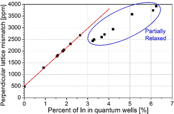
Figure 4. The perpendicular lattice mismatch as a function of In content in InGaAs/AlGaAs QCL structures.
Download figure:
Standard image High-resolution image2.3. Scanning transmission electron microscopy (STEM)
Both types of the QCL structures, i.e. InGaAs/AlGaAs and GaAs/AlGaAs were investigated by STEM (Hitachi HD-2700, 200 kV, cs-corrected). This 200 kV, field emission STEM machine equipped with bright-field (BF) and high-angle annular dark-field (HAADF) detectors situated below specimen position collect electrons transmitted through the specimen. The STEM observations allow us to obtain images providing complimentary information for the same area where BF STEM image is coupled with diffraction contrast and HAADF STEM image reveals Z-contrast coming from the atomic number. For the HD-2700 microscope equipped with a cs corrector and an Schottky-field-electron emitter an electron probe of 1.2 Å diameter can be formed.
HAADF STEM images do not show contrast reversal against thickness and defocus unlike high-resolution transmission electron microscopy images. Thereby bright spots, on images gained at atomic resolution, can be considered as projected atomic columns except for some defocus conditions [23]. In conventional TEM observations of similar heterostructures contrast delocalization occurs. The contrast of STEM images is less sensitive to local sample variations; it has been experimentally confirmed that no contrast reversal occurs in STEM for a wide range of focus and foil thickness. Furthermore, the STEM allows high-resolution images to be taken from thicker foils to minimize surface relaxation. Additionally, Z-contrast STEM images add another dimension for mapping lattice chemistry distribution at the same time.
High-resolution microscopy offers possibility of locally determining the microstructure of crystalline objects on an atomic scale. Studies of atomic defects as well as structural or chemical changes within one or two atomic positions require very thin, crystalline specimens. The preparation of TEM lamellae of studied structures is problematic. During ion milling segregation of In occurs and the etching speed is differentiated between the substrate and sample layers. The thin foils for STEM observations were prepared using a Focused Ion Beam technique (FIB/SEM integrated system Hitachi NB5000). To minimize damages occurred during the lamellae preparation the ion-beam energy during thinning process was progressively lowered down to 2 kV at the final stage. FIB processing guarantees uniform thickness at the whole area of TEM lamella. High-resolution observations were used to study the interface roughness.
Figure 5 shows a typical cross-section HAADF STEM images of a part of an active region of GaAs/AlGaAs laser where AlGaAs barriers have dark contrast and GaAs wells have bright contrast, which is connected with their average atomic number. Figure 6 presents typical HAADF STEM images of a part of active region of InGaAs/AlGaAs laser, with AlGaAs barriers having dark contrast and InGaAs wells having bright contrast.

Figure 5. Cross-section HAADF STEM images of part of GaAs/AlGaAs laser active core.
Download figure:
Standard image High-resolution image
Figure 6. Cross-section HAADF STEM images of part of In0.026Ga0.974As/AlGaAs laser active core.
Download figure:
Standard image High-resolution imageBoth heterostructures show very good quality of growth, with well defined QW and barrier layers. The differences between investigated structures are visible at higher magnification. The interfaces for the GaAs/AlGaAs system are not so smooth and some roughness (islands) is visible (figures 5 and 7), whereas the InGaAs/AlGaAs system shows smooth interfaces (figure 6).
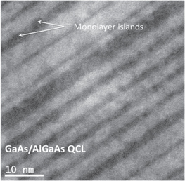
Figure 7. Cross-section high-resolution HAADF STEM images of the interfaces in GaAs/AlGaAs laser active core.
Download figure:
Standard image High-resolution imageIn order to quantify sharpness of interfaces of both structures we derive the distribution of the gallium, aluminum and indium atoms across interfaces by using averaged line profiles (see figure 8). The intensity profiles performed at the acquired images across a few interfaces show that GaAs/AlGaAs structure has more diffusive character, whereas for In0.026Ga0.974As/AlGaAs structure sharp transition between individual layers is observed confirming STEM observations. The results of structural characterization demonstrate that introducing In to the GaAs/AlGaAs structure can improve the interface roughness because In as a surfactant can enhance the surface migration of Al ad atoms during MBE This observation is in good agreement with data presented in the literature [24–26].

Figure 8. Intensity profiles performed at the acquired images of GaAs/AlGaAs and In0.026Ga0.974As/AlGaAs structures across a few interfaces.
Download figure:
Standard image High-resolution image3. Device characterization
For electrical characterization in pulsed operation mode we use typical set-up for QCL light–current–voltage characteristics (LIV) measurement [27]. Current pulses of 200 ns width and low duty cycles (0.1%) are used in order to avoid laser heating. The average output power is measured using TE-cooled VIGO MCT detector placed in front of the laser facet with AR-coated optics to improve light collection efficiency.
For temperature dependent measurements, QCLs were placed into liquid nitrogen cryostat, allowing LIV measurements in the temperature range from 77 K up to room temperature (300 K) or on the temperature-stabilized heat sink with a water-cooled Peltier element, allowing LIV measurements in the temperature range from 10 °C up to 90 °C. LIV characteristics for an In0.026Ga0.974As/AlGaAs QCL are shown in figures 9 and 10, whereas figure 11 shows corresponding characteristics of GaAs/AlGaAs QCL.
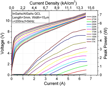
Figure 9. LIV characteristics of In0.026Ga0.974As/AlGaAs QCL. The data were collected in temperature range from 77 K to RT (293 K). Lasers with uncoated facets were investigated.
Download figure:
Standard image High-resolution image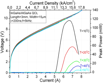
Figure 10. LIV characteristics of In0.026Ga0.974As/AlGaAs QCL in temperature range from 10 °C up to 50 °C. Lasers with uncoated facets were investigated.
Download figure:
Standard image High-resolution image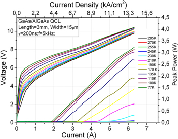
Figure 11. LIV characteristics of reference GaAs/AlGaAs. The data are collected in temperature range from 77 to 285 K. Lasers with uncoated facets were investigated.
Download figure:
Standard image High-resolution imageLIV characteristics for In0.026Ga0.974As/AlGaAs QCL and reference GaAs/AlGaAs QCL are compared in figure 12(a) for temperature of 77 K and in figure 12(b) for 250 K. The latter was chosen such so the GaAs/AlGaAs QCL would still emit some radiation.
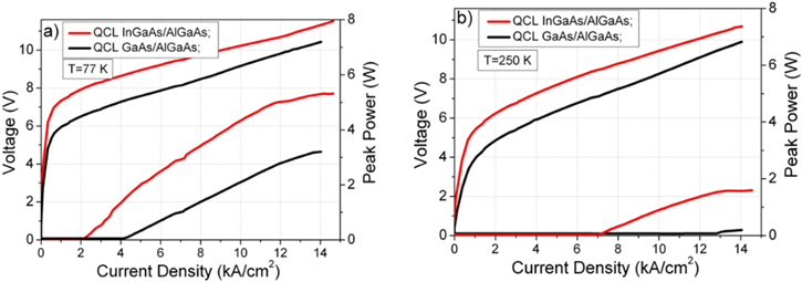
Figure 12. Light–current and current–voltage characteristics registered for GaAs/AlGaAs QCL (black lines) and for In0.026Ga0.974As/AlGaAs QCL (red lines) at T = 77 K (a) and at T = 250 K (b). Lasers with uncoated facets were investigated.
Download figure:
Standard image High-resolution imageThe In containing QCLs outperform standard GaAs/AlGaAs lasers. The advantage is gained in terms of threshold current and maximum operating temperature. At 77 K, the threshold current density for InGaAs/AlGaAs QCL is ∼1.9 times lower than the one for GaAs/AlGaAs laser, at 250 K threshold current reduction is ∼1.8. The values of 2.2 kA cm−2 at 77 K and 7.3 kA cm−2 at 250 K are the lowest threshold current densities ever obtained for GaAs based QCLs emitting in ∼9.x μm range. The emitted power is also considerably higher in the case of InGaAs/AlGaAs QCL, especially at elevated temperatures. At 77 K for 5 A (11.1 kA cm−2) of supply current strained InGaAs/AlGaAs QCL emits 2.4 times more power than GaAs/AlGaAs QCL. At 250 K for the same supply current strained InGaAs/AlGaAs QCL emits the maximal peak power (∼1 W), whereas GaAs QCL is still below the threshold.
The temperature dependent LIV characteristics enable us to determine the threshold current and the slope efficiency characteristic temperatures, T0 and T1, respectively. These quantities parameterize the increase (decrease) of the threshold current (differential slope efficiency) with increased temperature. Within a temperature range ΔT = Tmax − Tmin, these temperature dependencies can be written as:
Figure 13 shows threshold current density data versus temperature for In0.026Ga0.974As/AlGaAs QCL and GaAs/AlGaAs QCL. The value of T0 for In0.026Ga0.974As/AlGaAs QCL, extracted from the data for the whole temperature range 77–323 K equals 115 K, whereas for reference GaAs/AlGaAs QCL T0 =90 K, which confirms better high temperature performance of In0.026Ga0.974As/AlGaAs QCL.
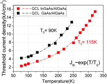
Figure 13. Threshold current density as a function of temperature for In0.026Ga0.974As/AlGaAs QCL (red symbol/line) and GaAs/AlGaAs QCL (black symbol/line).
Download figure:
Standard image High-resolution imageThe differential slope efficiency in temperature range from 77 K to above RT (323 K) for the In0.026Ga0.974As/AlGaAs QCL and GaAs/AlGaAs QCL is shown in figure 14. The devices show a drop in the slope efficiency as temperature increases. For In0.026Ga0.974As/AlGaAs QCL we observed that η = 1.3 W A−1 at 77 K decreases to η = 0.08 W A−1 at 323 K, whereas for GaAs/AlGaAs QCL we observed that η = 0.6 W A−1 at 77 K decreases to η = 0.01 W A−1 at 270 K. The slope efficiency characteristic temperature equals T1 = 222 K for In0.026Ga0.974As/AlGaAs QCL and T1 = 134 K for GaAs/AlGaAs QCL, which again confirms superior high temperature performance of In0.026Ga0.974As/AlGaAs QCL. The wall-plug efficiency (WPE) for both types of QCLs is shown in figure 15. The peak WPE for In0.026Ga0.974As/AlGaAs QCL laser equals 9.94% and 2.6% per facet at 77 K and at 250 K respectively whereas for GaAs/AlGaAs QCL it equals 5.6% and 0.3% per facet at 77 K and 250 K, respectively.
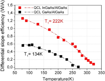
Figure 14. Differential slope efficiency as a function of temperature for In0.026Ga0.974As/AlGaAs QCL (red symbol/line) and GaAs/AlGaAs QCL (black symbol/line).
Download figure:
Standard image High-resolution image
Figure 15. WPE for GaAs/AlGaAs QCL (black lines) and for In0.026Ga0.974As/AlGaAs QCL (red lines) at T = 77 K (solid lines) and at T = 250 K (dashed lines).
Download figure:
Standard image High-resolution imageFigure 16(a) presents spectra registered at 77 and 295 K for In0.026Ga0.974As/AlGaAs device. Spectra for GaAs/AlGaAs device were registered at 77 and 245 K and are shown in the figure 16(b). The laser emission was collected using reflective objective to maximize collection efficiency. Emission spectra were registered using Nicolet 8700 Fourier Transform IR Spectrometer equipped with high sensitivity LN2 cooled MCT detector, working in rapid scan mode with resolution of 0.125 cm−1.

Figure 16. Emission spectra for In0.026Ga0.974As/AlGaAs QCL registered at 295 and 77 K at I = 1.05 Ith (a) and for GaAs/AlGaAs QCL registered at 245 and 77 K at I = 1.05 Ith (b).
Download figure:
Standard image High-resolution imageFor strained In0.026Ga0.974As/AlGaAs QCL the multimode emission registered at room temperature (295 K) is centred at 1009.46 cm−1 (9.91 μm) with mode spacing Δν = 0.76 cm−1. The emission at 77 K is centred at 1063.24 cm−1 (9.41 μm). For GaAs/AlGaAs QCL the multimode emission registered at the maximum operating temperature (245 K) is centred at 1018.1 cm−1 (9.82 μm) with mode with practically the same mode spacing as for In0.026Ga0.974As/AlGaAs QCL. The emission at 77 K is centred at 1044.7 cm−1 (9.57 μm).
4. Discussion
The numerous attempt aimed at lowering threshold current density and increasing maximum operation temperature for GaAs based QCLs with modified band offset are reported in the literature. The appropriate band structure modifications have been done either by introducing small amount of In into QWs in the active region [11], inserting InAs monolayers in the device active region and using AlAs barriers [12] or increasing the height of a single barrier in each active region [8]. In all cases, no indium was added to the injectors in order to keep the overall strain at low level. However, no substantial improvement of laser parameters was observed. The rapid increase of the threshold current density at higher temperatures for In modified GaAs/AlGaAs QCL was explained as being driven by thermal activation of tunnelling of electrons in the active region and increasing carrier leakage from the injector into continuum or by misalignment between injector and active cell. It can be seen, that all proposed modifications of the structure have not resulted in the improvement of laser's parameters. Until now, however there was no attempt to consistently deepen all the GaAs wells in the structure, both in the active region and in injectors. It turns out that this approach is leading to lasers with record parameters in their class. The In0.026Ga0.974As/AlGaAs QCLs exhibit low threshold and emit radiation at much higher temperatures than standard GaAs/AlGaAs QCLs, reaching maximum working temperature of 323 K (50 °C). For the reference, GaAs/AlGaAs QCLs the maximum working temperature rarely exceeds 0 °C. Comparison of the main electro-optical parameters for In0.026Ga0.974As/AlGaAs QCL and reference GaAs/AlGaAs QCL is presented in table 2.
Table 2. Comparison of the electro-optical parameters of In0.026Ga0.974As/AlGaAs and reference GaAs/AlGaAs QCLs.
| GaAs/AlGaAs QCL | InGaAs/AlGaAs QCL | |
|---|---|---|
| Jth (77 K) | 4.2 (kA cm−2) | 2.2 (kA cm−2) |
| Jth (250 K) | 13.3 (kA cm−2) | 7.3 (kA cm−2) |
| T0 (77–300 K) | 90 (K) | 115 (K) |
| WPE (77 K) | 5.6% | 9.94% |
| η (77 K) | 0.6 W A−1 | 1.3 W A−1 |
| TMAX.OPER. | 273 K (0 °C) | 323 K (50 °C) |
| PPEAK (77 K) | 2.2 W | 5.2 W |
| PPEAK (250 K) | 90 mW | 1.1 W |
We have also fabricated lasers from partially relaxed epi wafer with 3.77% of indium in the QWs. LIV characteristics for an In0.038Ga0.962As/AlGaAs QCL are shown in figure 17.

Figure 17. LIV characteristics of In0.038Ga0.962As/AlGaAs QCL. The data were collected in temperature range from 77 K to RT (293 K). Lasers with uncoated facets were investigated.
Download figure:
Standard image High-resolution imageThe lasers still operated at 300 K but with already higher average threshold current, i.e., 18.0 kA cm−2 comparing to 12.5 kA cm−2 for 2.64% of indium in QWs lasers (see figure 18). Further increase of In content resulted in rapid deterioration of laser parameters.
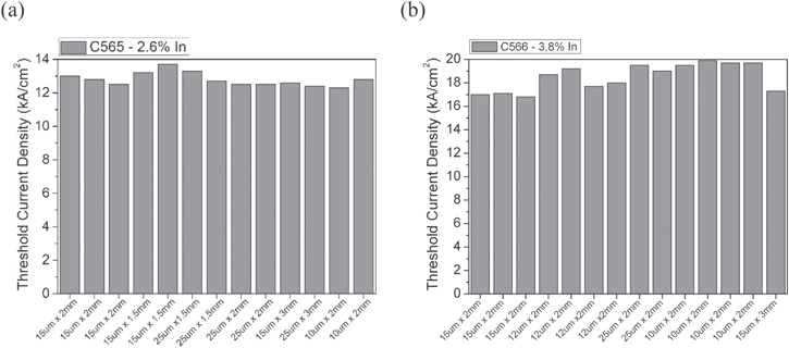
Figure 18. Histograms of room temperature threshold current density for the lasers with different cavity dimensions fabricated from the epi wafer with In content 2.64% in the QWs (a) and 3.77% of In in the QWs (b).
Download figure:
Standard image High-resolution imageIn the following paragraphs, we will discuss possible explanation of InGaAs/AlGaAs laser parameters improvement. Providing that we do not exceed critical concentration leading to strain relaxation addition of few percent of In to GaAs QWs increases band offset and consequently the activation energy for electron escape to continuum as well as leads to interface smoothing. Simple estimations show that the increase of activation energy for carrier escape from the upper laser level cannot account for twofold decrease of the threshold current. Therefore, the claim about interface–roughness (i–r) reduction as the major mechanism leading to improved performance of InGaAs/AlGaAs had to be confirmed by more advanced modelling.
We have employed non-equilibrium Green's functions method to examine electronic transport and optical properties of these devices. The use of NEGF modelling is very appropriate for this purpose as this method originates from the 'first principles' and allows for few parameters being adjusted while fitting simulations to the experiment. Then, if good agreement between experiment and simulation is achieved the parameters used in the simulation can be treated as reasonable/reliable estimates of these parameters. In the implementation we use, the only adjustable parameters are those characterizing correlation function of i–r potential which makes NEGF method a powerful tool of their estimation. We have applied this strategy to the devices under consideration. For both cases, we tested the same 'shape' of the correlation function and allow only for the change of the rms roughness height Δ. The final result we got: Δ = 0.19 nm for GaAs device and Δ = 0.07 nm for InGaAs device fully confirm our claim. In the following some details and results of simulations are presented.
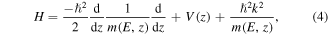
The NEGF implementation we use was fully described in our previous papers [28, 29]. It deals with one band 1D Hamiltonian which takes band mixing into account through energy dependent effective mass
where potential energy term V(z) comprises conduction band edge offsets Ec(z), external bias U, and the Hartree term calculated self-consistently by the solution of Poisson equation. Boundary conditions for the latter equation preserve charge neutrality of each QCL period. Calculations are made in the real space. The Hamiltonian (4) is discretized, and the grid points define its base vectors. This basis is quite large as the mesh of 76 grid points was used to map the QCL structure. The formulations for scattering self-energies in this basis were provided in [30–32]. For alloy disorder, LO-phonon, interface roughness and ionized impurity scatterings we use the formulations as in [32] whereas for the acoustic (LA) phonons we use energy averaged approximation following [30]. The only temperature in the model is the ambient (lattice) temperature, T (electronic temperature need not be introduced). The mentioned size of the basis refers to the central period of QCL device. The remaining parts are imitated by the left and right hand contact (retarded) self-energies ∑L,R. The problem is completely solved in k-space. Nonparabolicity of the subbands is included as in-plane energy terms involve bulk effective mass m(E) at the total (longitudinal + in-plane) energy [33]. Most of the parameters in the formulations for scattering self-energies is material or temperature dependent. As already mentioned the only parameters that are unknown and can be treated as adjustable are interface roughness correlation function shape, radius Λ and rms height Δ. Gaussian and exponential functions were tested and shown to be equivalent with a change of the parameters Λ and Δ [34]. So, in our comparative study we fix our choice at the Gaussian correlation function and the correlation radius value Λ = 9 nm, leaving Δ as the only adjustable quantity.
The adjustment for InGaAs/AlGaAs devices was done by fitting calculated and experimental I–V curves at two temperatures, 77 and 250 K. In figure 19 results of such fitting for InGaAs/AlGaAs device are shown. Devices for the comparison were selected to have overlapping I–V curves for different waveguide cross-sections (2000 × 15 μm2, 2000 × 25 μm2, respectively) what ensures that leakage currents are minimized.
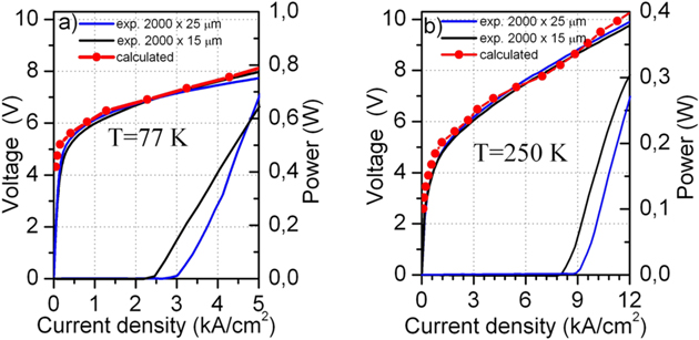
Figure 19. Experimental and calculated current–voltage–light characteristics at 77 K (a), and 250 K (b) for InGaAs/AlGaAs devices.
Download figure:
Standard image High-resolution imageAs can be seen very good agreement is achieved for the value Δ = 0.07 nm, that best matched experimental data. For this value, the experimental and calculated threshold currents also agree quite well. To estimate the latter total mirror and waveguide losses divided by the confinement factor (αm + αw)/Γ ≅ 60 cm−1 were assumed for 2000 × 15 μm2 waveguide [35] and compared to the calculated gain peak as demonstrated in figure 20(a). Good agreement for the threshold current was also found in the entire temperature range (see figure 20(b)).
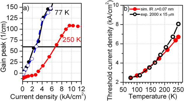
Figure 20. (a) Calculated gain peak versus current density at two temperatures compared to overall losses for 2000 × 15 μm2 waveguide divided by the confinement factor (αW + αm)/Γ ≅ 60 cm−1 (horizontal line). Filled and open symbols refer to InGaAs/AlGaAs and GaAs/AlGaAs device with the same value of rms (i–r) height Δ = 0.07 nm, (b) threshold current density measured for InGaAs/GaAs device compared to the simulations.
Download figure:
Standard image High-resolution imageOther results further confirm the agreement with the 'quantitative accuracy'; the calculated gain spectrum g(hν) for the same value of rms (i–r) height Δ = 0.07 nm, peaks at hν = 0.130 meV (λ = 9.54 μm) corresponding very well to experimental lasing wavelengths of λ = 9.4 μm at 77 K.
Similar analysis was performed for GaAs/AlGaAs device. Removing ternary alloy from the wells material resets the values of material parameters to its well-known binary estimates. Namely, mw = 0.067 for the effective mass and γw = 0.4 nm2 for nonparabolicity coefficient were taken instead of mw = 0.0654 and γw = 0.43 nm2 (which had been assumed for InGaAs device basing on the interpolation rules). These changes force the nonparabolicity coefficient in the barrier material drop to γb = 0.165 nm2 from γb = 0.169 nm2 (used for InGaAs material) as the relation γw/γb = (mb/mw)2 must hold [36]. Further changes include the decrease of the barrier/well band offset to 0.39 eV from 0.42 eV used for InGaAs device and cancelling alloy disorder scatterings in the well material. The latter for InGaAs devices were taken into account with a matrix element M = 1.12 eV equal to the band offset between InAs and GaAs [34].
When all these changes were introduced to the simulation structure while the i–r parameter Δ was remained unchanged (kept at the value of 0.07 nm), the change of the threshold current appears insufficient to fully account for the experimentally observed value. E.g. at 77 K it increases from Jth = 2.46 kA cm−2 to merely 2.80 kA cm−2 which is much lower than the value 3.85 kA cm−2 observed for GaAs devices. To clarify this issue the influence of the interface roughness on the device characteristics has been studied. Figure 21 shows calculated spectral gain for GaAs/AlGaAs device for different values of interface roughness parameter Δ. The general tendency observed is gain broadening and decreasing of gain peak with increasing interface roughness.
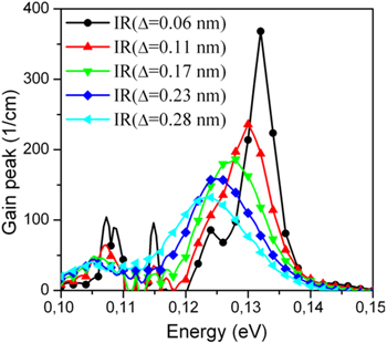
Figure 21. Calculated spectral gain for GaAs/AlGaAs device for different values of interface roughness parameter Δ.
Download figure:
Standard image High-resolution imageAs it has become clear that the gain spectrum is so strongly affected by interface roughness, threshold current density versus temperature for different values of (i–r) parameter Δ was calculated. The results are shown in figure 22. Good fitting with experimental data can be observed for rms height parameter value Δ = 0.19 nm.

Figure 22. The threshold current density versus temperature for GaAs/AlGaAs device for different values of interface roughness (i–r) parameter Δ.
Download figure:
Standard image High-resolution imageThe experimental and calculated current–voltage–light characteristics at 77 K for GaAs/AlGaAs QCLs for rms height parameter value Δ = 0.19 nm are shown in figure 23, while detailed analysis of electronic transport in GaAs device relaying on these simulations has been presented elsewhere [37].

Figure 23. Experimental and calculated current–voltage–light characteristics at 77 K for GaAs/AlGaAs QCLs.
Download figure:
Standard image High-resolution imageSimilarly to InGaAs/AlGaAs devices the GaAs/AlGaAs lasers selected for the comparison have overlapping I–V curves. Calculated gain peak versus current density at 77 K compared to overall losses divided by the confinement factor (αW + αm)/Γ = 60 cm−1 for GaAs/AlGaAs device is shown in figure 24(a). As can be seen, excellent agreement for I–V curve and threshold current versus temperature is observed in the entire temperature range (figure 24(b)).

Figure 24. Calculated gain peak versus current density at 77 K compared to overall losses divided by the confinement factor (αw + αm)/Γ = 60 cm−1 for GaAs/AlGaAs device (a), and threshold current versus temperature (b).
Download figure:
Standard image High-resolution image
The calculated gain spectrum g(hν), peaks at hν =0.126 meV (λ = 9.85 μm) corresponding very well to experimental lasing wavelength of λ = 9.6 μm, the calculated FWHM = 13 meV of the gain spectrum corresponds very well to the measured value 12 meV of electroluminescence below threshold.
5. Conclusion
In this work, we report on the design, fabrication and characterization of a mid-IR QCLs, based on InGaAs/AlGaAs structures grown by MBE Structures were grown with indium content from 1% to 6% in QWs and 45% of Al in AlGaAs barrier layers. The design results in strained heterostructure, however, no strain relaxation was observed as documented by x-ray diffraction measurements up to ∼3% of In content in QW. Optimum devices with 2.64% of indium in QWs exhibit performance largely improved over reference GaAs/AlGaAs QCLs. We have observed the reduction of the threshold current density by a factor of 2 at 77 K, and 1.5 at 300 K. Lasing at ∼9.45 μm was achieved in pulsed mode up to T = 50 °C. Devices showed good thermal performance with characteristic temperature T0 = 115 K. Obtained threshold current densities of 2.2 kA cm−2 at 77 K and 11.1 kA cm−2 at 300 K are the lowest reported for GaAs based mid-IR lasers. Reduction of the threshold current density is attributed mainly to the reduction of interface roughness scattering which accounts for roughly 85% of improvement; the rest might be attributed to the increase of activation energy for the escape of carriers from the upper laser state to 3D continuum. Further increase of In content in QWs resulted in deterioration of device parameters. The experimental work shows the potential of GaAs based QCLs to become useful sources of mid-infrared radiation for less demanding applications.
Acknowledgments
The authors would like to thank Dr Piotr Karbownik Dr Artur Trajnerowicz for fabrication of investigated QCLs.
This work was supported by the National Science Centre (NCN) grants: OPUS 9 UMO-2015/17/B/ST7/04015 (DP, KP, MB), PRELUDIUM 9, 2015/17/N/ST7/03936 (PG) and Rzeszow University of Technology, Department of Electronics Fundamentals Grant for Statutory Activity (GH, AK).