


Abstract
For the first time, we show the phenomenon of asymmetric light reflection at the reflecting layer incorporated in a linear, time-independent and non-magnetic two-dimensional (2D) photonic crystal (PC). The proposed reflector shows asymmetry in the reflection (and hence, in transmission), if incident and reflected ports are interchanged. The possibility shown here should be of interest from the point of view of basic optics and should have interesting consequences/applications in applied optics.
Export citation and abstract BibTeX RIS
Introduction
PC structures are being explored to achieve optical functionalities which are not possible by any other means. i) Beam propagation without divergence in linear optics regime (self-collimation) [1–3], ii) crossing of multiple beams with almost zero cross-talk [4], iii) two-ports [5–7], three-ports [8] and diffraction-inspired [9] asymmetric light propagation in linear, non-magnetic and time-independent materials are some examples of the functionalities which are shown to be possible with PC structures. Recently, a strong difference between the forward incidence and backward incidence has been shown to be possible for a sole linear, non-magnetic photonic crystals prism [10]. In short, asymmetric light propagation in linear, time-independent and non-magnetic structures has been an intriguing issue in basic as well as in applied optics mainly due to power-independent and non-magnetic features.
It is worth mentioning here that, for the purpose of implementation in a circuitry, an asymmetric device would have to have one input port and one output port for forward propagation such that the output port becomes the input port for backward propagation.
In this letter, for the first time, we show the phenomenon of asymmetric light reflection at the reflecting layer incorporated in a structure of 2D PC. The proposed reflector shows asymmetry in the reflection (and hence in transmission), if incident and reflected ports are interchanged.
Background
For the sake of clarity, we first discuss symmetric (conventional) reflection. Let us consider a conventional reflecting surface S. When an optical beam is incident in the direction X1O (say, from the incident port X1) on S as shown in fig. 1(a), some part of it is reflected in the direction OZ1 (it goes to the reflected port Z1) as per reflectivity R of the surface and the remaining part is transmitted in the direction OX2 (it goes to the port X2) as per transmittance T of the surface. If the situation is reversed, i.e., if the beam is incident in the direction Z1O (from the incident port Z1 as shown in fig. 1(b)), the reflected part goes in the direction OX1 (it goes to the port X1) and the transmitted part in the direction OZ2 (it goes to the port Z2). The reflection phenomenon in this case is symmetric as R and T do not change in both the situations. In other words R and T are invariant under the interchange of the incident ports X1 and Z1. Therefore, the behavior of a conventional reflector is symmetric under such an interchange.

Fig. 1: (a) When an optical beam is incident in the direction X1O on a conventional reflecting surface S as shown, some part of it is reflected in the direction OZ1 (it goes to the reflected port Z1) as per reflectivity R of the surface and the remaining part is transmitted in the direction OX2 (it goes to the port X2) as per transmittance T of the surface. (b) If the situation is reversed, i.e., if the beam is incident in the direction Z1O (from the incident port Z1), the reflected part goes in the direction OX1 (it goes to the port X1) and the transmitted part in the direction OZ2 (it goes to the port Z2). R and T in this case are invariant under the interchange of the incident ports X1 and Z1 and the behavior of a conventional reflector is said to be symmetric under such an interchange.
Download figure:
Standard imageProposed structure for asymmetric reflection
In what follows, we show the possibility of an asymmetric reflection phenomenon wherein R and T change if the ports X1 and Z1 are interchanged. This is shown to be possible at the reflecting layer incorporated in a linear, time-independent and non-magnetic structure of 2D PC. The possibility shown here should have interesting consequences/applications in applied optics.
The proposed structure to demonstrate the above-mentioned possibility is shown in fig. 2(a) which is based on a 2D square-lattice PC consisting of infinitely long circular rods of refractive index 2.9, embedded in the background of air. The diameter of the rods is  , where a is the lattice constant. The structure consists of
  layers in X and Z directions, respectively. For 2D transverse magnetic (TM) polarization (the electric field is parallel to the length of the rods, i.e., the Y-axis), Equi-frequency contours (EFCs) which are the cross-section of dispersion surfaces at constant frequencies [11], have been obtained using the plane-wave expansion (PWE) method [12,13] and are shown in fig. 2(b). It can be seen in the figure that the light beam would be self-collimated in
  and
and  for normalized frequency
  . A splitter/reflector layer has been created/incorporated by elliptic rods (rods of elliptic cross-section) marked in gray color. The diameter of the elliptic rods is
  and
and  , respectively, along the minor and major axis. In short, the PC offers a guiding medium to the optical input by self-collimation (so that the beam can be obtained as a useful output at output ports) and the layer of the rods of the elliptic cross-section acts as the asymmetric reflecting layer. We mention here that beam splitters/reflectors made up of a reflecting layer of circular rods (rods of circular cross-section) are available in the literature, for example, in [14–17]. The reflection phenomenon in these references is symmetric in nature.

Fig. 2: (Color online) (a) The proposed structure to show asymmetric reflection phenomenon, wherein R and T change if the incident ports are interchanged, is based on a two-dimensional square-lattice photonic crystal consisting of infinitely long circular rods of diameter  and of refractive index 2.9, embedded in the background of air. The structure consists of
  layers in the X and Z directions, respectively. A splitter layer has been created by elliptical rods (rods of elliptic cross-section) of diameter
  and
and  . (b) Equi-frequency contours (for 2D TM polarization) for the proposed structure which are obtained using plane-wave expansion (PWE) method.
Download figure:
Standard imageIn order to analyze the reflection phenomenon in the proposed structure, we perform numerical experiments using a two-dimensional finite-difference time domain (2D-FDTD) method [18]. The well-known FDTD method is not discussed here for the sake of brevity. The whole structure is surrounded by perfectly matched layers (PML) [19,20] to avoid unwanted reflections from the simulation boundaries. The plane of propagation is the  plane. The spatial grid resolution in the X- and Z-direction is chosen as
  , i.e. 20 points per unit cell. The considered optical input is a TM polarized continuous-wave Gaussian beam of width 5a at full-width half-maximum (FWHM) of normalized frequency
  . Time-averaged power monitors MX1, MX2, MZ1 and MZ2 of width 15a have been configured to record the steady-state time-averaged power at the different ports.
Numerical investigation and discussions
We mention that FullWAVE (based on the FDTD method) and BandSolve (based on the PWE method) of the RSOFT Design Group, NY-USA, have been used to simulate/investigate the light propagation in the above-considered structure. Firstly, we launch a TM polarized continuous-wave Gaussian beam of normalized frequency  at port X1 as shown in fig. 3(a). As the EFC corresponding to the considered frequency is almost straight in the
  -direction, the beam is self-collimated in the PC in the
  -direction as shown by the steady-state electric-field distribution in the figure. When the beam reaches the splitting/reflecting layer, it splits into two orthogonal parts. One propagates towards the X2 port (transmitted) and the other towards the Z1 port (reflected). It can be seen in the figure that the portion of the incident light reflected towards Z1 is much larger than the transmitted portion reaching X2. The normalized steady-state time-averaged powers recorded by monitors configured at X2 and Z1 are 0.234 (23.4%) and 0.631 (63.1%), respectively. It is worth mentioning here that a very small portion of the light beam is also seen at the Z2 port (say, the isolated port) and the normalized steady-state time-averaged power at the Z2 port is found to be 0.097 (9.7%). It is worth clarifying here that the power launched from an optical source coupling into the photonic structure in the form of the self-collimated beam is the "injected power" which is 71.8% of the launched power in the present simulation. As the splitting/reflecting layer splits the injected power only, the normalization has been done with respect to the injected power, i.e., with respect to the steady-state time-averaged power of the monitor MX1 (shown in fig. 2(a)).
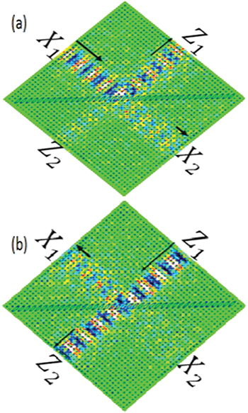
Fig. 3: (Color online) Panel (a) shows the propagation of a TM polarized continuous-wave Gaussian beam of normalized frequency  incident at port X1. The beam is self-collimated in the photonic crystal in the
  -direction and splits into two orthogonal parts at the splitting/reflecting layer. The normalized steady-state time-averaged powers recorded by monitors configured at X2 and Z1 are 0.234 (23.4%) and 0.631 (63.1%), respectively. Normalization has been done with respect to the injected power which is 71.8% of the launched power. (b) When the same input is injected at port Z1, the normalized steady-state time-averaged powers recorded at Z2 and X1 are 0.666 (66.6%) and 0.268 (26.8%), respectively. Normalization is done with respect to the injected power which is 79.9% of the launched power. Significant change of reflectivity R and transmission T confirms asymmetric reflection.
Download figure:
Standard imageWe now launch the same input at the port Z1 (which was the reflecting port in previous case). As can be seen in fig. 3(b), the beam is self-collimated in the  -direction (due to straight EFC corresponding to the considered frequency in the
  -direction). As per conventional reflection phenomenon, a larger portion of the light is expected at X1 and a smaller portion at Z2. However, as can be seen in the figure, a much larger portion propagates towards Z2 and a smaller one towards X1. The normalized steady-state time-averaged powers recorded at Z2 and X1 in this case are 0.666 (66.6%) and 0.268 (26.8%), respectively. For this case, the injected power, i.e. the steady-state time-averaged power (recorded at monitor MZ1) is 79.9% of the launched power. The isolated port is X2 where the normalized steady-state time-averaged power is observed to be 0.037 (3.7%). Obviously, the proposed structure allows for the asymmetric reflection phenomenon.
The origin of the asymmetric reflection phenomenon lies in the elliptic cross-section of the rods of splitting/reflecting layer. The splitting/reflecting layer "seen" by a light beam propagating in the  -direction is different from the same "seen" by a light beam propagating in the
  -direction. A light beam propagating in the
  -direction "sees" a diameter of the rods equal to
  , while it is
  for a light beam propagating in the
  -direction. Hence, the splitting/reflecting layer offers different reflectivity/transmission for beams injected from two perpendicular ports.
We go further and determine the response of the proposed structure with respect to the input frequency (frequency sensitivity). Figure 4(a) shows the variation of the normalized power recorded at coupled, reflected, transmitted and isolated ports with the variation of the normalized frequency when the input is launched at port X1. Figure 4(b) shows the same when the input is launched at port Z1. It may be noted in these figures that the proposed structure offers asymmetric reflection of light for a broad range of frequencies. It may also be noted that the sum of steady-state time-averaged powers at reflected, transmitted and isolated ports is almost equal to the total steady-state time-averaged power coupled to the incident port.
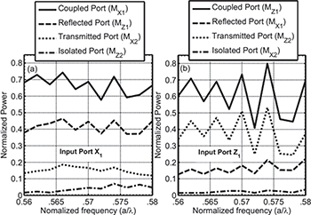
Fig. 4: Panel (a) shows the variation of the normalized power recorded at the coupled, reflected, transmitted and isolated ports with the variation of the normalized frequency when the input is launched at port X1. Panel (b) shows the variation of the normalized power recorded at the coupled, reflected, transmitted and isolated ports with the variation of the normalized frequency when the input is launched at port Z1.
Download figure:
Standard imageWe believe that the possibility discussed here might have potential applications in applied optics like signal routing.
Before the conclusion it is worth mentioning that 2D simulations have been carried out in this letter for the sake of brevity. A 2D simulation is useful for understanding the qualitative behavior of a true 3D device reducing the computation time, while, capturing the essential physics of the problem [21–23].
Conclusion
In conclusion, asymmetric light reflection at the reflecting layer of a linear, time-independent and non-magnetic two-dimensional (2D) photonic crystal (PC) has been shown to be possible in this paper. The PWE and FDTD methods have been used for numerical investigations. The proposed structure offers the asymmetric reflection of light for a broad range of frequencies. The possibility discussed here should be of interest in applied optics.
Acknowledgments
The authors acknowledge funding from Department of Science & Technology (DST), New Delhi, Government of India (SR/S2/LOP-0025/2012). The authors also acknowledge the critical comments of the anonymous reviewer for the improvement of the presentation of this letter.