


Abstract
We herein report the study of the atomic structure for a fully incommensurate CDW in LaTe2 using Cs-corrected scanning transmission electron microscopy (STEM). It is directly revealed for the first time that the atomic displacements adopt an incommensurate wave-pocket structure along each Te chain. This pocket structure has a long periodicity determined by the CDW incommensurability. We can use the sinusoidal waves as the first-order approximation to characterize the atomic motions within the pocket pattern, which can yield atomic displacements in good agreement with the theoretical model commonly used for studying CDW. These facts demonstrate that the incommensurate pocket patterns should be an essential structural nature in the CDW states and play a critical role for developing the mechanism of the CDW transitions.
Export citation and abstract BibTeX RIS
Introduction
In the past decades, a rich variety of quantum phenomena observed in strongly correlated materials, such as the high-temperature superconductivity and the colossal magnetoresistance, have been demonstrated to be essentially in correlation with the interplay among the degrees of freedom of electron, phonon, orbital and spin [1]. The CDW phenomenon is a typical cooperative phenomenon arising from strong coupling between electron and phonon in a quasi–one-dimensional (1D) or quasi–two-dimensional (2D) metallic materials [2]. Moreover, the CDW state often competes/coexists with other ordered states, such as superconductivity [3–5]. Although the mechanism of the CDW transition and periodic lattice modulations have been extensively studied in the past decades, direct imaging of atomic motion in the fully incommensurate CDW systems is indeed a challenging issue due to the presence of visible spatial anomalies in both the amplitude and phase of the modulation wave [6]. In order to understand the structural properties of the CDW systems, a variety of structural analyses have been performed by using X-rays, neutron and electron diffraction [6]. Actually, taking advantage of the strong interaction between incident electrons and the specimen, the electron diffraction and high-resolution TEM observations have obtained a rich variety of structural results for understanding the microstructure features of incommensurate states [6–8]. Importantly, recent developments of Cs-corrected STEM can be used to take chemically sensitive structure images at atomic level with a spatial resolution better than one angstrom [9].
Recent investigations in two-dimensional multiband systems suggest that certain CDW states show remarkable correlation with the momentum-dependent electron-phonon coupling rather than the conventional Fermi surface nesting [10,11] and the structural modulation has been quantitatively explained as commensurate domains separated by discommensurations (DC) or as a fully incommensurate state in a typical system [12,13]. LaTe2 has quasi-tetragonal crystal structure composed of alternating single pure Te sheets and double layers with staggered La and Te atoms along the c-axis direction, as shown in fig. 1(a). LaTe2 shows an incommensurate CDW modulation with a vector  at room temperature by means of TEM and single-crystal x-ray diffraction [14,15]. This modulation is proposed to be a one-dimensional transverse wave along the a-axis and the atomic displacements occurs within the Te sheets [14,15]; this structural feature makes LaTe2 an elegant simple model for STEM observations to directly address the atomic motion in the fully incommensurate CDW state. Herein, we reported on the experimental results for LaTe2 obtained by using Cs-corrected STEM. An incommensurate wave-pocket structure for the first time has been demonstrated to be the essential structural pattern in the CDW state.
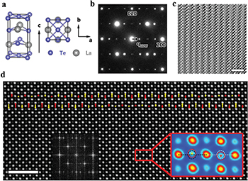
Fig. 1: (Colour online) Crystal structure and CDW modulation in LaTe2. (a) Structural model of the layered LaTe2 crystal. (b) Electron diffraction patterns taken along the [001] zone axes, showing the incommensurate modulation along the a-axis. (c) Conventional high-resolution TEM image, showing the modulation in association with the CDW. Scale bar is 2 nm. (d) Atomic-resolution HAADF-STEM image of LaTe2. The bright dots correspond to the La/Te columns (big dots) and Te columns (small dots), respectively. Arrows (yellow and red) indicate the motions of Te atoms. The inserted image on the right side shows a magnified figure for two unit cells, illustrating the displacements of Te atoms. Scale bar is 2 nm. The inset image of the left side gives a fast Fourier transform of the STEM image from a relative larger area.
Download figure:
Standard imageExperimental
The single crystals in the present study were grown by using a self-flux method. The TEM/STEM experiments were performed in the JEOL ARM200F equipped with double aberration correctors and cold field emission gun operated at 200 kV. The average displacement of La(Te) and Te column centers is determined by fitting as two-dimensional Gaussians using the MATLAB software. Firstly, the STEM image is automatically divided into many rectangular blocks whose edges correspond to local intensity minimum and there is just one column in each block. Then, for each block, the weighted average position of all pixels is calculated and is set to be the initial value for an iterative process which optimizes the two-dimensional Gaussian function. During this process, the fitting tolerance is set to be 0.0001. Finally, the optimized peak position is regarded as the exact center of atomic column.
The electronic structure calculations were performed by using the full-potential linear augmented plane-wave (LAPW) method within density functional theory (DFT) via the well-known WIEN2K package. The exchange correlation potential was treated by the generalized gradient approximation (GGA). The muffin-tin radii are set to 2.3 and 2.2 for La and Te atoms, respectively, and RKmax was set to 7 to determine the basis size. The static susceptibility was calculated based on the DFT band structure. The density functional perturbation theory was used to perform the phonon calculation via the QUANTUM-ESPRESSO package. The self-consistent electronic structure calculations were carried out by using the norm-conserving pseudopential method. The 20 × 20 × 10 grid was used to generate the k points for the electronic structure, and the 4 × 4 × 2 phonon-momentum grid was used to calculate the dynamic matrices. The kinetic energy cutoff for wave function and density was set to 35 and 140 Ry, respectively.
Results and discussion
The CDW in LaTe2 occurs along the a-axis direction as clearly illustrated by using the electron diffraction (fig. 1(b)) and HRTEM observations (fig. 1(c)) taken along the [001] zone-axis direction. The main diffraction spots with relatively strong intensity in the diffraction pattern are the basic Bragg reflections from the average structure with a tetragonal unit cell as illustrated in fig. 1(a). It is noted that each main spot is followed by a series of satellite reflections characterized by a modulation wave vector of  , where
  is the incommensurate parameter illustrating the disproportionate correlation between basic lattice and the CDW periodicity as discussed in the following context. In general, a periodic contrast alternation can be clearly observed by a conventional high-resolution TEM image as shown in the fig. 1(c); on the other hand, it is well known that the atomic contrast in the TEM image is sensitive to imaging conditions, such as the sample thickness and defocus values, and it is often difficult to directly detect the small atomic motions for specific atoms within a CDW modulation. Additionally, our experimental results also show that the electron diffraction pattern taken along the [010] zone direction does not exhibit any superstructure spots, indicating that the CDW in LaTe2 is accompanied with a well-defined transverse modulation in which the atomic displacements occur along the b-axis direction in agreement with the reported data in ref. [15].
In order to better and more clearly view the atomic structural features and, in particular, the atomic motions associated with the CDW in the Te layer, we take the advantage of the atomic-resolution high angle annular dark field (HAADF) STEM images. As a result, our careful measurements on the STEM images taken from a number of thin areas demonstrate the existence of remarkable atomic shifts for certain Te atoms. Careful analysis suggests that the atomic displacements mainly occur in the Te layer which are not only governed by the CDW wave but also affected visibly by the presence of incommensurability. Figure 1(d) shows a typical Cs-corrected STEM image taken along the [001] zone-axis direction clearly exhibiting the atomic structure of a LaTe2 crystal in which the incommensurate modulation is characterized by using electron diffraction (fig. 1(b)). It is known that the dot brightness in the HAADF image for an atomic column is proportional to Zn (1 < n < 2, Z is the atomic number) [9], therefore it is distinguishable that the large bright dots arranged in a square lattice are the projection of the La/Te atomic columns in which the La and Te are arranged alternatively along the view direction, and the small dots are Te atoms in the Te layer in the structural model as shown in fig. 1(a). It is distinguishable that the Te-atom positions show periodic deviations from the center of the La(Te) square lattice. In fig. 1(d), the direction and length of the arrows (yellow and red) schematically indicate the direction and amplitude of the atomic displacements.
We now proceed to investigate local atomic structural distortions for incommensurate modulations in LaTe2. It is well known that the accurate measurement of atomic displacement in STEM analysis is primarily limited by the signal-to-noise ratio (SNR) and scanning instabilities [16–19]. Previously, these issues have been discussed based on some theoretical approaches by averaging numerous image frames to reduce instabilities and increase SNR [17]. Very recently, sub-picometre (pm) precision measurements of atom positions have been successfully obtained by using a non-rigid (NR) registration scheme [19]. In the present study, we have improved our experimental measurements by using a model-based approach. According to our experimental results and previous reported data, the CDW modulation chiefly appears in the Te layers and no notable atom motions occur in the LaTe layers, therefore we can well measure and specify Te displacements in the STEM image by a deviation vector from the central position of La(Te) lattice as typically indicated by arrows in fig. 1(d) and clearly illustrated in the inserted image, in which two adjacent La(Te)-column dots are used as the internal standard to calibrate STEM instabilities during imaging. In order to simplify our analysis on the Te motion within the CDW state, we have artificially wiped out all atom images arising from the La(Te) blocks in an experimental micrograph, then we also disproportionally enlarged the displacement value by 3.5 times along the b-axis direction so that the local atomic displacements and specific modulation wave patterns can be clearly illustrated, as shown in fig. 2(a). It is remarkable that the atomic motions are strongly modulated in both amplitude and phase by a long-period wave; moreover, the resultant atomic structure shows visible long-periodic pocket chains along the CDW direction, and adopts an out-of-phase configuration stacking along the b-axis direction resulting in an energetically preferred centered structure.
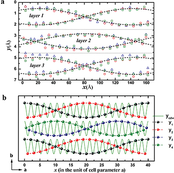
Fig. 2: (Colour online) Experimental data for atomic motions, incommensurate wave pockets, and sinusoidal wave behavior for Te atoms in the CDW state. (a) Experimental data for the Te displacements obtained from three different areas, Te displacements along the b-axis directions have been enlarged for clarification. The pocket pattern adopts an out-of-phase configuration yielding an energetically preferred centered structure. (b) The atomic motions were characterized by the sinusoidal waves  (δ is the incommensurate parameter,
  ,
,  , π,
, π,  and
and  ) as the first-order approximation. Moreover, the incommensurate modulation
  as commonly used to study the CDW structure is also shown for comparison.
Download figure:
Standard imageTheoretical analysis and experimental measurements on the atomic displacements in the Te layers reveal that the atom motions can be addressed by using the sinusoidal waves as first-order approximation, so four sinusoidal waves are shown in fig. 2(a) to address the fully incommensurate modulation in the Te layer. These modulations with a long period of  go along the a-axis direction, showing an amplitude of about 22 pm corresponding to the largest off-center atomic displacement as observed in our experiments. In fig. 2(b), we show a schematic illustration for the relationship between the four modulation waves, which can be written as
  ,
,  ,
,  and
and  , respectively, where the incommensurate parameter
  . It is recognizable that the atomic motion can be well addressed by the wave pockets, and our further analysis shows that the simulated electron diffraction pattern well reproduces the experimental patterns.
In previous literatures, the incommensurate CDW modulations are commonly described theoretically as a simple sinusoidal wave for fitting the diffraction data [6,12,20,21]. For instance, the CDW in LaTe2 can be expressed as  . In order to apparently illustrate the correlation between the wave-pocket structure and the CDW sinusoidal wave, we clearly show both pictures in fig. 2(b), careful analysis suggests that at the Te atomic positions, i.e.
  (n is an integer),
  can be satisfied, in addition,
  ,
,  , and
, and  can also be, respectively, satisfied for specific Te atoms in the Te layer. This fact suggests that though the sinusoidal wave model for incommensurate modulations does not pay specific attention to local atomic motion, it is well consistent with the pocket wave pattern as first-order approximation as revealed in our experiments, therefore, the main diffraction data can be successfully indexed and simulated based on
  as reported in previous literatures [20,21].
In order to further illustrate the relationship between the atomic displacements in the CDW states, we have performed a series of measurements and microstructure analysis on Sr doping samples which also show the CDW modulation with different periodicities. Indeed, slightly Sr doping can tune charge concentration and yield certain changes in the CDW modulation. In fig. 3, we show the electron diffraction data taken from three typical La1−xSrxTe2 samples with  , 0.05, and 0.08. We get three modulation vectors, i.e.,
  ,
,  and
and  , respectively, as shown in fig. 3(a)–(c); the atomic displacements associated with the CDW states are clearly illustrated in the left column. It is a recognizable that for
  in the LaSr0.05Te2 sample, the CWD wave has a well-defined superstructure and no pocket pattern can be observed. The pocket structure for
  is illustrated in fig. 3(c), it shows very similar features with what discussed for the LaTe2 sample in the above context. We therefore conclude that the incommensurate pocket wave could be a common structural nature in the fully incommensurate CDW systems, and atomic displacement in this modulated structure results from notable electron-phonon coupling.
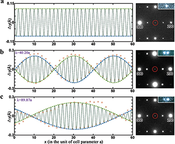
Fig. 3: (Colour online) Displacements of Te atom in the Sr-doped samples with different CDW periodicities:  in which (a)
  , (b)
, (b)  , and
, and  . (a) A typical superstructure state is obtained at La0.95Sr0.05Te2. (b) and (c): two different CDW states illustrating the visible incommensurate pockets with different periods. Two sets of experimental data obtained from a STEM image is also shown in fig. 3(b), (c) illustrating pocket structure with long period. The electron diffraction patterns are shown in the right column.
Download figure:
Standard imageIt is also noted that the local structure features in the CDW states in RETe3 are interpreted by the oligomers model in which the Te-Te bond lengths are simply characterized by the short and long Te-Te distances in the Te sheets [22]. Based on data as measured from our STEM images, we also performed a careful analysis on the bond lengths distribution; our analysis revealed that the bond distribution in the CDW state depends on a variety of factors, such as the incommensurability, crystallographic symmetry and direction of atom shifts. Our data also exhibits the oligomerization structure of the Te lattice of LaTe2 at a bonded/nonbonded threshold of 3.15 Å (not shown here); the radial distribution function for the bond lengths adopts a remarkable distribution centered at 3.15 Å and has a nonlinear change in the pure Te sheets, which indeed shows certain similarity with the data obtained for bimodal structure [22]; the CDW modulation in CeTe3 has been affected by the existence of interlayered coupling, so the complex structural distortions are explained by using the "trimers" and "tetramers" in an incommensurate CDW state [22].
On the other hand, it is well known that the microstructure features and structural modulations have been extensively studied by McMillan for the 1D incommensurate CDW [23–25]. It is demonstrated that strong electron-phonon coupling often lead to a discommensurate (DC) rather than uniformly incommensurate state, the discommensurations (so-called soliton) yield rapid phase change and interchain interactions may result in alignment of the discommensurations to form arrays of planar defects along CDW direction [25]. In contrast, the fully incommensurate state in LaTe2, as well as LaTe3, does not show lock-in phase transition at low temperatures. Our experimental results demonstrate that visible alternations in wave amplitude appear apparently associated with the CDW incommensurability and an incommensurate pocket waves instead of the DC domains become evidently visible in the present layered system.
In order to understand the fundamental structural features of the CDW state in LaTe2, we have performed first-principle calculations for the electronic structure and Fermi surfaces. LaTe2 is a multi-band system with two electronic bands crossing the Fermi level [20,21]. The electronic states near the Fermi level are dominantly occupied by the Te-5p derived orbitals from the Te sheets. Even though LaTe2 has a layered structure with a quasi–two-dimensional band structure, the Fermi surface shows a "hidden" one-dimensional feature as recognizable by intersecting 1D Fermi sheets, which is similar to that in CeTe3 [10,26]. In addition to the small electron pocket around the Γ-point, as shown in fig. 4(a), there is a nearly perfect FS nesting between two of the quasi-1D sheets along the (110) direction of the Brillonin Zone (BZ), as indicated by the arrow  . Therefore, a Fermi surface nesting driven CDW modulation is expected to occur along the [110] direction. However, the experimental observations clearly shows that the CDW modulation in LaTe2 goes along the [100] direction, as shown in fig. 4(b). In addition, we also performed a calculation on the static susceptibility and examined the CDW divergence, it is shown that the Fermi surface nesting vector does not carry over into the real part of the susceptibility
  , as shown in fig. 4(c). On the other hand, a maximum corresponding to a vector parallel to
  is observed, as indicated by the red arrow, which can be taken as an imperfect nesting vector in the Fermi surface. This vector is consistent with the CDW modulation
  observed in our experiment. It must be noted that the contribution of the interband transition has to be included in order to get such features, indicating that the finite-energy transitions are crucial in the formation of an ordering state, as discussed in CeTe3 and NbSe2 [10,27]. These facts suggest that the strong electron-phonon coupling associated with the structure distortions may play the predominant role for the CDW instability in the layered LaTe2 system [28–35]. In contrast to CeTe3 with a well-defined maximum in
  , the susceptibility
  of LaTe2 shows a series of maxima at around
  and
and  [10,20], therefore, different modulation vectors slightly deviated from
  or
or  can be also stable depending on the charge concentration as observed in the Sr doping samples (fig. 3). In addition, the electron-phonon coupling constant λ in the present case is estimated to be 0.235, which is well beyond the threshold value of 0.103 that separates the checkerboard from striped state [35], thus the stripe-like CDW pattern can be stable as observed in the high-resolution TEM images (see fig. 1(b)). Furthermore, considering the superconductivity
  occurring at low temperature or under a high pressure [36,37], we believe that the strong electron-phonon coupling in the layered LaTe2 plays an essential role for the appearance of phonon-mediated CDW superconductivity within a moderate coupling limit.
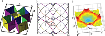
Fig. 4: (Colour online) First-principle electronic structure calculations for LaTe2 by DFT. (a) Three-dimensional Fermi surface in the first Brillouin zone. (b) Fermi surfaces at  , showing the "hidden" one-dimensional character, as indicated by the thick dashed orange line. (c) Real part of the static susceptibility as a function of
  ,
,  , with
  , calculated from the band structure by DFT. It was found that
  does not carry over and a series of maximum around
  emerges.
Download figure:
Standard imageIt is known that the CDW in one-dimensional systems or layered materials originates essentially from strong electron-phonon coupling. Therefore, the ordered electrons in the CDW phase could yield local atomic shifts which consist of longitudinal and transverse components. In the present case, LaTe2 adopts a layered structure and our TEM observations clearly show that the transverse components form a coherent structural modulation that can be well identified using Cs-corrected STEM images. On the other hand, longitudinal atomic shifts along the modulation wave vector direction are found to be much smaller than the transverse ones. Therefore, we can analyze the structural modulation in LaTe2 by using a transverse atomic wave.
In summary, we directly observed the atomic displacements associated with the fully incommensurate CDW state of LaTe2 using the Cs-corrected STEM. The structural analysis evidently demonstrated that the atomic motion adopts incommensurate pocket waves along each Te chain. This pocket structure has a long periodicity determined by the CDW incommensurability. Moreover, it is convenient to use a sinusoidal wave as first-order approximation to characterize the atomic motion; this approximation is fundamentally in agreement with the theoretical model used commonly for analyzing incommensurate CDW waves in low-dimensional systems. According to theoretical analyses, we conclude that the CDW instability in this layered system results from the strong electron-phonon coupling. It is expected that this CDW behaviors could be an important picture for understanding the lattice distortions associated with the incommensurate CDW.
Acknowledgments
This work was supported by National Basic Research Program of China 973 Program (Grants No. 2011CBA00101, No. 2015CB921300, No. 2011CB921703, and No. 2012CB821404), the Natural Science Foundation of China (Grants No. 11274368, No. 51272277, No. 91221102, No. 11190022, No. 11474323, and No. 91422303), and "Strategic Priority Research Program (B)" of the Chinese Academy of Sciences (No. XDB07020000).