


Abstract
The stability and band offsets of ZnO on c-plane AlN substrates with and without an Al-adlayer are studied by first-principles calculations. We determine the ZnO/AlN heterostructure by a layer-by-layer mode from the initial adsorption of the alternative layers of Zn and oxygen atoms of the first ZnO unit cell on c-plane AlN surfaces. The Al-adlayer occupies the top sites of AlN substrates and improves the ordered structure of the grown ZnO. The atomic charges, electronic density of states, and band alignment are systematically analyzed for the optimized ZnO/AlN heterojunction. The Al-adlayer induces in-gap states and causes the decrease of the band offsets for the Zn-terminated ZnO/AlN ( ) heterojunction.
Export citation and abstract BibTeX RIS
Introduction
Zinc oxide (ZnO) is a promising semiconductor material particularly for potential optoelectronic applications [1] due to its wide direct band gap in the near-ultraviolet region [2], a high exciton binding energy at room temperature [2], and piezoelectricity attributable to noncentral symmetry [3]. Aluminum nitride (AlN), with the largest direct band gap (6.2 eV [4]) among the III-nitride semiconductors, is quite promising as a substrate or buffer layer material for the epitaxial growth of ZnO due to its outstanding physical and chemical properties including high thermal conductivity [5], a high melting point (3273 K), and good lattice match with ZnO. AlN has a hexagonal wurtzite structure with experimental lattice parameters  and
and  [6], similar to that of ZnO (
 and
and  [7]). The experimental lattice mismatches between them are 4.50% and 4.55% for the a-axis and the c-axis, respectively, which is small and makes it possible to grow high-quality ZnO films on an AlN substrate.
For ZnO/AlN heterostructure [8–11] devices, knowledge of the energy band alignment and interfacial microstructure is of particular importance. The valence band offset (VBO) of ZnO/AlN heterojunctions [8] is determined by high-resolution x-ray photoemission spectroscopy to be  , with a type-II band line-up. The resulting conduction band offset (CBO) is
  . Wang et al [10] prepared heterojunctions of ZnO films on Si (111) substrates with an AlN buffer layer by using atomic layer deposition. The VBO was determined to be 0.83 eV for the ZnO/AlN heterojunction. The n-ZnO nanorod/p-Si heterojunctions (where "n" and "p" represent n- and p-type doping) with and without an AlN buffer layer were grown by radio frequency magnetron sputtering [11]. The CBO and VBO between ZnO and AlN are experimentally determined to be 3.29 eV and 0.83 eV in a ZnO/AlN/Si multilayer structure, respectively. Although the band offsets of ZnO/AlN heterojunctions have been investigated in the experiments, the accurate interfacial atomic structure and band alignment of AlN/ZnO are still unclear. In the present work we perform first-principles investigations of the stability and band offsets of c-plane ZnO/AlN heterostructure with and without an Al-adlayer.
Methodology
The structural and electronic properties of ZnO on c-plane AlN are investigated by employing ab initio density functional theory (DFT) calculations, as implemented in the Vienna Ab initio Simulation Package [12]. The generalized gradient approximation (GGA) with the Perdew-Burke-Ernzerhof (PBE) [13] is used to approximate the exchange-correlation potential and the valence electrons are separated from the core by use of the projector augmented-wave pseudopotentials [14]. We employ the PBE-GGA to optimize the atomic structure in the surface reconstructions. The electronic structure of the resulting energetically favorable reconstructions is then studied using a Heyd-Scuseria-Ernzerhof (HSE) hybrid functional [15] with a fraction α of Fock exchange of 0.38 [16,17] and a range separation parameter of 0.2 Å−1. The combination of the two functionals has been successfully used in previous studies [18,19]. One of the problems of hybrid functionals is the lack of rigorous criteria for the choice of the exchange mixing coefficient α, which should be a material-dependent parameter in principle [20]. This is an obvious problem for the heterostructure calculations, where potentially two or more different α need to correctly describe substrate and adsorbate. We therefore prefer to employ a single parameter for the heterostructure system. We adopt the cutoff energy of 600 eV for the plane-wave basis set. All the structures are relaxed until the forces acting on the atoms are less than 0.02 eV/Å. The criterion to stop the relaxation of the electronic degrees of freedom is set by both the total energy and the band structure energy differences between two consecutive steps to be less than 10−4 eV. The Brillouin-zone integrations are carried out with a Gaussian smearing [21] of  , and we employ a Monkhorst-Pack [22] sampling scheme with a k-point mesh of
  for bulk ZnO and bulk AlN. Within the above computational scheme, the optimized lattice parameters for ZnO bulk in the wurtzite structure are
  and
and  [23] (using the GGA). The DFT calculation predicts an energy gap of 3.33 eV for bulk ZnO, which is agreement with another theoretical value of 3.44 eV [17] and the experimental band gap of 3.3 eV [24]. The AlN lattice constants of the optimized wurtzite structure are
  and
and  [25]. The calculated direct band gap of AlN is 6.20 eV (using the HSE) and is consistent with another theoretical value of 6.19 eV [26] and the experimental value of 6.2 eV [4]. The theoretical lattice mismatches between ZnO and AlN are 4.76% and 5.48% along the a-axis and the c-axis, respectively.
A ( ) supercell with an atomic slab of six AlN bilayers and a vacuum region equivalent to 35.37 Å is used to model the AlN (0001) and (
 ) surfaces (see fig. 1). For the AlN (0001) surface, the pseudo-hydrogen atoms having a fractional charge of 0.75 passivate the dangling bonds at the bottom nitrogen layer in order to avoid the unphysical charge transfer between the top and the bottom surfaces of the slab. For the N-terminated surface, the dangling bonds at the bottom Al layer are saturated with pseudo-hydrogen atoms containing a fractional charge of 1.25 [27]. The internal electric field of the dipolar structure in wurtzite films can also be reduced by pseudo-hydrogen passivation [28]. The z-axis is perpendicular to the surface. The upper three bilayers of the slab and any adsorbate are allowed to relax, while the bottom three AlN bilayers and the saturating pseudo-hydrogen atoms are frozen in order to simulate the bulk-like substrate, after obtaining their stable positions optimized by a first relaxation step. The interface calculations are carried out with a
  Monkhorst-Pack mesh. The total energy differs by less than 0.01% after increasing the mesh to (
 ).
).

Fig. 1: (Colour online) Perspective view (middle) and top view of the AlN (0001) (right) and the AlN ( ) (left) surfaces with the high-symmetry adsorption sites indicated. Here "H3" and "T4" represent the threefold hollow site and the fourfold atop site, respectively, and "Top" is the top site on a surface Al or nitrogen atom.
Download figure:
Standard imageResults and discussion
The initial adsorption of the alternative layers of Zn and oxygen atoms of the first ZnO unit cell is now studied by a layer-by-layer mode [29,30] on the AlN (0001) and ( ) surfaces. We focus on the high-symmetry adsorption sites (see fig. 1). Based on the periodicity and symmetry of the hexagonal wurtzite structure, we adopt the H3 (threefold hollow), T4 (on top of a subsurface Al or nitrogen atom), and Top (on top of a surface Al or nitrogen atom) sites for the AlN (0001) and (
 ) surfaces [31]. The coverage is defined as the number of adatoms divided by the number of surface atoms. The total energies for Zn and oxygen layers on the AlN (0001) and (
 ) surfaces are calculated and the results are summarized in table 1. The results show that the Al-adlayer preferentially adsorbs on the top sites of AlN substrates. The first hexagonal ZnO unit cell cannot form on the perfect AlN (0001) surface because the alternative adlayers have not the desired hexagonal close-packed arrangement, while it is of interest to be grown after the introduction of an Al-adlayer. For the ZnO (
 ) surface the Zn-terminated ZnO ordered structure can be obtained on the substrate with and without an Al-adlayer. For both (0001) and (
 ) AlN surfaces, the Al-adlayer occupies the top sites and improves the ordered structure of the grown ZnO.
Table 1:.
The total energy (in eV) of Zn or oxygen layers on AlN (0001) and ( ) surfaces. The upper half of the table lists the Zn/O/Zn/O layer sequence being tested while the lower half lists the possible O/Zn/O/Zn layer sequence to be taken. The minimum total energy is taken as the zero energy reference.
| (0001) | ( ) ) |
||||||||||||
|---|---|---|---|---|---|---|---|---|---|---|---|---|---|
| H3 | T4 | Top | H3 | T4 | Top | H3 | T4 | Top | H3 | T4 | Top | ||
| Al-adlayer | 0.05 | 0.34 | 0 | 3.77 | 4.95 | 0 | |||||||
| 1st ML | Zn | 0 | 0.37 | 0.06 | 0.02 | 0 | 0.79 | 2.12 | 3.10 | 0 | 0 | 0.01 | 0.69 |
| 2nd ML | O | 12.01 | 0.32 | 0 | 0.71 | 12.61 | 0 | 0.18 | 0 | 9.25 | 13.27 | 0.68 | 0 |
| 3rd ML | Zn | 2.19 | 0 | 0.29 | 1.38 | 1.57 | 0 | 0.81 | 0 | 1.32 | 1.51 | 1.30 | 0 |
| 4th ML | O | 0 | 11.31 | 0.06 | 0.08 | 0 | 12.24 | 0.03 | 9.86 | 0 | 0 | 0.08 | 12.56 |
| (0001) | ( ) ) |
||||||||||||
|---|---|---|---|---|---|---|---|---|---|---|---|---|---|
| H3 | T4 | Top | H3 | T4 | Top | H3 | T4 | Top | H3 | T4 | Top | ||
| Al-adlayer | 0.05 | 0.34 | 0 | 3.77 | 4.95 | 0 | |||||||
| 1st ML | O | 0 | 4.03 | 5.01 | 0.19 | 0 | 17.35 | 5.20 | 9.22 | 0 | 0.06 | 0 | 20.84 |
| 2nd ML | Zn | 2.08 | 0 | 0.63 | 0.54 | 0 | 0.56 | 0 | 0.09 | 7.90 | 0.07 | 0.13 | 0 |
| 3rd ML | O | 0.61 | 7.23 | 0 | 0.16 | 15.90 | 0 | 8.82 | 0 | 0.46 | 0 | 0.02 | 16.44 |
| 4th ML | Zn | 0 | 0.63 | 2.56 | 1.00 | 1.15 | 0 | 6.27 | 5.06 | 0 | 0.08 | 0 | 0.09 |
The stability of defects at the surfaces is also considered to help understand the role they may play in heterostructure formation. We investigate the structures with defects employing ( ) AlN (0001) and (
 ) surface unit cells. These defects in our model are periodic arrays compared to the real surfaces; they do however provide some useful insight. In particular, we consider vacancies (one Al or nitrogen atom is removed from surface) and substitutional (the substitutional atom occupies the surface Al or nitrogen vacancy site) point defects. The defect surface formation energy [32,33] can be written as
  , where
  and
and  are the total energies of the relaxed defective and perfect slabs, respectively.
  and
and  are the excess (or deficit) number of atoms compared to the perfect slab, and the chemical potential of the corresponding atoms X in the slab, respectively. In equilibrium, the chemical potentials for Al or nitrogen in crystalline AlN are related through
 , where
  is the Al chemical potential corresponding to the face-centered-cubic bulk metal, and
  is the nitrogen chemical potential in its standard nitrogen gas state. The calculated values of
  and
and  are −3.74 eV and −8.30 eV as obtained by GGA calculations, respectively. The calculated formation enthalpy of hexagonal wurtzite AlN,
  , is found to be −2.85 eV, which agrees well with other theoretical values (−2.87 eV [26]) and is smaller in magnitude than the experimental value (−3.296 eV [34]). The Zn (or oxygen) chemical potential is set to Zn (or oxygen)-rich limit conditions, which can simulate the experimental environment. The surface formation energy of the AlN (0001) and (
 ) surfaces with defects is plotted within the allowed range for the chemical potential of nitrogen in fig. 2.The negative formation energy of VAl suggests that the creation of Al vacancies is spontaneous at AlN (0001) under N-rich conditions. However, the surface with substitutional Zn (ZnAl) has a lower energy than that of the Al vacancy. The predominant defects are thus ZnAl in the presence of Zn, which may result in a source of surface p-type behavior during growth. As the substitutional Zn adatoms on the AlN(0001) surface are from ZnO layer and the ordered ZnO unit cell cannot be directly obtained on the perfect AlN(0001) surface, we do not consider the effect of the interface ZnAl for ZnO/AlN(0001) interface with an Al-adlayer. For the AlN (
 ) surface, the surface point defects are unstable because formation energy is positive.
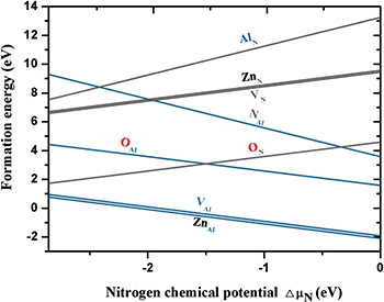
Fig. 2: (Colour online) The surface formation energy for defects at the AlN (0001) (cyan line) and ( ) (gray line) surfaces as a function of the excess nitrogen chemical potential,
  . Low values of
  correspond to N-poor conditions, while higher values are associated with high nitrogen pressures (N-rich conditions).
Download figure:
Standard imageFrom the results of the adsorption energy of the alternative layers of Zn and oxygen atoms of the first ZnO unit cell, we thus design the interface atomic arrangements of c-plane ZnO/AlN heterostructures (figs. 3 and 4). The ZnO/AlN heterostructures are modeled by a slab thickness of six ZnO atomic bilayers and six AlN atomic bilayers [35,36]. We use lattice constants  and
and  . All atoms in the heterostructures are allowed to relax in the calculations. The ZnO surfaces are saturated by fractional pseudo-hydrogen atoms [36]. For the relaxed Zn-terminated ZnO/AlN (0001) interface with the Al-adlayer (Zn/Al/Al) and the relaxed O-terminated ZnO/AlN (0001) interface with the Al-adlayer (O/Al/Al), the interplanar distances between the Zn/O interface plane and the Al-adlayer are 2.115 Å and 0.811 Å, respectively. For the relaxed Zn-terminated ZnO/AlN (
 ) interface (Zn/N) and the Zn/N interface with the Al-adlayer (Zn/Al/N), the interplanar distances are 1.988 Åand 2.078 Å, respectively, obtained from the Zn and Al/N positions. It can be seen that bonds are formed at ZnO/AlN interfaces from the isosurfaces of the interface charge densities in figs. 3 and 4.
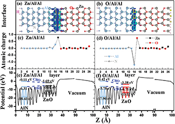
Fig. 3: (Colour online) The relaxed atomic structure with isosurfaces of the interface charge densities of the (a) Zn/Al/Al and (b) O/Al/Al interfaces (the yellow region represents charge accumulation, and the cyan region indicates charge depletion). The change of the atomic charges of the (c) Zn/Al/Al and (d) O/Al/Al interfaces compared to the bulk charges, and the planar average of the electrostatic potential for the (e) Zn/Al/Al and (f) O/Al/Al interfaces. Also shown as insets in the latter figures are the energy position and the value of the top edge of the valence band, the bottom edge of the conduction band, and the average of the electrostatic potential in the bulk-like region of each material.
Download figure:
Standard image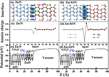
Fig. 4: (Colour online) The relaxed atomic structure with isosurfaces of the interface charge densities of the (a) Zn/N and (b) Zn/Al/N interfaces (the yellow region represents charge accumulation, and the cyan region indicates charge depletion). The change of the atomic charges of the (c) Zn/N and (d) Zn/Al/N interfaces compared to the bulk charges, and the planar average of the electrostatic potential for the (e) Zn/N and (f) Zn/Al/N interfaces. Also shown as insets in the latter figures are the energy position and the value of the top edge of the valence band, the bottom edge of the conduction band, and the average of the electrostatic potential in the bulk-like region of each material.
Download figure:
Standard imageTo determine the electron sharing in the various surface or interface structures, we calculate the numbers of electrons using the Bader topological charge analysis [37], where the charge density is partitioned by the interatomic surfaces characterized by the minimum charge density between two adjacent atoms. As the electron numbers do not give the exact value of valence electrons, we consider the difference between the atomic charges in the relaxed structures and those in the bulk to analyze the change in valence electrons (see figs. 3 and 4) [38]. The cation (anion) that gains electron density becomes more positive or less negative; the less positive or more negative value is associated with the more electrons in the cation (anion). The largest change occurs at the surface or interface of the ZnO/AlN heterostructures. The interface Zn and Al-adlayer atoms increase their electron density (by 0.78e and 0.27e, respectively) at the Zn/Al/Al interface, making them less positive. The interface Al-adlayer atoms decrease their electron density (by 1.19e), while the interface oxygen atoms acquire more electron density (0.75e) at the O/Al/Al interface. The interface nitrogen atoms decrease their electron density (0.34e) at the Zn/N interface, making them less negative. The interface Zn atom increases its electron density by 0.60e and the interface Al-adlayer atoms decrease their electron density by 1.09e at the Zn/Al/N interface. The interface Zn and nitrogen atoms in the Zn/N interface have more electron density after the interface Al-adlayer is introduced.
The band offsets of the ZnO/AlN heterojunction are determined by the electrostatic potential. The planar average of the electrostatic potential [39] V(x, y, z) in Cartesian coordinates can be expressed with the following equation:  , where the z-axis is perpendicular to the interface. Thus, the electrostatic potential V(z) is z-dependent and periodic in the xy-plane. Figures 3 and 4 show the variation of the planar-averaged electrostatic potential for the ZnO/AlN heterostructures. We perform a quantitative analysis of the band offset based on the planar-averaged electrostatic potential. The band offset values for the ZnO/AlN heterointerfaces are shown in table 2. The CBO and the VBO [40] are 3.56 eV and 0.68 eV for the perfect Zn/N heterostructure, respectively, which is in agreement with the experiment results [8,10,11]. Both the CBO and VBO decrease after the introduction of the interface Al-adlayer at the Zn/N heterostructure. We also note that the O/Al/Al and Zn/N heterostructures have a slope for the contour of the planar average of the electrostatic potential in the vacuum. This is likely due to different surface dipoles on the ZnO/AlN interface vs. the ZnO/vacuum interface, and will not converge for a longer cell.
The total density of states (TDOS) is analyzed for the ZnO/AlN heterostructures. The orbital nature of the interface in-gap states can be identified from the partial density of states. For the ZnO/AlN heterostructures with an Al-adlayer, in-gap states are observed in fig. 5 and are mainly derived from the interface Zn 3d4s and the interface O 2s2p states in ZnO, the Al 3s3p states in the interface Al-adlayer, and the interface Al 3s3p and the interface N 2s2p states in AlN. For the perfect Zn/N heterostructure there is an obvious band gap of about 3.08 eV, which shows that this interface maintains semiconductor properties and is free of in-gap states. The Zn-terminated ZnO/AlN ( ) heterojunction is predicted to be suitable for the design of ZnO-based semiconductor heterojunction field-effect transistors devices. The introduction of an Al-adlayer at the Zn/N heterointerface induces some in-gap states with Al 3s3p character.
Table 2:. Band offset values (in eV) for ZnO/AlN heterointerfaces.
| Present | Experiment | ||||||
|---|---|---|---|---|---|---|---|
| Zn/Al/Al | O/Al/Al | Zn/N | Zn/Al/N | ||||
| CBO | 1.58 | 3.80 | 3.56 | 2.33 |  [8] [8] |
3.66 [10] | 3.29 [11] |
| VBO | 1.29 | 0.92 | 0.68 | 0.55 |  [8] [8] |
0.83 [10] | 0.83 [11] |
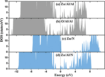
Fig. 5: (Colour online) The TDOS (not including pseudo-hydrogen atoms) of the ZnO/AlN heterostructure. The vertical dotted line gives the location of the Fermi level.
Download figure:
Standard imageSummary
The stability and band offsets of ZnO on AlN (0001) and ( ) substrates are studied using DFT. The initial adsorption of the alternative layers of Zn and oxygen atoms is determined by a layer-by-layer mode. The results showed that the Al-adlayer occupies the top sites of AlN substrates and improves the ordered structure of the grown ZnO. We also calculate the defective surface formation energy of point defects at the AlN surface. It is found that Zn atoms may substitute Al atoms and cause surface p-type behavior at the AlN (0001) surface. The electronic properties are calculated and analyzed for the ordered ZnO/AlN heterostructure. Based on the planar-averaged electrostatic potential, the CBO and the VBO are 3.56 eV and 0.68 eV for the perfect Zn/N heterostructure, respectively. Additionally, the Zn/N interface is free of some in-gap states. The interface Al-adlayer induces in-gap states and causes the decrease of the band offsets for Zn/N heterointerface.
Acknowledgments
This work has been supported by the Fundamental Research Funds for the Central Universities under Grant no. 2017XKQY092. We are grateful to the High Performance Computing Center of China University of Mining and Technology for the award of CPU hours to accomplish this work.