

Abstract
In recent years, the concept of shortcuts to adiabaticity (STA), originally developed for speeding up slow adiabatic state evolution in quantum systems, has found numerous applications in guided-wave optics. Optical waveguides, enabled by the advanced fabrication technologies, provide an ideal platform to implement the STA protocols in terms of geometry variations; moreoever, STA has enabled the development of short and robust waveguide components, with applications in beam couplers, beam splitters, mode converters, mode (de)multiplexers, and polarization manipulation devices. Concepts such as counterdiabatic driving, invariant-based inverse engineering, fast-forward approach, or fast quasiadiabatic dynamics, have been shown to provide shortcuts to adiabatic mode evolution in optical waveguides, resulting in compact functional devices with large bandwidth and fabrication tolerance. Novel devices have recently been fabricated following years of theoretical efforts, showing that STA have emerged as a new paradigm in optical waveguides. In this work, we discuss the major STA protocols for applications in optical waveguides and illustrate the shortcuts with device examples.
Export citation and abstract BibTeX RIS
Introduction
Light transfer among waveguides or guided modes is a ubiquitous functionality in optical waveguide devices. In general, there are two methods to realize light transfer in optical waveguides: resonant coupling [1,2] and adiabatic coupling [3,4]. In resonant-coupling–based devices, multiple supermodes of the waveguide structure with different propagation constants are excited, and the power transfer characteristics depend on modal interference in the devices. For example, in directional couplers [5,6] and multimode interference couplers [7–9], the desired split ratios can be achieved when the length of the device is at specific multiples or fractions of the beat length, with very short device lengths. However, the beat length is sensitive to wavelength and device geometry variations. So, resonant-coupling–based devices generally have small bandwidth and tight fabrication tolerance.
The operating principle of adiabatic-coupling–based devices is in general based on the slow evolution of a single waveguide mode caused by gradual changes in the device geometry [3,10,11]. If the geometry changes slowly enough, light remains in the mode even if the mode underwent significant evolution during propagation. Since the operating mechanism does not depend on a precise definition of power-transfer length and operating wavelength, an adiabatic (modal evolution) based device can in principle have large bandwidth and fabrication tolerance. However, adiabatic devices have to be sufficiently long to satisfy the adiabatic condition, and to minimize unwanted power transfer into other modes [12]. This, in turn, leads to longer device lengths in comparison to resonantly coupled devices and reduced component density, which is a major disadvantage in integrated optics based on densely integrated optical waveguides. There have been numerous approaches to optimize the geometry of adiabatic devices in order to reduce the device length [12–19]. One approach is to limit the fraction of power scattered into the unwanted modes below a constant value [13,17]. Another approach is based on the equalization of taper loss along each propagation step [14,16,18]. Various shape functions were also considered to minimize coupling between the adiabatic modes [12,15]. A recent systematic study on modal crosstalk in adiabatic couplers [19] compared two adiabaticity criteria [13,17] used in optical waveguides. Despite numerous efforts on the optimization of adiabatic devices, the lack of a simple set of design protocols makes it difficult to select the best design for a specific engineering application. In fact, the design problem is analogous to the problem of coherent quantum control [20], with the goal of performing precise and robust state transfer in a short time.
The recent development of shortcuts to adiabaticity (STA) in quantum control theory provides a framework to find fast routes to the final results of slow, adiabatic changes of the controlling parameters of a system [21,22]. At the same time, due to the analogies between quantum mechanics and wave optics [23], light propagation in waveguide structures has been used as a tool to visualize or investigate many coherent quantum phenomena which may otherwise be difficult to observe. The analogy can be exploited by describing field evolution in the devices by the coupled-mode theory, which is equivalent to the time-dependent Schrödinger equation describing the dynamics of an N-state quantum system. The first application of STA to optical waveguides was by Lin et al. [24], where counterdiabatic driving [25–27] was used to shorten mode conversion length in multimode waveguides; the same theory was later applied to a similar mode converter design [28]. A development in STA where a physically feasible alternative shortcut can be generated, called the "multiple Schrödinger pictures" approach [29], then solved the problem of physically unrealizable imaginary coupling terms in counterdiabatic directional couplers [30,31]. The Lie transform theory in Martínez-Garaot et al. [32] was used to design compact coupled-waveguide beam splitters unitarily transforming the formal results of counterdiabatic driving [33]. Invariant-based inverse engineering [34–36] was used to improve mode converter designs in multimode waveguides [37,38], coupled waveguide beam splitters [39], and asymmetric Y-junction mode-sorters [40] for reduced length and good robustness in subsequent works. The invariant-based approach was also applied to implement waveguide-based quantum logic gates [41]. Need-based designs were then made possible by the combination of the dynamical invariant and perturbation treatment [42–44], leading to directional couplers [45–47], mode (de)multiplexers [48], and polarization rotators [49] optimized against wavelength and/or fabrication variations. Using invariant-based inverse engineering, the adiabaticity of coupled-waveguide devices was optimized for short and robust designs [50], which also lead to the design of robust 3-dB couplers [51].
Beyond the coupled-mode theory formalism, the fast-forward approach [52] was used to extend the STA to full-wave regime in the design of ultra-compact waveguide junctions [53] and modal filters [54]. The fast quasiadiabatic dynamics (FAQUAD) approach [55] also went beyond the coupled-mode formalism, providing a shortcut design by homogenizing the adiabaticity using only one control parameter, which is beneficial in terms of fabrication. The FAQUAD approach was applied to the design of short and robust Y-junction mode splitters [56,57] and polarization mode conversion tapers for polarization splitting and rotation [58]. A similar rapid adiabatic coupling (RAC) scheme which suppresses modal crosstalk was also proposed to shorten the length of 3 dB couplers [59]. These theoretical investigations showed that STA in optical waveguides indeed provides a systematic route to optimize the design of adiabatic devices with short lengths and robustness against parameter variations.
With the fast development in theoretical efforts, experimental implementations soon followed. Integrated optics waveguide platform enabled by the advanced micro/nano fabrication technology provides an ideal platform to realize the device geometries designed by various STA protocols. The first demonstration was mode (de)multiplexers on silicon-on-insulator (SOI) [60] using invariant-based optimization [50]. The effort was followed by the demonstration of a compact broadband silicon 3 dB coupler [61] and a polarization splitter-rotator [62] using invariant-based inverse engineering [36,40]. FAQUAD-based 3 dB couplers were also fabricated on SOI, showing broadband characteristic and good fabrication tolerance [63]. A polarization splitter-rotator using a partially etched directional coupler was recently demonstrated on SOI [64] using invariant-based optimization [50]. The latest experimental demonstration is a short RAC coupler on SOI [65].
In this paper, we start with the coupled-mode theory formalism, introducing design protocols based on counterdiabatic driving and invariant-based inverse engineering. Following the introduction of dynamical invariants, need-based design approaches based on perturbation theory and optimization of adiabaticity are introduced. We then introduce the FAQUAD approach, which homogeneously distributes adiabaticity over the length of the device, speeding up mode evolution in adiabatic waveguide devices. Finally, we discuss the robustness of STA-based optical waveguide devices.
Coupled-mode theory
Under the scalar and paraxial approximation and assuming weak coupling, the changes in the amplitudes of N guided modes in a multimode waveguide, or N coupled single-mode waveguides, ![$|\Psi\rangle=[a_1, a_2,\ldots,a_N]^T$](https://content.cld.iop.org/journals/0295-5075/127/3/34001/revision1/epl19817ieqn1.gif) along the propagation direction z are described by the coupled-mode equation as [23]
along the propagation direction z are described by the coupled-mode equation as [23]

In multimode waveguides, the matrix elements of H(z) represent the coupling coefficients (complex-valued) between the guided modes enabled by waveguide gratings [66]. In coupled waveguides, the diagonal elements of H(z) describe the mismatch of the waveguides, and the upper and lower diagonal elements (real-valued) describe the coupling coefficients between neighboring waveguides (assume only nearest-neighbor coupling, the other matrix elements are zero). Replacing the spatial variation z with the temporal variation t, eq. (1) is equivalent to the time-dependent Schrödinger equation  describing the dynamics of an N-state system, and H is the Hamiltonian. We can rewrite eq. (1) in the adiabatic basis using a unitary operator Ua, and the resulting Hamiltonian in the adiabatic basis is
  . The first term
  is diagonal, and the adiabatic approximation neglects the second term to solve the uncoupled system in the adiabatic basis. So, the system evolution can be approximated by the adiabatic states, and the evolution can be designed by engineering H(z). If the adiabatic criterion is not satisfied, the system state cannot follow the adiabatic states, resulting in low conversion efficiency.
Counterdiabatic driving
A counterdiabatic term  can be added to H(z) to undo the effect of non-adiabatic coupling such that the system evolution follows the adiabatic states exactly even when the adiabatic criterion is not satisfied [25–27]. This was used to design STAs for short and robust mode converters in multimode waveguides [24,28] by superimposing additional gratings to implement the counterdiabatic term. However, for coupled waveguide systems, the Hcd term includes imaginary parts in the coupling coefficients that are not physically realizable. A way to generate feasible shortcuts is to perform unitary transformations U, such that the resulting Hamiltonian
 ![$U^{\dagger}[(H(z)+H_{cd})-i\dot{U}U^{\dagger}]U$](https://content.cld.iop.org/journals/0295-5075/127/3/34001/revision1/epl19817ieqn6.gif) is physically realizable. For two-waveguide couplers, the "multiple Schrödinger picture" transformation [29] was used to generate shortcuts for adiabatic directional couplers [30,31]. Beam propagation method (BPM) simulation of a counterdiabatic directional coupler is shown in fig. 1 [30]. A Lie-transform–based approach [32] was used to design arbitrary ratio three-waveguide beam splitters [33], and it can be generalized to generate compact beam splitters for N waveguides. In these devices, the key is to determine the corresponding waveguide geometrical variations specified by the Hamiltonian. In multimode waveguides, this relation corresponds to the periods and strengths of the superimposed gratings [66], while variations in waveguide spacings and widths are used to implement the Hamiltonian in coupled-waveguide systems [30].
is physically realizable. For two-waveguide couplers, the "multiple Schrödinger picture" transformation [29] was used to generate shortcuts for adiabatic directional couplers [30,31]. Beam propagation method (BPM) simulation of a counterdiabatic directional coupler is shown in fig. 1 [30]. A Lie-transform–based approach [32] was used to design arbitrary ratio three-waveguide beam splitters [33], and it can be generalized to generate compact beam splitters for N waveguides. In these devices, the key is to determine the corresponding waveguide geometrical variations specified by the Hamiltonian. In multimode waveguides, this relation corresponds to the periods and strengths of the superimposed gratings [66], while variations in waveguide spacings and widths are used to implement the Hamiltonian in coupled-waveguide systems [30].
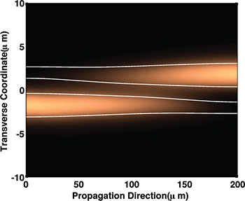
Fig. 1: BPM simulation of light propagation in a 200 μm counterdiabatic coupler [30]. Solid lines indicate the waveguide cores.
Download figure:
Standard imageInvariant-based inverse engineering
A dynamical invariant I, which satisfies ![$\partial_z I+(1/i)[I,H]=0$](https://content.cld.iop.org/journals/0295-5075/127/3/34001/revision1/epl19817ieqn7.gif) , gives the relation
, gives the relation  [67]. That is, acting on a solution of the Schrödinger equation, the invariant produces another solution of the Schrödinger equation. The result implies that an arbitrary solution of the Schrödinger equation can be written as a superposition of the eigenstates
  of the invariant. According to the Lewis-Riesenfeld theory [67], we can write
  , where
  is the Lewis-Riesenfeld phase, and cn is a time-independent amplitude. The fact that cn's are time-independent allows us to engineer the evolution of
  using the eigenstates of the invariant, which are now decoupled during the system evolution [34–36]. For example, the coupled-mode equation for a directional coupler consisting of two waveguides is

where Ω is the coupling coefficient, and Δ describes the waveguide mismatch. We can parameterize the eigenstates of the invariant as

and the orthogonal one (for all times  )
)

The system evolution is now described by these new parameters. To construct the Hamiltonian (specify the device parameters Ω and Δ) inversely, we substitute eqs. (3) or (4) directly into the Schrödinger equation (2), and find the following auxiliary differential equations:


These equations are equivalent to those obtained by the invariant dynamical theory [67], since  is a dynamical invariant with constants
  keeping the same unit as the Hamiltonian [42–44]. Using one of the eigenstates of the invariant, we can engineer the system evolution for the desired input and output states with an appropriate choice of boundary conditions. Figure 2 illustrates the various paths for mode conversion in a multimode waveguide using different paths designed by the invariant [38]. Mode converters in multimode waveguides [37,38] and coupled waveguide beam splitters [39] were designed using this approach. A short asymmetric Y-junction mode-sorter [40] based on this STA is shown in fig. 3.
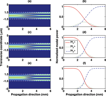
Fig. 2: BPM simulations of beam evolution in an invariant-based mode converter in multimode waveguide and their corresponding modal power evolution [38]. (a), (b): path A; (c), (d): path B; (e), (f) path C. Dashed white lines indicate the waveguide core.
Download figure:
Standard image
Fig. 3: BPM simulated mode sorting operation of the invariant based Y-junction mode sorter [40]. Input: (a) fundamental mode (b) second mode.
Download figure:
Standard imageNeed-based inverse engineering
In invariant-based inverse engineering, we can choose an arbitrary ansatz to interpolate the function θ, as long as the boundary conditions are satisfied. The freedom allows us to combine the inverse engineering and optimal control to select the most robust state dynamics in the presence of various noise and systematic errors for need-based device engineering [42–44]. A perturbation theory treatment was used to design directional couplers that are robust against wavelength or fabrication variations [45]. A directional coupler that is robust against both wavelength and fabrication errors was also designed [46]. We note that these approaches, while being robust against particular errors by design, do not guarantee adiabaticity. A design that is robust against a particular error might be highly susceptible to other sources of error. Another strategy is to use invariant-based inverse engineering to design the system evolution to be as close to the adiabatic state as possible, thus guaranteeing adiabaticity [50,68]. Adiabatic devices designed with this approach are now robust against various sources of errors, instead of only robust against specific errors by design. Figure 4 shows a short and robust directional coupler designed with optimized adiabaticity [50]. In addition, optimal control techniques can be applied to further improve the shortcuts [69].
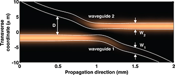
Fig. 4: Waveguide geometries and the corresponding BPM simulation for a short and robust directional coupler designed with optimized adiabaticity [50]. White lines indicate the waveguide cores.
Download figure:
Standard imageBeyond the coupled-mode formalism
The STA described so far have been limited to finite-dimensional systems where the dynamics of light transport can be reduced to coupled-mode equations, allowing a direct adaptation of STA protocols developed in quantum mechanics. However, the coupled-mode theory, based on the perturbation methods, is limited in its application to high index contrast waveguides such as the SOI. For applications to high index contrast waveguides, care must be taken to ensure that the device is working in the weak-coupling regime [48]. In Della Valle et al. [53], a STA for an infinite-dimensional system was developed based on the fast-forward approach [52]. Non-adiabaticity in the structure can be compensated by a suitable gradient refractive index profile. Another approach is to suppress modal crosstalk during system evolution [59,65]. Here, we review another full-wave approach based on the concept of adiabaticity engineering and fast quasiadiabatic dynamics (FAQUAD) [55].
Adiabaticity engineering
In quantum control, the "slowness" of the evolution of a system can be characterized by [70]

where c is the adiabaticity parameter, and  is the eigenvalue associated with Hamiltonian eigenstates
  or
or  . The same parameter can be used to quantify the adiabaticity of optical waveguides by replacing t with z in eq. (8). For two modes m and n in an optical waveguide, the adiabaticity parameter along any point of the evolution region for vectorial fields can be defined as [57]

where  and
and  are the transverse components of the electric field and magnetic field associated with the m-th and n-th eigenmodes of the optical waveguide,
  is the propagation constant associated with the m-, n-th eigenmodes, and S is the entire waveguide cross-section. Consider a single control parameter D(z) during evolution, we can relate the adiabaticity parameter to the control parameter by

where the chain rule  is used. F(D) is a measure of adiabaticity that is strictly related to the control parameter D. Assuming a monotonically changing D (
 0) and
  , we have

This result allows one to engineer the distribution of adiabaticity c(z) along the propagation direction using a single control parameter D(z).
FAQUAD
The FAQUAD protocol homogenizes the adiabaticity during the evolution by imposing a constant adiabaticity on the device  [55]. Rearranging the terms in eq. (11), we find
  which can be integrated to set the functional form of z(D) with the boundary conditions at the beginning
  and the end
  of the mode evolution region. For example, with the boundary conditions
  we have

with

To design F(D), we first look at the adiabaticity parameter clin of an evolution region with a linearly varying control parameter  . Using eq. (10), we can write

In a linearly varying evolution region, the adiabaticity parameter is decoupled from  , allowing us to solve for F(D) from the calculated clin using eq. (14). Finally, substituting eq. (14) into eq. (12) gives the FAQUAD design

Equation (15) describes how the original linear design is modified to obtain the control parameter in the FAQUAD design. We can see from the equation that when the linear clin is small (adiabatic), the device length changes less with  (the control parameter varies faster in z) in the FAQUAD design; and when clin is large (non-adiabatic), the device length changes more with
  (the device parameter varies slower in z) in the FAQUAD design. The protocol can thus homogenize the adiabaticity. The FAQUAD protocol was used in the design of asymmetric Y-junction mode (de)multiplexers [56,57] and a polarization splitter-rotator [58]. Figure 5 shows a FAQUAD 3 dB coupler fabricated on SOI.
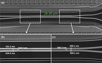
Fig. 5: A short and robust FAQUAD 3 dB coupler fabricated on SOI [63]. (a) SEM image of a FAQUAD 3 dB coupler with a  mode evolution region. (b) SEM image of the junction between Regions 1 and 2. (c) SEM image of the junction between Regions 2 and 3.
Download figure:
Standard imageDevice robustness
It is known that the conventional adiabatic designs require less precise control over waveguide parameters and have larger bandwidth, while on the opposite end, resonant coupling techniques require a very precise definition of the coupling length and coupling coefficient and have smaller bandwidth. So the question that naturally arises is: how the STA devices compare with the adiabatic devices and the resonant devices in terms of robustness to parameter variations? For the counterdiabatic couplers [30], it was shown that its tolerance is the same as the resonant coupler at the short length extreme, see fig. 6. As the device length increases, the tolerance of counterdiabatic couplers exceeds that of resonant couplers and is comparable to the adiabatic couplers; at the same time, the ripples seen in adiabatic couplers are reduced, indicating higher fidelity than adiabatic couplers. For even longer device lengths, the tolerance of counterdiabatic couplers becomes the same as adiabatic couplers because the counterdiabatic correction is negligible. For invariant-based devices, the devices can be engineered to have comparable bandwidth, fabrication tolerance, or both at shorter lengths than the conventional adiabatic designs [45–50,58]. The fabricated FAQUAD devices [63] also show large bandwidth and fabrication tolerance across an 8-inch SOI wafer, see fig. 7.

Fig. 6: Coupling efficiency against coupling coefficient variations for couplers designed using (a) adiabatic, (b) counterdiabatic, and (c) resonant coupling schemes [30].
Download figure:
Standard image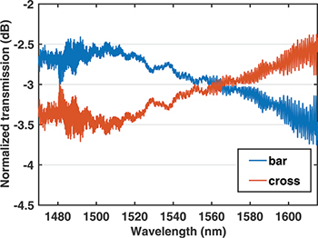
Fig. 7: Measured normalized bar and cross ports transmission coefficients of the fabricated FAQUAD 3 dB coupler on SOI with a  mode evolution region [63].
Download figure:
Standard imageAs discussed in [42,44], "robustness" is a relative concept depending on the kind of noise and perturbations. A protocol may be robust with respect to certain errors but not to others. For the invariant-based approach, there are several protocols to design the system path for robustness. The perturbative approach nullifies the error integrals against particular perturbations. The optimal adiabaticity approach is robust in the sense that the insensitivity to fluctuations and uncertainty are provided by adiabaticity. We also note that the derived protocols under the set boundary conditions are not unique. Various solutions exist for the system of nonlinear differential equations, and suitable solutions must be chosen depending on the physical constraints.
Conclusions
The concept of STA in optical waveguides has proven to be very useful in designing compact and robust photonics devices. Together with the advances in waveguide theory and fabrication technology, STA optical waveguide devices have now come to fruition with applications in beam couplers, beam splitters, mode converters, mode (de)multiplexers, and polarization manipulation devices. We expect the STA to find applications in other areas of guided-wave optics, such photonic crystals [71], or plasmonic waveguides [72]. Shortcuts can also be constructed for non-Hermitian optical waveguide systems with gain or loss [73,74].
Acknowledgments
This work is supported in part by Ministry of Science and Technology, Taiwan (MOST) (105-2221-E-006-151-MY3, 108-2221-E-006-204-MY3), Basque Country Government (Grant No. IT986-16), PGC2018-101355-B-I00 (MCIU/AEI/FEDER,UE), National Natural Science Foundation of China (Grant No. 11474193), SMSTC 325 (18010500400 and 18ZR1415500), and the Program for Eastern Scholar. XC thanks the Ramón y Cajal Program of the Spanish MINECO (RYC-2017-22482).