


Abstract
In this study we theoretically and numerically demonstrated a 3-D plasmonic terahertz waveguide made up of two parallel plates of semiconductor sandwiching a thin region of vacuum/air. The semiconductor can reveal conductive properties at the THz regime, making it an appropriate replacement for structured metallic surfaces in plasmonic devices. The proposed waveguide configuration not only offers an extra degree of freedom to tailor the propagation of THz wave but also promises more confinement compared to the planar waveguide configuration. The dispersion relations of the terahertz surface plasmon polaritons as they propagate in the proposed configuration is calculated using the Drude model. It is observed that the dispersion behavior of the modes is altered by the carrier densities of the plates and the separation between them. We also numerically analyze the terahertz surface waves propagation in the proposed geometry and examine terahertz surface modes behavior in conjunction with the theory. For the tapered configuration, we observed that the transmission amplitude increases as the tapering angle increases for the same input width. The present study could be significant in the construction of terahertz active and passive devices that may utilize semiconductors instead of metals.
Export citation and abstract BibTeX RIS
Introduction
Terahertz waves, also known as submillimetre radiations, have drawn a significant attention in the scientific community in the last two decades [1,2]. With the advancement in the laser technology, several techniques have evolved for the generation and detection of terahertz waves with frequencies ranging from 0.1 THz to 10 THz. THz radiations have great potential for the communication purpose due to their ability in transferring information at much more speed as compared to other available communication systems [3,4]. In order to make communication devices a reality at terahertz frequencies, the efficient guiding of radiations is very crucial. In this context, various wave guiding techniques have been developed with a focus on obtaining the best possible confinement and the lowest loss. These techniques include dielectric fibres [5], coaxial lines [6], parallel plate configuration [7], corrugated wave guides [8], metal wires [9], etc. Among these techniques, the parallel plate waveguide geometry (PPWG) in which two plates are separated by a medium, has been widely explored by the researchers [10,11] as it offers huge prospectives in many applications such as material characterization [12], THz imaging [13], THz sensing [14], etc.
In order to exploit the guided wave properties of parallel plate configuration, one needs to understand about the number of modes supported by the configuration and their propagation properties. The number of modes can be broadly determined based upon the separation between the plates, however their properties depend upon the polarisation of the incoming wave with respect to the parallel plates. Due to opposite signs of the effective permittivities of metal and dielectric, one can also exploit the coupling between the incoming electromagnetic field and free electrons of the metal at the interface [15]. This phenomenon is useful for the excitation of surface plasmon polaritons (SPPs) at the interface of metal and dielectric/air. In order to excite the SPPs, the input beam is polarized perpendicular to the plate surface which results in the transverse magnetic (TM) mode propagation. Owing to the low loss and negligible group velocity dispersion, transverse-electromagnetic (TEM) mode has been typically preferred because it has no cut-off frequency. In the optical regime, the SPPs can be excited at the smooth metal-dielectric interfaces using some special techniques such as Kretschmann and Otto configurations [16,17] At the terahertz regime, metals exhibit very high conductivity and therefore do not support traditional SPPs. Recently graphene-based metamaterials have been investigated for their applications in terahertz plasmonic structures. In this context, Tang et al. have theoretically investigated the plasmonic metamaterial by depositing the graphene-based patterned array on the SiO2/Si layers which promises high sensitivity in comparison to metal-based plasmonic materials in the far infrared region of the spectrum [18]. Ni et al. have observed oblique plasmons in the square array of a black phosphorus which can act as the best alternate candidate to the plasmonic materials for ultra-scaled optoelectronic integration from terahertz to mid-IR [19]. In semiconductors, the plasma frequency which is driving force for the effective permittivity can be varied by altering the dopant concentration. The plasma frequency is useful in defining the properties of guided modes such as loss and confinement. In this context, Wang et al. [20] have theoretically studied that confinement of SPPs decreases and propagation length increases in different semiconductors (InAs, GaAs and InP) when there is change in the temperature. They have shown that in InSb, an increase in temperature results in increased carrier concentration of semiconductor which causes a rise in SPPs cut-off frequency. Isaac et al. [21] have studied the strong confinement of THz surface plasmons supported by the InSb. Li et al. [22] have experimentally examined plasmonic THz waveguide based on periodically arranged grooves in silicon, which supports highly confined transverse modes.
In PPWGs, mostly metals have been employed for guiding propagation of terahertz. Zhan et al. [23] have examined the terahertz energy confinement between the parallel plates depending upon the gap between the plates. Kim et al. [24] have investigated the coupling of terahertz to the waveguide both numerically and experimentally. They have shown that coupling can be improved by tapering the parallel plate configuration. Despite several efforts in terahertz waveguides using parallel plate configuration, their application in building active terahertz components is far from reality. This is due to the lack of comprehensive understanding of the modal properties of propagating modes such as loss, confinement and dispersion, etc. Further, most of the studies in this area have been carried out using metal where active tuning is a problem. We have tried to address these aspects in this paper. Our primary attention is to explore the propagation properties of terahertz wave in a semiconducting parallel plate configuration both numerically and analytically.
The paper is structured as follows: First, we numerically derive the dispersion relations of the terahertz surface plasmon polaritons propagating between the parallel plates of semiconductors, viz., InSb and n-Si. The dispersion relations are examined with the varying carrier concentrations of the semiconducting plates. In the following section, we have numerically analysed the propagation properties of the THz modes in the proposed structure. We have also analysed the electric field profiles of the various modes supported by the parallel plate geometry. In the following section we have compared loss and confinement of the proposed waveguide with other waveguide geometries. Further, the effect of tapering the waveguide is seen and results are summarized in the last section.
Dispersion properties of THz surface plasmons polaritons
In this section, we derive the dispersion relation for the transverse magnetic modes in a parallel plate configuration consisting of two semiconductor plates separated by a vacuum region. The schematic of the proposed structure is shown in fig. 1. It depicts that the semiconductor plates of permittivity  are placed at
  , separated by a vacuum medium of permittivity,
  = 1 and width b. We assumed the electric field dependence on time as exp(
 t) and propagation of SPPs along the z-direction. The wave equation which governs the electric field Ez
can be obtained by the Gauss law,
t) and propagation of SPPs along the z-direction. The wave equation which governs the electric field Ez
can be obtained by the Gauss law,  in each layer:


Fig. 1: A schematic 3-D view of the semiconducting parallel plate waveguide, separated by a thin vacuum region of width b.
Download figure:
Standard imageThe transverse electric field components Ey and Ex can be derived in terms of longitudinal components from Maxwell's equations as


where  is the effective permittivity of the respective medium, i.e.,
  for region I
  and region III
  ,
,  for the semiconductor region, i.e., region II
  . kz
represents the z-component of the complex wave vector.
. kz
represents the z-component of the complex wave vector.
The relative permittivity  for the semiconductor in the THz range can be given by the Drude model as

where  is the lattice permittivity and γ is the scattering rate and
  is the plasma frequency, n0 is the free charge carrier concentration of the semiconductors,
  and m are the charge and effective mass of electron,
  is permittivity in vacuum and c is the velocity of light in vacuum. The real
  and imaginary
  parts of the relative permittivity in region I and III can be written as


The general solution of eq. (1) in three layers is given as


In layer 1,  ,
,


In layer 2,  ,
,


In layer 3,  ,
,


where  =
=  and
and  .
.
By using boundary conditions, i.e., continuity of Ez
and Dx
at  and
and  , we obtained


By solving the above equations (15)–(18), we obtained the dispersion relation as

This is known as the dispersion relation of the surface plasmon modes in the proposed structure. Thus, from eq. (19), knowing the values of plasma frequency  , scattering rate γ and the lattice constant
  for the semiconductors, one can determine the propagation response of THz radiation in the waveguide. We consider InSb and n-Si as the two semiconductors having different carrier concentrations by changing the plasma frequency to analyse the plasmonic properties of the proposed waveguide structure. Experimentally, one can change the carrier concentration by doping the material as well as generating extra carriers through photoexcitation of the semiconducting material [25,26]. For changing dopant concentration, one can follow the technique of ion beam doping, Delta-Doping, which can control carrier concentration [27,28]. Additional carriers can also be generated by the technique of pulsed laser deposition (PLD), sputtering the semiconducting thin film onto the dopant film under the effect of femtosecond laser [29,30].

Fig. 2: Variation of frequency vs. wave number of THz surface plasmons propagating through parallel plate waveguide for InSb with carrier concentration (a)  and (b)
  . The other parameters are
  ,
,  and
and  .
.
Download figure:
Standard imageIn fig. 2, we have plotted the dispersion relations of the surface plasmon polaritons in the proposed structure with InSb semiconducting plates of two different carrier concentrations, i)  and ii)
  . The plate separation is assumed to be
  . Similarly, in fig. 3, we plot the dispersion relations of the THz surface modes considering n-Si plates under the two different carrier concentrations, i)
  and ii)
  . In both cases, we observe that at lower wave number, frequency increases monotonically and finally it saturates after a certain value of wave number. In the case of InSb, saturation frequencies are observed at 1.9 THz and 2.4 THz for
  and
and  , respectively. In n-Si semiconducting plates, the dispersion relation saturates at lower frequencies for the same carrier density of InSb. For the dopant concentration of
  , the dispersion relation saturates at 1.8 THz frequency, however as we increase the dopant concentration
  , the saturation frequency increases to 2.3 THz. The saturation frequency is also termed as the surface plasmon frequency of the mode. The surface plasmon frequency is directly proportional to the plasma frequency. When there is an increase in the carrier concentration from
  to
to  , the plasma frequency increases and, consequently, the surface plasmon frequency increases as is apparent in fig. 2 and fig. 3.
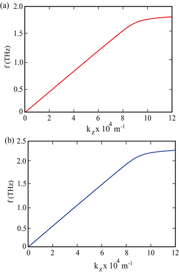
Fig. 3: Variation of frequency vs. wave number of THz surface plasmons propagating through parallel plate waveguide for Si with carrier concentration (a)  and (b)
  . The other parameters are
  ,
,  and
and  .
.
Download figure:
Standard imageModal analysis of the terahertz modes in double metal configuration
So far we have discussed dispersion properties of the terahertz surface plasmon modes supported by the waveguide. The fundamental mode, TEM or TM0 is the most dominant mode in this waveguide geometry. But along with the fundamental mode, other higher modes, i.e., TM1, TM2 and so on also propagate in the waveguide. They are rarely observed due to the lower intensity which results from higher loss offered by the waveguide structure to these modes. These modes can be identified from their cut off frequencies. For a rectangular cavity, the expression for cut-off frequency is given by

where  is the relative permittivity of the material filled inside the cavity; a is the lateral dimension and b is the width of the waveguide; m and n have integer values and represent the number of half-wavelength variations along the two transverse directions. As the one side boundary is absent in the proposed configuration, thus a is assumed to be infinite (for calculating cut-off frequency) in this type of configuration. Also
  for vacuum. Thus, the expression for the cut-off frequency of the n-th mode of the proposed structure is given by

First, we analyse the mode propagation and its field profiles in the proposed structure. We consider that the plates are made up of InSb and silicon, having a carrier concentration of  which directly determines the conductivity of the semiconductor. The dimensions of the plates are assumed to be
  in length, width and thickness, respectively. The separation between the plates is taken to be 0.5 and 0.3 mm filled with vacuum. We excited the waveguide from one end with a discrete source of broadband Gaussian pulse of frequency ranging between 0.1 THz and 1.2 THz. The transverse magnetic modes in the waveguide are excited by the input wave polarised perpendicularly to the plane containing semiconductor plates. The THz wave propagates in the vacuum region sandwiched by the two parallel plates. Figure 4 shows the electric field profile of the propagating modes.
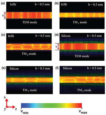
Fig. 4: The field profiles of the fundamental  ) and the higher-order modes, i.e.,
  ) and
) and  ) in the waveguide having parallel semiconducting plates of InSb and silicon.
Download figure:
Standard imageIn the electric field profiles, it may be noted that the field largely propagates in the vacuum region of the proposes structure. The amplitude of the mode decreases as we move away from the interface in the semiconductor. Figures 4(a) and (d) show the electric field profiles of the  mode in the InSb and silicon waveguides, respectively. In fig. 4(b) and (e), the fields have a cosine behaviour along the x-axis with one half-wavelength variation, thus showing the higher-order mode, i.e., TM1 in the InSb and silicon waveguides, respectively. Figures 4(c) and (f) show TM2 mode with field profile of cosine behaviour having two half-wavelength variations for the geometry. We observed that for
  only, the TEM and TM2 mode of SPPs are excited. In order to excite TM1 mode, we decreased the air gap to
  as shown in fig. 4(b) and (f). Also, when the InSb and silicon simulations are compared, the electric field penetrates more deeply in silicon compared to the InSb. This penetration of electric field of SPP in the semiconductor, which is called evanescent field, is measured in terms of skin depth. The skin depth is inversely related to the magnitude of the imaginary part of wave vector perpendicular to the interface, i.e., kx
, which is further directly proportional to the conductivity of semiconductor. InSb with higher conductivity than silicon at the same carrier concentration has higher value of imaginary part of kx
and thus exhibits lower skin depth.
as shown in fig. 4(b) and (f). Also, when the InSb and silicon simulations are compared, the electric field penetrates more deeply in silicon compared to the InSb. This penetration of electric field of SPP in the semiconductor, which is called evanescent field, is measured in terms of skin depth. The skin depth is inversely related to the magnitude of the imaginary part of wave vector perpendicular to the interface, i.e., kx
, which is further directly proportional to the conductivity of semiconductor. InSb with higher conductivity than silicon at the same carrier concentration has higher value of imaginary part of kx
and thus exhibits lower skin depth.
Comparison of the proposed waveguide with other waveguides
Next, we have compared the transmission spectra of our proposed structure with the planar plasmonic waveguide made up of InSb and metallic PPWG and the comparison is shown in table 1. We have measured the amplitude of electric field along the length of the waveguides and then fitted the data exponentially. The results are shown in fig. 5(a). It is found that the attenuation constant of the double layered plasmonic waveguide proposed in this paper is less than that of the planar plasmonic structure. The value of attenuation coefficient is  for the planar plasmonic waveguide and is
  for the proposed waveguide and PPWG. Thus loss is reduced by 30% in the double layered plasmonic waveguide as compared to planar plasmonic waveguide. We have also compared the horizontal confinement of electric field of our proposed structure with traditional parallel plate waveguide and the FWHM is calculated for the data collected in the middle of the waveguide along the propagation direction. The calculated FWHMs are shown in fig. 5(b). It is found that the FWHM of the proposed structure is 4.6 mm. It is observed that the FWHM calculated for planar plasmonic structure and metallic PPWG used for terahertz propagation are 6.2 mm and 7.3 mm, respectively. The improvement of confinement of 26% and 36% in the proposed waveguide as compared to planar plasmonic structure and metallic PPWG is attributed to the role of surface plasmons [4].
Table 1:. Comparison of attenuation coefficient  and FWHM of different waveguide structures.
| Type of waveguide | FWHM (mm) |
μ (mm
|
|---|---|---|
| Metallic PPWG | 7.3 | 0.09 |
| Planar Plasmonic (InSb) | 6.2 | 0.13 |
| Proposed waveguide (InSb) | 4.6 | 0.09 |
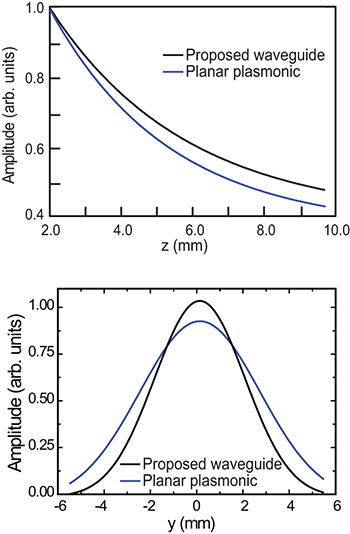
Fig. 5: (a) Transmission amplitude for the proposed structure and for planar plasmonic structure by data collected along the propagation length. (b) Comparison of confinement of field along the width of plates for the proposed structure and planar plasmonic structure.
Download figure:
Standard imageEffect of tapering on waveguide transmission
Further, we investigate broadband terahertz wave propagation through the semiconducting parallel plates of silicon with dopant concentration  . For our study, we have varied the tapering angle as
  , 1, 2, 3, 4 degrees, where 0 degrees correspond to no tapering, i.e., the output width is the same as the input width and is fixed as 0.5 mm. For simulations, we used finite element time domain solver. We considered two waveguide ports to obtain the transmission spectra: one as the source of terahertz at the untapered end, while the other as the terahertz detector at the tapered end. We have measured the integrated value of the electric field and normalized the transmission output with respect to the incident terahertz signal. The ratio of amplitudes of the transmitted and incident waves is calculated considering waveguide ports at the end of the waveguide in the
  plane in the finite element time domain solver.
The results of transmission spectra of propagation of broadband terahertz wave through the waveguide for varying output width, hence the increasing tapering angle, are shown in fig. 6(a). It can be observed from the figure that the waveguide transmission of the TM mode of the broadband terahertz wave increases as we increase the tapering angle. This indicates strong concentration of terahertz wave with the tapering of the waveguide. Next, we study the relative change in transmission amplitude with respect to the varying tapering angle, which is shown in fig. 6(b). One may notice that there is an exponential increase in the transmission amplitude when the semiconducting waveguide switched from untapered to the tapered one.
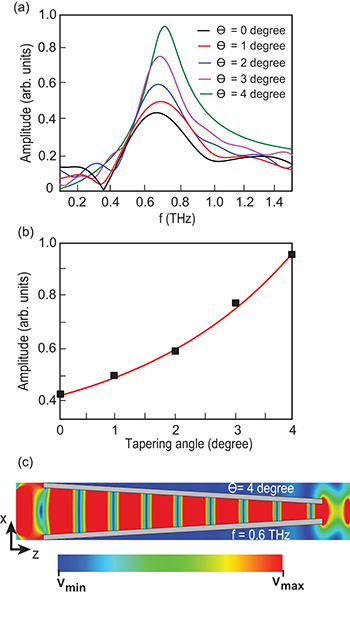
Fig. 6: Terahertz transmission through the semiconducting tapered parallel plate waveguide. Panel (a) shows transmission spectra of broadband THz wave for varying tapering angle, panel (b) shows the exponential increase in the relative change of the transmission amplitude with respect to the increasing tapering angle, panel (c) shows the electric field profile of TM mode in  plane at tapering angle
  degrees.
Download figure:
Standard imageTo have an idea of the concentration of the terahertz signal in the tapered waveguide configuration, we examined the electric field profiles of the TM mode for the waveguide tapered at  degrees at frequency 0.6 THz. The field profile in the
  plane of the waveguide is shown in fig. 6(c). It can be noticed that the tapering of the waveguide causes the terahertz signal to concentrate at the output end of the semiconducting waveguide which can be significant to a variety of applications including sensing, imaging and many others.
Conclusions
In conclusion, we have analysed the terahertz wave propagation in a thin vacuum region sandwiched by the two parallel semiconducting plates. For the incident TM polarized wave, the configuration supports surface plasmon wave with finite electric field in the vertical and the longitudinal directions. We develop an analytical formalism to obtain the dispersion relations of the surface plasmon wave at terahertz frequencies. In our analysis of dispersion properties, we observed that the saturation frequency of THz SPPs can be altered with the carrier density of the semiconductors. As we increase carrier concentration of the semiconducting plates, the saturation frequency gets blue shifted. Through numerical simulations, we investigate modal properties of the fundamental as well as higher-order modes supported by the proposed waveguide structure. The proposed structure has shown the 31% reduction of loss and 26% improvement of confinement as compared to planar plasmonic waveguides. Also the confinement is found to be improved by 37% as compared to metallic PPWG. We have also examined the terahertz propagation in the tapered semiconducting parallel plate waveguide configuring. The tapering causes strong field confinement and concentration of terahertz field at the other end of the waveguide. The waveguide transmission indicates an exponential increase in the relative amplitude with the increasing tapering angle. The present study could be significant in devising semiconductor-based communication systems utilizing parallel plate structures.
Acknowledgments
GK would like to acknowledge the financial support from Science and Engineering Research Board (SERB) (CRG/2019/002807).