

Abstract
Like their electronic counterparts, photonic integrated circuits face the challenge of further integration and miniaturization. One of the fundamental limitations comes from waveguide spacing, which leads to serious crosstalk between the neighboring waveguides when it is less than half a wavelength. Here we demonstrate a potential approach to remove this limitation and realize zero-spacing photonic waveguides with extreme compactness. This is achieved by designing pure-dielectric photonic crystal waveguides with shifted spatial dispersion and arranging them with normal dielectric waveguides alternately. Amazingly, the coupling and crosstalk between the two types of waveguides are negligible despite the zero spacing between them. Through proper designs, zero-spacing photonic bending waveguides and circuits can also be realized in practice. Such a finding opens a new avenue for ultra-compact photonic waveguides and circuits with 100% space utilization efficiency.
Export citation and abstract BibTeX RIS
Introduction
Optical waveguides, as the physical structures that guide the propagation of electromagnetic waves along designed paths, are the cornerstone of optical communication and computing. In the past century, various mechanisms of waveguide have been proposed in different scenarios. The common types of optical waveguides such as optical fibers and on-chip dielectric waveguides are mostly based on the principle of total internal reflection, where waves arriving at the interface from a high-index core to a low-index cladding are totally reflected, forming the waveguide mode confined in the core layer [1,2]. In the 1960s, the studies on surface plasmons [3,4] revealed another type of waveguides [5–9] that are composed of an interface across which the real part of the dielectric function changes sign, such as a metal-dielectric interface. The field amplitude of surface plasmon modes decays exponentially away from the interface. This method has an exceptional advantage of extreme wave confinement along the interface, but also suffers from the dissipation in metals at optical frequencies. The rise of photonic crystals (PCs) [10–17] in the 1980s brings another type of waveguide technology based on the presence of the photonic band gaps which forbid the propagation of waves within a range of frequencies. By introducing a line defect in the PC with a band gap, electromagnetic waves can propagate along the line defect, where the PCs on both sides function as wave-forbidden claddings. This method enables hollow-core waveguides and fibers at optical frequencies. Very recently, topological photonic waveguides [18–25] based on the topological edge states between a trivial and a non-trivial insulating region have attracted great interest. Such insulating regions are realized by photonic topological insulators based on PCs or metamaterials that forbid bulk wave propagation. Despite the versatile mechanisms of waveguides developed so far, claddings or wave-forbidden layers are generally indispensable. Such claddings or wave-forbidden layers cannot propagate waves in themselves, therefore the space occupied by them cannot be used to transmit signals and in a sense, it is "wasted".
For decades, there has been no doubt on the necessity of claddings or wave-forbidden layers in waveguides, as the concept is "intuitively" consistent with people's life experience. For example, walls must be used to build a maze; a river must be built with a levee; in electronic devices, conductive elements are surrounded by insulating materials. It is natural to extend the picture into the paradigm of photonic waveguiding. However, in fact, this understanding is not correct. This is because waves are different from substances like people, water and electrons, and they can be blocked in unusual ways that go far beyond the intuition in daily lives.
In our recent work and highlights [26–28], a unique approach is demonstrated to transform the wave-forbidding cladding layers into new waveguide channels with equal frequency contours (EFCs) shifted away from the EFCs of normal channels, bestowing zero coupling between them. By arranging the shifted-EFC channels and normal channels alternately, zero-spacing photonic waveguides without crosstalk can be realized. In this way, photonic waveguides shed their claddings, which opens a gate towards unprecedented waveguide systems of extreme compactness and 100% space utilization efficiency.
Previous endeavors to reduce the spacing between neighboring waveguides
Previously, great endeavors have been made to reduce the spacing between adjacent waveguides. Jahani et al. [29,30] proposed a way to relax the condition of total internal reflection to  , where n1 is the refractive index of the core, and
  is the permittivity of cladding perpendicular to the propagation direction. By introducing anisotropy in the cladding, the evanescent wave decay constant for transverse electric (TE)-polarized (electric field in plane) waves can be characterized as
  . Therefore, the larger the
  , the faster the evanescent wave decays, thus significantly reducing the spacing between the waveguides. Based on the idea of tuning anisotropy in the cladding, Mia et al. [31] further engineered the effective refractive indices of symmetric (ns
) and antisymmetric (na
) modes to achieve extremely low crosstalk between the neighboring waveguides. When
, the faster the evanescent wave decays, thus significantly reducing the spacing between the waveguides. Based on the idea of tuning anisotropy in the cladding, Mia et al. [31] further engineered the effective refractive indices of symmetric (ns
) and antisymmetric (na
) modes to achieve extremely low crosstalk between the neighboring waveguides. When  , the coupling length
  tends to infinity, where
  is the wavelength in free space. Interestingly, Song et al. and Gatdula et al. [32,33] discovered a way to reduce the crosstalk by engineering the propagation constant difference
  between adjacent waveguides. The maximum crosstalk from one waveguide to another is given by
 ![$P_{1\rightarrow 2}/P_{1}=1/[\left(\Delta \beta /2\kappa \right)^{2}+1]$](https://content.cld.iop.org/journals/0295-5075/141/1/15001/revision2/epl22100724ieqn9.gif) , where κ is the coupling strength. The crosstalk is thus low when the difference in propagation constant phase is large
, where κ is the coupling strength. The crosstalk is thus low when the difference in propagation constant phase is large  . Meanwhile, the inverse design [34,35] is also an effective approach to mitigate the crosstalk between neighboring waveguides. Despite the great progress achieved so far, the spacing between waveguides is generally larger than
  . Therefore, both academia and industry are still waiting for a practical route to further reduce the spacing between waveguides into the deep-subwavelength regime, which in principle could enormously boost dense on-chip integration.
Principles of zero-spacing photonic waveguides
The mechanisms of waveguide systems can be generally understood from the perspective of EFCs and the conservation of  at the interface. For conventional waveguide based on total internal reflection, the EFCs of core and cladding are demonstrated in red and grey lines in fig. 1(a). If the propagating waves in the core has
  (dashed line), they are evanescent in the cladding and thus form waveguide modes in the core. However, the propagating waves in cladding have
  and can always couple to the waves in the core, thus they cannot form any waveguide modes in the cladding. For the PC bandgap waveguides in fig. 1(b), there is no propagating waves in the PC at the frequency in bandgap. Thus waveguide modes are only formed in the core. Now, imagine that there are two types of waveguides whose EFCs are separated in the direction of the waveguides, i.e., kx
. Due to mismatched kx
, the propagating waves in the two types of waveguides cannot couple to each other when their interface is also along the x-direction. As a result, independent waveguide modes can be formed in both waveguides, and the crosstalk between them is negligible even though the two waveguides have zero spacing, as shown in fig. 1(c). The next question is: how to realize materials with shifted EFCs?
and can always couple to the waves in the core, thus they cannot form any waveguide modes in the cladding. For the PC bandgap waveguides in fig. 1(b), there is no propagating waves in the PC at the frequency in bandgap. Thus waveguide modes are only formed in the core. Now, imagine that there are two types of waveguides whose EFCs are separated in the direction of the waveguides, i.e., kx
. Due to mismatched kx
, the propagating waves in the two types of waveguides cannot couple to each other when their interface is also along the x-direction. As a result, independent waveguide modes can be formed in both waveguides, and the crosstalk between them is negligible even though the two waveguides have zero spacing, as shown in fig. 1(c). The next question is: how to realize materials with shifted EFCs?

Fig. 1: The mechanisms of the conventional waveguide, PC waveguide and zero-spacing photonic waveguides from the perspective of EFCs. (a) Conventional waveguide. The EFCs of the core and cladding are in red and grey lines. Waves with kx greater than the dashed line form the waveguide mode in the core. (b) PC waveguide. The EFC is absent for the PC due to the band gap. Waves in the core as a line defect formed the waveguide mode. (c) Zero-spacing photonic waveguides composed of channels with shifted EFC and normal channels. The EFC of the shifted-EFC channel is outside the dashed line, while the EFC of normal channel is within the dashed line. Waves in both channels can form independent waveguide modes without any crosstalk.
Download figure:
Standard imageThis issue of shifting EFCs has actually been discussed for a long time in the topic of effective gauge potentials [36–45]. For instance, the authors of [36–39] considered a resonator lattice in which the coupling constants between the resonators are harmonically modulated in time. By introducing the special phase of the modulation between the nearest resonators, they found that the EFC can be shifted effectively. Chen et al. [40] proposed a new type of wire metamaterial possessing one or more index ellipsoids centered at nonzero k -points, with linear bands that go to zero frequency at some k ≠ 0. The existence of the quasistatic modes at nonzero k -points can be viewed as the shifting of the light cone by a synthetic gauge potential induced by the twisting in network. The authors of [44,45] found that the dispersion relations in the core and the cladding can be shifted from one another in momentum space, by using waveguide arrays with non-trivial trajectories, i.e., using different tilted arrays in the core and cladding. Liu et al. [41–43] proposed an approach to obtain effective gauge field in real space for photon propagation using reciprocal anisotropic media, based on which the photonic Aharonov-Bohm effect is observed.
Interestingly, besides the effective gauge potential, dielectric PCs also provide a convenient and low-loss approach to realize shifted EFCs, which shall be elaborated in the following.
Realization of shifted EFC by PC and omnidirectional impedance matching
In the studies of PCs [46–48] it is known that EFCs in the second/high band of general PCs can be shifted to be centered at the X point at the Brillouin zone edge. Interestingly, omnidirectional (0–90°) impedance matching with free space can be obtained for the PCs with shifted EFCs, through the engineering of the unit cell. Figure 2 shows the first example that was reported, although it was later found that the structure could be greatly simplified. The engineered unit cell is illustrated in fig. 2(a), and the corresponding band structure and EFC are shown in figs. 2(b) and (c), respectively. The height (i.e., the maximum  ) of PCs EFC is adjusted to be the same as the EFC of free space, which is found to be crucial for perfect impedance matching at large incident angles. From the diagram of the impedance difference of the PC and free space of the third band in fig. 2(d), we see that the impedance difference is very small for almost all ky
< k0 at the working frequency fa/c = 0.3183 (dashed line in fig. 2(b)), indicating the omnidirectional impedance matching with free space. A numerical verification is presented in fig. 2(e), where the transmittance through the PC slab consisting of N (=4, 5, 6, 15) layers of unit cells in the x-direction is found to be near unity (∼99%) for nearly all incident angles, and is almost irrespective of the layer number N. Therefore, such a PC structure allows free-space propagating waves to enter without inducing any reflections, irrespective of the incident angle and the shape of the incident wavefront.
) of PCs EFC is adjusted to be the same as the EFC of free space, which is found to be crucial for perfect impedance matching at large incident angles. From the diagram of the impedance difference of the PC and free space of the third band in fig. 2(d), we see that the impedance difference is very small for almost all ky
< k0 at the working frequency fa/c = 0.3183 (dashed line in fig. 2(b)), indicating the omnidirectional impedance matching with free space. A numerical verification is presented in fig. 2(e), where the transmittance through the PC slab consisting of N (=4, 5, 6, 15) layers of unit cells in the x-direction is found to be near unity (∼99%) for nearly all incident angles, and is almost irrespective of the layer number N. Therefore, such a PC structure allows free-space propagating waves to enter without inducing any reflections, irrespective of the incident angle and the shape of the incident wavefront.

Fig. 2: The PC with shifted EFC and omnidirectional impedance matching. (a) Schematic diagram of PC unit cell. (b) The band structure of the PhC. (c) The EFC of the third band. (d) The impedance difference of the PhC and free space of the third band. (e) Simulated transmittance through the PhC slab with N (= 4, 5, 6, 15) layers of unit cells as a function of the incident angle.
Download figure:
Standard imageThe PC with shifted EFC and omnidirectional impedance matching provides excellent platforms for realizing all-dielectric illusion optics [49], omnidirectional perfect absorbers [50], etc. The principle is universal and has been extensively investigated in THz frequencies [48] and in acoustics [51,52], based on which a wide-angle broadband non-reflecting acoustic fence was experimentally demonstrated [52].
The omnidirectional impedance matching effect brings the significant advantage of high-efficiency coupling into the waveguide and helps to eliminate the backscattering from the interconnects between PC and free space channels around the bending, thereby mitigating the unnecessary bending losses. We also note that full-angle impedance matching is not required for lower-order waveguide modes, especially the fundamental mode. Therefore, we choose the PC structure to realize the shifted EFC required in the shifted-EFC channel.
Demonstration of zero-spacing photonic waveguide circuits
A simplified example of the PC with shifted EFC and wide-angle impedance matching is shown in fig. 3. The unit cell of group symmetry of  is shown in fig. 3(a). Here, a is the lattice constant and b = 0.6a. The background is free space
  , and the dielectric rods have a permittivity
  . The band structure for transverse-magnetic (TM) polarization (electric field in the z-axis) is calculated and shown in the lower panel of fig. 3(a). At a working frequency fa/c = 0.2962 (dashed line), the EFC is shown as the red lines in fig. 3(b). The dotted box represents the boundary of the first Brillouin zone, and the black lines denote the circular EFC of free space. Obviously, this PC has met the requirement of the shifted EFC channel in fig. 1(c).
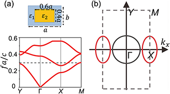
Fig. 3: Schematic diagram of PC with shifted EFC. (a) The unit cell of this PC and its band structure for TM polarization. The dashed line marks the working frequency. (b) The EFCs of PC (red lines) and free space (black line). The dotted box represents the first Brillouin zone.
Download figure:
Standard imageThe theory has been verified by microwave experiments, as plotted in fig. 4. A zero-spacing waveguide array is constructed by arranging the PC channels with shifted EFCs and free-space channel alternately. We note that the propagation constants in the free-space and PC channels, i.e.,  and
and  , always have
  and
and  , respectively, where k0 is the wave number in free space. The crosstalk between the two channels is thus inherently minimized. The schematic diagram of the waveguide array is demonstrated in fig. 4(a). The dielectric rods have
  , and the unit cell is of a = 6 mm and b = 3.6 mm. The working frequency is around 15 GHz. The waveguide array is designed as four PC waveguides (A1−4) and four free-space waveguides (B1−4) with different widths of
  , which confirms the arbitrariness of the width w. An additional PC layer with
  is placed beside the B4 free-space waveguide for confinement. We excite the eight channels one by one from their left ports. Here, we show the results by exciting A2, B2, A4 and B4 waveguides in fig. 4(b). From the field intensity distributions, we find that each waveguide channel can transmit waves independently, without coupling to waves in other channels. This suggests that the crosstalk between the adjacent channels is negligible, despite the zero spacing. We note that both types of channels in zero-spacing waveguides have fundamental and higher-order modes, and the field distributions are similar to the waveguide modes of the present waveguide. This indicates relatively high coupling efficiency due to mode matching.

Fig. 4: The zero-spacing photonic waveguides without crosstalk. (a) The photo of a waveguide array consisting of four PC channels ( ) and four free-space channels (
 ) with different widths of
  . (b) The simulated intensity patterns of A2, B2, A4 and B4 channels by only exciting the corresponding input port. (c) The photo of a zero-spacing bending waveguide array and a zero-spacing photonic circuit. The input and out ports are denoted by Ii
(i = 1, 2, 3, 4) and Oi
(i = 1, 2, 3, 4), respectively. (d) The field intensity distributions of the zero-spacing bending waveguides and photonic circuit by exciting the input ports Ii
(i = 1–4).
. (b) The simulated intensity patterns of A2, B2, A4 and B4 channels by only exciting the corresponding input port. (c) The photo of a zero-spacing bending waveguide array and a zero-spacing photonic circuit. The input and out ports are denoted by Ii
(i = 1, 2, 3, 4) and Oi
(i = 1, 2, 3, 4), respectively. (d) The field intensity distributions of the zero-spacing bending waveguides and photonic circuit by exciting the input ports Ii
(i = 1–4).
Download figure:
Standard imageAmazingly, sharp-bending waveguides with zero spacing can also be constructed via this scheme [15,53]. Figure 4(c) demonstrates the experimental setup of a zero-spacing sharp-bending (90°) waveguide array and a zero-spacing photonic circuit in which the waves are routed around to traverse the entire physical space of the circuit. High-efficiency sharp bending can be realized by engineering the corner unit of bending waveguides. In the sharp-bending array shown in fig. 4(c), the input and output ports of the three transmission channels are denoted by Ii and Oi (i =1, 2, 3), respectively. The input ports are excited separately, and the intensity patterns are plotted in the three left panels of fig. 4(d). The results indicate high-efficiency bending with zero spacing is realized. A 180° bend can be realized via two successive 90° bends and a photonic circuit in which waves traverse the entire physical space can be realized by applying a series of the 90° and 180° bends. In the right panel of fig. 4(c), we demonstrate a photonic circuit composed of two 180° bends and one 90° bend. The input and out ports are denoted by I4 and O4, respectively. From the result of intensity pattern shown in the right panel of fig. 4(d), it is clearly seen that high-efficiency routing with zero spacing is realized.
The theory of zero-spacing photonic waveguides without crosstalk can be easily extended to the optical regime. In our recent work [26], we also find that the zero-spacing photonic waveguides composed of silica and silicon are available around 1550 nm. And the separation between the central axes of adjacent channels can be smaller than half a wavelength. Furthermore, we note that the working bandwidth of the zero-spacing photonic waveguides is >130 nm, which is sufficient for practical optical chips.
Conclusions and perspectives
From the perspective of momentum, the physical origin of zero-spacing photonic waveguides without crosstalk lies in the introduction of a dispersion shift in the momentum space. It should be emphasized that such a shift does not impose any limitation on the propagating direction of the waves, because the propagating direction is determined by the group velocity, which is normal to the elliptical EFC and can be pointed in any direction. In fact, both the waves in free space and the PC with shifted EFC can propagate along any directions, but amazingly, they will be totally reflected at the interface between free space and the PC due to the mismatched momentum. In this sense, such an interface functions like an artificial "virtual reflecting boundary" of zero thickness. Such a phenomenon is a unique characteristic of waves.
The establishment of two media with spatial dispersions and EFCs shifted away from each other enables zero-spacing waveguide systems that were previously impossible. This breakthrough directly shrinks the spacing between neighboring waveguide channels to absolute zero, without inducing any crosstalk. In other words, a "maze" (circuit) for photons is realized without using "walls" (claddings). From another perspective, this approach blurs the distinction between the cores and claddings in previous waveguide systems. This principle is universal and can apply to general types of waves, such as microwaves, THz waves, optics and acoustics.
Acknowledgments
The authors acknowledge financial support from the National Key Research and Development Program of China (2020YFA0211300 and 2017YFA0303702), the National Natural Science Foundation of China (Grant Nos. 12174188, 11974176, 11634005, 11974177, and 61975078) and Postgraduate Research & Practice Innovation Program of Jiangsu Province.
Data availability statement: The data that support the findings of this study are available upon reasonable request from the authors.