
Abstract
To obtain an engineered surface for deposition of high-Tc superconductors, nanoscale modulations of the surface of the underlying LaMnO3 (LMO) cap layer is a potential source for generating microstructural defects in YBa2Cu3O7−δ (YBCO) films. These defects may improve the flux pinning and consequently increase the critical current density, Jc. To provide such nanoscale modulation via a practical and scalable process, palladium (Pd) or tantalum (Ta) nano-islands were deposited using dc-magnetron sputtering on the surface of the cap layer of commercial metal tape templates for second-generation wires. The size and density of these nano-islands can be controlled by changing sputtering conditions such as the power and deposition time. Compared to the reference sample grown on an untreated LMO cap layer, the YBCO films grown on the LMO cap layers with Pd or Ta nano-islands exhibited improved in-field Jc performance. Atomic force microscopy and transmission electron microscopy were used to assess the evolving size and density of the nano-islands.
Export citation and abstract BibTeX RIS
Corrections were made to this article on 25 January 2012. Amendment to an affiliation was made.
1. Introduction
Wide ranging usage of high temperature superconductors (HTS) in several electric power applications such as motors, generators, and underground transmission cables requires HTS wires capable of conducting high density critical currents at high temperatures in the presence of magnetic fields. For operation in such power utility applications, the ability to immobilize the quantized magnetic flux lines—vortices—in the high temperature superconducting material must be improved through nanoscale material defects. Although HTS materials contain native defects such as oxygen/cation vacancies, dislocations, etc, that act as pinning centers, it has been shown that the artificial introduction of pinning centers plays a crucial role in further improving the critical current density Jc in high magnetic fields and at high temperatures [1–3]. In particular, numerous studies during the last decade have introduced a variety of artificial pinning defects into HTS films through nanostructural engineering [4–17]. In addition to the usual approaches of directly forming pinning centers in the HTS with second phase precipitates or irradiation damage, a complementary approach has been to deposit the HTS onto nanostructurally modified substrate surfaces. For example, through modification of LaMnO3 (LMO) buffer layers by co-deposition with MgO we were able to create chemically phase-separated and structurally self-assembled MgO nanocolumns within the LMO matrix [18]. The YBa2Cu3O7−δ (YBCO) films deposited on these nanostructured cap layers showed enhanced in-field Jc properties due to defects generated in the YBCO matrix, associated with growth on the phase-separated MgO nanocolumns. In another example, cap layers comprising phase-separated BaTiO3–CoFe2O4 have been synthesized with various densities and surface structures, leading to improved flux pinning in the YBCO coatings [19].
It has also been demonstrated that decorating the substrate surface with a variety of nanoparticles prior to HTS film deposition is an effective and practical method to introduce additional flux pinning centers into YBCO films [20–24]. An advantage of surface decoration is that a variety of nanoparticles can be applied on various substrates using simple and scalable methods, such as chemical solution and physical vapor deposition methods, while not poisoning or producing other deleterious effects on the overlying YBCO. Recently, Sarkar et al have shown that the critical current density of thick (>1 μm) YBCO films on SrTiO3 substrates can be improved by a combination of substrate surface decoration and quasi-superlattice approaches employing Pd nanodots between YBCO layers deposited by pulsed laser deposition (PLD) [25, 26]. Based on the observed positive effects of Pd on the flux pinning performance of YBCO films, as well as the generally established groundwork of nanoparticle substrate surface decoration, we have extended our studies to technological substrates used for fabrication of coated conductors, utilizing a high-rate method—sputtering—to form the nano-islands. In the present work, the surface of commercial LMO-buffered ion beam assisted deposited (IBAD) substrates was decorated with palladium (Pd) or tantalum (Ta) nano-islands, prior to YBCO film growth, using dc-magnetron sputtering, which is a far more scalable method than PLD. We have also demonstrated that the density and size of the nano-islands can be varied by the deposition conditions, such as deposition temperature, power, and time, as well as by post-annealing procedures. To establish that these surface-decorated LMO buffer layers indeed produce enhanced flux pinning in subsequent HTS layers with no deleterious side effects, we deposited 0.8 μm thick YBCO films using PLD methods and investigated their transport current properties.
2. Experimental aspects
The Pd or Ta nano-islands were deposited by dc-magnetron sputtering on LMO/homo-epitaxial MgO/IBAD-MgO/Hastelloy templates (LMO-IBAD substrates). The LMO-IBAD substrates used in this study were fabricated by SuperPower, Inc. (Schenectady, NY, USA) [27]. Metallic Pd or Ta sputter targets of diameter 2 inch were used. Depositions were carried out in Ar and Ar + H2 gas mixtures at typical sputter gas pressures of 3 mTorr, and at a substrate temperature of 750 °C. For the Ta nano-islands, this was followed by post-annealing at 850 °C in 1 atm flowing Ar gas ambient; the Pd nano-islands were not post-annealed. The nano-islands, once formed on the LMO surface, were studied by atomic force microscopy (AFM). For this, a Digital Instruments Nanoscope III AFM was employed in contact mode.
Subsequently, 0.8 μm-thick YBCO films were deposited on the surface decorated IBAD templates by PLD using a KrF excimer laser. The energy density and repetition rate were ∼2 J cm−2 and 10 Hz, respectively. During deposition, the substrates were kept at a substrate temperature of 790 °C in an oxygen partial pressure of 300 mTorr. Heating to this temperature required approximately 25 min and the substrates were held ∼10 min at 790 °C before beginning PLD of the YBCO material, which lasted 20 min. Subsequently the system was cooled to 500 °C (in ∼12 min), where the films were annealed in 1 atm of O2 for 30 min, then furnace cooled to achieve full oxygenation.
The transport Jc measurements were conducted at 77 K using a standard four-probe method and Jc values were assigned at a 1 μV cm−1 electric field criterion. The dependence of Jc on angular orientation of the magnetic field (spanning a range of 110°) was investigated in the full Lorentz force configuration at 77 K and in a 1 T magnetic field. Cross-sectional transmission electron microscopy (TEM) was carried out to characterize the finished coated conductor containing Pd nano-islands.
3. Results and discussion
Pd and Ta nano-islands were grown at various power rates and deposition times. AFM images shown in figures 1 and 2 reveal that the dimension and density of islands strongly depend on the parameters such as deposition time, substrate temperature, and power. Some results for the formation of Pd nano-islands at different growth power rates and deposition times are shown in AFM images in figure 1. Compared with the Ta nano-islands shown in figure 2, the as-deposited Pd nanoparticles are considerably smaller. Figures 1(a) and (b) show AFM images for different deposition times at a power of 10 W. Longer deposition times produce more nanoparticles, while the size and height are nearly unchanged, around ∼30 nm and 7–15 nm, respectively. For these as-deposited materials, the number densities were measured to be ∼3 and 7 × 10¹⁰ islands cm−2 for the samples deposited for 3 and 7 s, respectively. The morphological features of islands deposited at higher sputtering power, 100 W, for deposition times of 10 and 20 s are shown in figures 1(c) and (d), respectively. In these figures, the average dimensions of the islands are similar to those deposited at 10 W power (figures 1(a) and (b)), while a higher power gives a somewhat larger area density of islands; it is clear, however, that the net amount of Pd metal deposited does not scale linearly with the input sputtering power. Average values for the sizes and densities for all materials are summarized in table 1, where the uncertainty in the quantities is estimated to be ±30%. As noted above, these Pd-decorated LMO surfaces were not post-annealed before AFM imaging. Finally, a YBCO film was deposited at 790 °C on the substrate decorated with Pd islands for 7 s, whose as-deposited surface morphology is exhibited in figure 1(b).
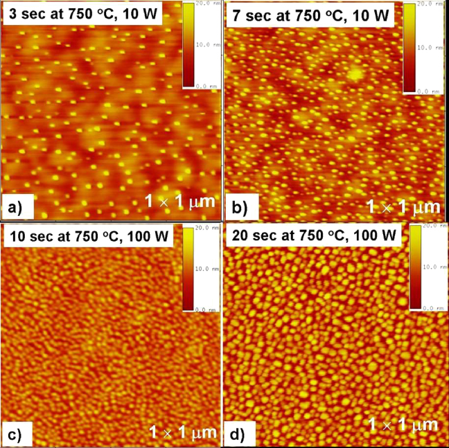
Figure 1. AFM images of Pd nano-islands sputtered onto LMO-IBAD substrates at 750 °C for the indicated deposition times and powers. The size and density of islands can be tuned by varying the deposition conditions.
Download figure:
Standard image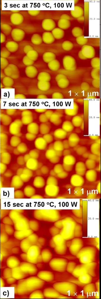
Figure 2. AFM images of Ta nano-islands on LMO-IBAD substrates after deposition times of (a) 3 s, (b) 7 s, and (c) 15 s. These materials were post-annealed at 850 °C before imaging.
Download figure:
Standard imageTable 1. Approximate area density and dimensions of nano-islands as-deposited by sputtering onto LaMnO3 buffer layers at 750 °C; Ta materials were post-annealed at 850 °C before imaging, as described in the text.
| Nano-island material | Sputtering power (W) | Deposition time (s) | Density (1010 cm−2) | Diameter (nm) | Height (nm) |
|---|---|---|---|---|---|
| Ta | 100 | 3 | 0.4 | 130 | 15–20 |
| Ta | 100 | 7 | 0.6 | 130 | 35–45 |
| Ta | 100 | 15 | 0.4 | 250 | 25–30 |
| Pd | 10 | 3 | 2.3–4.0 | 30 | 7–15 |
| Pd | 10 | 7 | 7.2 | 30 | 11–12 |
| Pd | 100 | 10 | 13–15 | 20–30 | 6–10 |
| Pd | 100 | 20 | 9.0–9.4 | 35 | 11–12 |
A subsequent TEM study of the completed coated conductor gave evidence for significant redistribution of the Pd material during the deposition of YBCO by PLD. This is illustrated in figure 3, where a cross-sectional image shows Pd nano-islands on top of the LMO cap layer and embedded in YBCO. These particles have diameters of ∼65 nm with heights near 50–60 nm. Analysis of low magnification images (not shown) of a larger area containing more particles confirms these dimensions, and gives an average particle separation (in projection) of 170 nm. This corresponds to an area density of islands ≤0.35 × 1010 cm−2, which is a factor of 20 smaller than that observed in the sample prior to YBCO deposition. However, the accompanying coarsening of particle size (2 × in diameter and 5 × in height) means that the average Pd mass per unit area is conserved. This island growth and mass redistribution may arise from an enhanced surface mobility due to impingement of energetic, epithermal material in the laser plume, perhaps coupled with the presence of oxygen during the PLD process and the higher substrate temperature. Elemental analysis of the Pd-based nano-islands by energy dispersive x-ray (EDX) methods showed them to be metallic in nature rather than Pd-oxide, as evidenced by dominant Pd peaks accompanied by weak Cu, Ba, Y and O peaks from the surrounding YBCO matrix. At the PLD deposition temperature and oxygen partial pressure, metallic Pd is the equilibrium phase [28, 29]; the observed presence of metallic Pd in the completed films suggests that a combination of sluggish kinetics with the buried nanoparticles inhibits whatever tendency they may have to oxidize during cooling to room temperature.
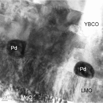
Figure 3. A cross-sectional TEM image of a YBCO film deposited on an LMO surface, which was decorated with Pd nano-islands sputtered for 7 s at 750 °C and 10 W. Stacking faults, lying approximately parallel to the LMO surface, are visible in the YBCO material.
Download figure:
Standard imageFigure 2 shows images of Ta nano-islands deposited on LMO-IBAD substrates at 750 °C with 100 W power. These substrates were immediately post-annealed at 850 °C in a 1 atm Ar gas ambient for 30 min, prior to AFM imaging. Sputtering times of 3, 7 and 15 s were used for figures 2(a)–(c), respectively. As can be seen from these figures, the density and dimension of the islands vary with deposition time. The lateral size of the islands grown at 3 and 7 s range from 100 to 130 nm and their height is ∼15–45 nm. On the other hand, a longer deposition time of 15 s increased the size of the Ta nano-islands to ∼250 nm, while their heights were similar, near ∼25–30 nm. In all these cases, the areal density of islands was approximately 0.5 × 1010 cm−2. When the sputtering time further increases, islands start to coalesce and cover the film surface. It is important to note that post-annealing or deposition at high temperatures provides more kinetic energy and increases the effective mobility of small clusters on the surface, thereby promoting the formation of larger clusters in a manner similar to the Ostwald mechanism [30]. A HTS YBCO film was grown on the Ta nano-islands deposited for 3 s, the surface topography of which is shown in figure 2(a).
Superconducting transition temperatures Tc ≈ 88–89 K were observed for the YBCO films on the LMO cap layers decorated with Pd or Ta nano-islands. The Tc of the control sample was the same, meaning that the presence of the nano-islands produced no adverse effects such as poisoning of the YBCO layer. The dependence of the critical current density Jc on magnetic field and its orientation is shown in figure 4. Results are presented for 0.8 μm thick PLD YBCO films, deposited on LMO-IBAD substrates decorated with Pd or Ta nano-islands, and these data are compared with a control sample that was similarly deposited on an untreated LMO surface. For all samples, these transport measurements revealed a Jc in self-field, Jc (s.f., 77 K) of ≈ 2.7 MA cm−2. Figure 4(a) compares the dependence of Jc (77 K) on magnetic field (where the field is applied parallel to the c-axis) for a YBCO film on Pd-decorated LMO with that for a typical YBCO film similarly deposited on an LMO-capped substrate without surface decoration. While the two superconducting materials have similar superconducting transition temperatures and similar Jcs in self-field, the Pd-decorated sample is superior in-field. Indeed, the relative improvement becomes progressively more significant in larger magnetic fields, indicating enhanced pinning. In coated conductors, a power-law falloff of the form Jc ∝ H−α is often observed at intermediate field levels. The power-law index α (as deduced from the slope of log–log plots of Jc(H)) has values of 0.49 and 0.45 for the standard YBCO and YBCO on Pd-decorated LMO substrates, respectively. These results confirm the visual impression that the film on the surface-decorated sample shows less field dependence than the film on the standard LMO cap layer. Thus, figure 4(a) clearly demonstrates that YBCO on a surface-engineered LMO substrate exhibits significantly improved Jc compared to that obtained for the standard counterpart. Unfortunately, no corresponding data are available for YBCO on the Ta-decorated surface (shown in figure 2(a)) as it was burned out during the measurements described next. We now consider for all three substrates the dependence of Jc on orientation of an applied magnetic field.
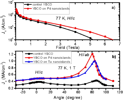
Figure 4. Transport critical current density of 0.8 μm thick YBCO films on Ta- or Pd-decorated LMO cap layers. (a) In-field performance at 77 K with magnetic field applied parallel to the tape normal (nearly ∥ to the c-axis) and (b) dependence of critical current density at 1 T and 77 K on orientation of the applied magnetic field, relative to the film's normal direction. The data are compared with a similarly prepared YBCO film on an LMO cap layer without any surface decoration.
Download figure:
Standard imageThe variation of Jc with magnetic field orientation gives valuable information regarding the nature of vortex pinning in the material. This angular dependence of Jc at 77 K in a magnetic field of 1 T is shown in figure 4(b). The angle θ is defined as the angle between the applied field and the normal to the plane of the superconductor. Data presented in figure 4(b) reveal significant improvement in Jc for all orientations of the field. In particular, the YBCO films on surface decorated substrates show a significantly larger peak for H near the ab-plane (θ = 90°), compared with the peak for the reference YBCO/LMO sample. As can be seen in figure 4(b), the peaks are offset from θ = 90° for all these materials. This is a consequence of the fact that coated conductor materials on IBAD templates commonly display some tilting of the buffer and HTS lattice planes and defect structures relative to the substrate. This produces peaks in Jc when the magnetic field is applied near but not quite parallel to the sample surface, as discussed by Holesinger et al [31] and Zhang et al [32]; hence the pronounced peaks at θ = 80°–85°can be attributed to similar correlated disorder near the ab-planes. In general, such disorder includes stacking faults, layering of the precipitates, and intergrowths [17, 33–35]; additional contributions may come from dislocation cores at the low-angle grain boundaries and/or other naturally occurring ab-plane aligned defects that are related to the growth process of YBCO [36–38]. Indeed, figure 3 shows the presence of stacking faults, which have been strongly correlated with enhanced ab-plane pinning [17] in PLD films of (Y–Sm)BCO. Also, stacking faults contribute markedly to the prominent ab-plane peaks observed in coated conductors produced differently, e.g. by metal organic deposition (MOD) processing [39]. Finally, Y2O3 and Cu-oxide materials, layered approximately parallel to the substrate surface, were observed by low resolution TEM. The significant pinning near the ab-plane in the present materials most likely arises from a combined action of these vortex pinning defects.
When the magnetic field is oriented near the c-axis, a much broader and barely visible peak in Jc is obtained. Such a peak generally arises from some form of correlated disorder along the c-axis, such as naturally occurring threading dislocations, twin boundaries, and grain boundary dislocations, or artificially introduced columnar defects from energetic particle irradiation or self-organized growth. In earlier work by others on somewhat similar materials with surface-decorated Ag nanodots combined with Ag nanodots interspersed between YBCO multilayers [40], evidence was found for defects oriented along the c-axis that might provide angularly selective vortex pinning. No similar structures or defects are visible in the present materials. In fact, the c-axis peak in figure 4(b) is less prominent and suppressed in the surface-decorated materials compared with the control sample. The reason for this is unclear, but may arise from a complex interaction between the vortices and the defects additionally generated by the presence of nano-islands. Recently, it was reported that increasing the number density of stacking faults induced by Sm substitution onto Y and Ba sites leads to substantial improvement in the pinning for H ∥ ab while suppressing the pinning for H ∥ c [17]. An additional mechanism may be a reduced density of near-substrate misfit dislocations that can provide significant c-axis pinning [41], particularly for thinner HTS layers. The similarity of the angular dependences and magnitudes of Jc for the YBCO films on the LMO-IBAD substrates decorated with two different nano-islands, Pd or Ta, suggests that the contributions from correlated and uncorrelated pinning structures are comparable in the two cases. As generalized guidance for use in manufacturing of coated conductors, both decoration materials led to enhanced properties, although the Ta case has been investigated less extensively.
It is clear that surface decoration with nano-islands led to wide-ranging improvement of Jc of the YBCO films. One possible scenario is that each nanoparticle acts like a short columnar defect to pin an individual vortex. This possibility is unlikely, however, in view of the (lack of) orientational dependence; furthermore, the area density of nano-islands is low and equivalent to the density of vortices in a 'matching field' of only ∼0.1 T, while the enhancements in Jc extend to much higher fields. Alternatively, individual particles are large enough that each might accommodate several vortices in fields larger than Φ0/(particle diameter)2 ∼ 0.5 T, and their height is ∼6% of the film thickness, meaning that a significant length of vortex could be trapped. The nominally equiaxial particles would, in and of themselves, impart little dependence on the orientation of magnetic field, in keeping with the θ-insensitive experimental data in figure 4(a). Furthermore, the nonuniform, decorated interface with the YBCO may introduce strain and possibly defect structures in the matrix that act as nominally isotropic pinning centers [19, 21, 22, 41, 42]. Finally, layered defects near the ab-plane produce pronounced pinning and Jc enhancement for in-plane fields, as already noted.
4. Conclusions
In conclusion, we have nano-engineered the surface of the LMO cap layer on commercial IBAD tape templates by formation of Pd and Ta nano-islands, using readily scalable sputtering methods. It has been demonstrated that the size and density of these nano-islands can be tuned by varying the deposition conditions such as deposition temperature, power, and time; however, further processing, specifically YBCO deposition by PLD on Pd-decorated LaMnO3, led to substantial coarsening and island growth. These nano-islands induce additional disorder within the YBCO films, effectively leading to improved pinning characteristics and higher in-field Jc performance. The present study underscores that the performance of HTS films on technologically important substrates can be enhanced by employing the simple, scalable and practical route of substrate surface decoration.
Acknowledgments
The work of ÖP and JWS was supported by the Materials Sciences and Engineering Division, Office of Basic Energy Sciences, US Department of Energy. Research at ORNL (JRT, KJL, MPP, SHW, YLZ, DKC, TA) was sponsored by the US Department of Energy, Office of Electricity Delivery and Energy Reliability, Advanced Cables and Conductors.