

Abstract
We have observed evidence of superconductivity at temperatures in the vicinity of 260 K in phosphorus-doped graphite and graphene. This evidence includes transport current, magnetic susceptibility, Hall effect and (pancake) vortex state measurements. All of these measurements indicate a transition which is that of a type II superconductor with no type I phase until below the limits of our measurement capabilities. Vortex states are inferred from periodically repeated steps in the resistance versus temperature characteristics of highly oriented pyrolytic graphite and exfoliated doped multilayer graphene. Magnetic susceptibility measurements have shown results qualitatively similar to those expected (and experimentally observed by others) for ultra-thin (thickness ≪λL) films. The magnetization is negative for field-cooled and zero-field-cooled measurements. The magnetization for field cooled and zero-field-cooled measurements begin to diverge at approximately 260 K. Hall effect measurements show a sign reversal in the Hall voltage as the temperature is reduced from 300 K to 78 K.
Export citation and abstract BibTeX RIS
1. Introduction
Carbon has a large number of allotropes exhibiting different mechanical, chemical and electrical properties [1]. Recently, many researchers have turned their attention to graphene [2], a two-dimensional carbon structure that can be used as a test object to study possible electron pairing necessary for superconductivity. Highly oriented pyrolytic graphite (HOPG) can be used in this experimental study since interlayer coupling in it is weak [3, 4] and it approximates graphene fairly well. Our earlier work [5] has given every indication that there is superconductivity in doped HOPG and, possibly, in graphene as well. For this reason it was decided to extend the work to include graphene, both exfoliated from ion-implanted HOPG and doped, in situ-grown graphene as a subject of study for superconductivity.
The observations reported here do not fit any phenomenon known to us other than superconductivity. As a result, in this work, we have chosen to follow the possibility that superconductivity is present. It is important to note that we are not ruling out some new and previously undiscovered physical manifestation of the extreme anisotropy and two-dimensionality of the material, but we have found no better model than superconductivity to base any behavioural predictions on.
The rest of this paper is organized into a discussion of the relevant background upon which this work rests, the experimental methods used in the work, the results of the various experiments, and a discussion after which some general conclusions are drawn.
2. Background
It has been hypothesized by us [5] and others [6–8] that the close coupling or strong scattering of electrons by both phonons and plasmons in graphene indicates a potential for superconductivity at considerable temperatures in doped graphene [9, 10]. Kopelevich et al [11–13] reported a few cases of suspected superconductivity in HOPG but, given that the results were only on as-grown samples, the likelihood of the observations being due to superconductivity was unclear. Our prior work [5] is the first that we are aware of where a systematic attempt has been made to substitutionally dope HOPG/graphene/graphite into a superconductive state. Additional later work by Scheike et al [14, 15] and Ballestar [16] has also given hints of possible superconductivity in doped graphite. The work described herein represents our effort to attempt to confirm or disprove that these results originate superconductivity.
Moving from bulk ion-implanted HOPG to exfoliated graphene from ion-implanted HOPG allowed the removal of bulk effects from the physics occurring in the first 20 nm, where the dopant and damage from the implantation were located. The further move to the use of phosphine as a dopant in doped-while-grown plasma CVD films has minimized the implantation damage. Exfoliation, pioneered by Novoselov and Geim [2], has been used to obtain samples for measurements by a large number of other researchers. The reader is referred to a few representative references for further discussion of the various techniques used [17–19].
Prior work on doped HOPG [5] showed that the sample's resistance never went to zero, even at low temperatures. A review of the literature involving resistance measurements in layered superconductors leads to the identification of flux-flow resistance as a potential reason for the non-zero resistance at low temperatures [20, 21]. The literature indicates that flux pinning is key in reducing flux-flow resistance in layered high-TC superconductors [20–27]. If this failure of the resistance to reach zero ohms is due to vortex flow then flux pinning would likewise be important in our samples. Another point that becomes clear upon examination is that, with an exfoliated film only a nanometer or two thick, the test current in a resistance versus temperature measurement must be as small as possible or it could influence the results due to either local magnetic fields or heating.
An examination of the volume of prior work [22–29] that has been done to characterize and model the behaviour of magnetic vortices in layered superconductors leads to the conclusion that pancake vortices would be the preferred vortex form if this extremely anisotropic material (the ratio of the in-plane resistivity to the normal direction resistivity in pure multilayer graphene is greater than 100 000:1) is superconducting [30, 31]. A more specific conclusion (derived from the work by Pe, Benkraouda and Clem [24]) is that, for graphene stacks with interlayer distances of 0.2 nm and relatively long magnetic penetration depths (graphene and graphite are diamagnetic materials with significant magnetic anisotropy [32]), the interlayer coupling, if the material was a superconductor with a magnetic self-pinning attractive force, between pancake vortices in layers i and j is given as follows:
where

Λ is the 2D thin-film screening length, λ|| is the effective penetration depth parallel to the graphene planes, and s is the interlayer spacing.
Where the layers i and j are adjacent and the vortices are directly vertically aligned, this reduces to

It is obvious from this simplistic analysis that the magnetic pinning force between two pancake vortices in adjacent layers is proportional to the square of the interlayer spacing and inversely proportional to the fourth power of the magnetic field penetration depth within the layer. As a practical example consider the following: the interlayer spacing in Bi2Sr2CaCu2O8+x is 1.5 nm and for graphene stacks it is 0.2 nm. Thus the pinning force in the graphene stacks would be 56 times less than that of Bi2Sr2CaCu2O8+x if the magnetic field penetration depths were identical. This is significant as it implies that, in the absence of external pinning, flux-flow resistance may be a factor in the resistance of graphene at very low temperatures.
The single pancake vortex pinning energy is given by Clem [25] as

where λab is the in-plane penetration depth.
According to Clem this gives a self-pinning characteristic temperature for a single pancake vortex in YBa2Cu3O7−X of 1200 K, and vortex motion begins to be a problem at about 1/20 of that temperature. Expressions (5) and (6) below [25] are given for YBa2Cu3O7−X:

where the flux motion temperature regime is

The interplane separation of graphene is 0.2 nm and that of YBa2Cu3O7−X is 1.2 nm, so if the in-plane penetration depth λab is the same the expected temperature where the flux motion regime begins to be important for graphene would be about 10 K. Given that the measured conduction anisotropy in graphite is significantly greater than that of YBa2Cu3O7−X, this would be expected to be an upper limit, with realistic estimates for the onset temperature for flux-flow being much lower. This sets up the expectation that, even if the material is superconducting with Cooper pairs, the resistance would be non-zero even at low temperatures and currents.
The strength of attraction of a pancake vortex to a vacancy due to implantation damage is related to the size of the vacancy and the in-plane penetration depth that governs the physical size of the pancake vortex. At low temperatures, a pancake vortex could be pinned to a vacancy but the pinning force would not be strong in this highly anisotropic material unless there were other pancake vortices pinned to similar vacancies in adjacent layers. If this was the case then the damage would provide condensation sites for the formation of pancake vortex 'stacks'. The pinning force of these stacks would be from the summation of the vortices in the stack's mutual magnetic and Josephson interactions as detailed in [23]. The temperature required to 'melt' one of these stacks is proportional to the pinning energy, primarily from the inter-vortex pinning of the stack, not the vacancy. Stacks containing different numbers of pancake vortices would thus melt at different temperatures. Once a stack melts, all of the vortices in the stack are free to move and immediately contribute to resistive losses in the material. This would lead to the expectation of upward steps in resistance at the melting temperatures of the various-height pancake vortex stacks. Step smearing would be predicted because of thermal effects and angular misalignment of some of the vortices in the pancake vortex stacks (tilted stacks of pancake vortices).
If there was no implant damage, pancake vortices would still form but would be less likely to stack vertically as there would be no columnar defect to stack along. A doped-while-grown material would therefore be less likely to have sharp steps as the pancake vortices would be less vertically aligned and more tilted away from the normal to the layers (greater spread in layer-to-layer offsets).
Magnetization measurements on thin-film superconductors where the penetration depth is many times greater than the film thickness have been done by Berdiyorov [33], and a number of theoretical works [32–36] that are consistent with the experimentally observed results exist. Berdiyorov's results are best summarized thus: first, the magnetization is negative and, second, the magnetization has a 'valley' or quasi-parabolic shape as a function of temperature and/or applied field. This is quite different from what is seen for thicker, classical, samples, where pancake vortices are not formed and the applied magnetic field is expelled from the bulk of the sample.
In an ac susceptometer, the primary differences between thin films, where the thickness is considerably less than the magnetic penetration depth and material where the ratio of the penetration depth to film thickness is less than unity are (1) a smaller net signal as the screening is smaller and (2) a broader, depressed transition as a function of temperature due to the field penetration and vortices.
In Hall effect measurements on mixed-state layered superconductors with weak flux pinning, it has been widely observed that the presence of a vortex state with mobile vortices often leads to a sign reversal in the Hall voltage as the sample goes through the transition [37–40]. This sign reversal in the Hall voltage is also seen in thin-film materials with anomalous ferromagnetism, but this is accompanied by materials with d shell and/or f shell electrons and these materials universally exhibit susceptibilities and magnetizations greater than zero [41, 42].
It would be remiss of us not to mention the work of others in attempting to understand the resistance-versus-temperature characteristics of graphite and graphene [43–50]. Generally these efforts have involved the use of several sorts of phonon dispersion, reflection, or resonance at a variety of energies in an effort to explain the observed response. The difficulty with such models is that they fail to adequately predict a nearly periodic series of steps and that for each feature observed a new mechanism must be proposed. Finally, none of the phonon-based models can accommodate nearly vertical steps in resistance.
3. Experiment
All samples used in this work were HOPG ZYH specimens with a mosaic spread of 3.5° ± 1.5°, grain size of 30–40 nm and density of 2.255–2.265 gcm−3. Prior to the first use, 10 to 15 monoatomic layers were removed from every sample by exfoliation to ensure a pristine layer for initial testing. More than 20 bulk HOPG samples and over 35 exfoliated thin graphite layers—both doped and non-doped—were tested in this work. For all samples, preparation proceeded as follows:
Before doping, regardless of whether doping was by implantation or through CVD growth, the sample was placed into a closed cycle refrigeration system and the resistance versus temperature (R versus T) characteristic of the HOPG was measured. All measurements were averaged delta mode in nature, and each data point recorded was the average of 250 individual measurements. Measurement speed was approximately 10 s per final averaged data point recorded. All measurements were made at the minimum practical stimulus current, always 10 μA or less (typically 1 μA), to avoid current-induced degradation of the responses.
After initial testing, the samples were doped with phosphorus either by ion-implantation or by CVD growth with phosphine in the gas mixture.
For samples where ion-implantation doping was used, the implantation of the phosphorus (and argon in the films that were deliberately damaged to create vacancy columns for pinning of magnetic flux) was performed by an external company on a mail-in basis. The energy of the implanted phosphorus was 10 keV with doses ranging from 6 × 107 cm−2 to 4 × 109 cm−2. In the samples where argon was implanted, an energy of 5 keV and a dose of 1.2 × 108 cm−2 were used. The computed depth profile of the ion-implanted phosphorus in graphite and the computed damage profile are shown in figure 4, curves 1 and 2. The corresponding computed profiles for the ion-implanted argon in graphite are shown in figure 4, curves 3 and 4. Since there is no characterized implantation model for the stopping power of HOPG as a substrate we selected the closest substrate material in the library, graphite, for the simulation.
The doped-while-grown material was prepared in a proven graphene CVD system using plasma-enhanced CVD on HOPG substrates. The HOPG was being used as a seed crystal, as it was easier to remove the doped-while-grown layer from the HOPG via exfoliation than to remove a monolayer from copper foil. The gas mixture was methane at 20 sccm, hydrogen at 10 sccm, argon at 14 sccm, and 1% phosphine in an argon carrier at 5 sccm. The plasma power was 30 W for 15 min. The substrate temperature was 800 °C, and two pieces of partially overlapping copper film were placed adjacent to the HOPG in order to provide visual evidence that graphene had been grown.
After doping, either by implantation or through growth, the sample was placed in the closed cycle refrigeration system again. The R versus T characteristic of the HOPG was then re-measured. All measurements were averaged delta mode in nature, and each data point recorded was the average of 250 individual measurements. Measurement speed was approximately 10 s per final averaged data point recorded. All measurements were made at the minimum practical stimulus current, always 10 μA or less (typically 1 μA), to avoid current-induced degradation of the responses.
After measurement of the R versus T characteristic of the post-doped bulk sample, the doped surface was exfoliated using silicon adhesive Kapton film tape to remove multilayers of graphene for testing. These multilayer graphene films, still on the tape, were then placed into the closed-cycle refrigeration system and the R versus T characteristic of the graphene multilayer stack was measured. To check that the graphene exfoliations were affected by an applied magnetic field similarly to the bulk phosphorus ion-implanted HOPG shown in figure 3, a modest, calculated, 100 to 350 mT magnetic field was supplied by a DC-driven coil placed externally over the refrigerator vacuum shroud, and the R versus T characteristic was re-measured on a number of samples.
In addition to the R versus T measurements, several samples were tested in a SQUID magnetometer and an ac susceptometer. The results of these measurements, details of Hall effect measurements on one of our exfoliated doped-while-grown samples, and a Raman characterization of the film are presented in the results section below.
4. Results
Prior work [5] showed that phosphorus-implanted HOPG samples exhibit a deviation from the expected monotonic rise in resistance as temperature goes down at some point above 100 K (figure 1). This and the fact that there is a fairly steep drop in the resistance (by more than a factor of two) at lower temperatures was enough to be considered an indicator of possible superconductivity in the sample. It was also noted that the application of a modest magnetic field reversed this trend. All these data as well as the resistance versus temperature curve for non-doped HOPG are shown in figure 1.

Figure 1. Measured R versus T dependence of a phosphorus-implanted HOPG sample. Curve 1 (black) is before implantation, curve 2 (red) is of the phosphorus-implanted sample before the magnetic field was applied, curve 3 (green) is of the phosphorus-implanted sample with the magnetic field applied, and curve 4 (blue) is of the phosphorus-implanted sample after the magnetic field applied in curve 3 was removed.
Download figure:
Standard image High-resolution imageThe lack of zero resistance and the modest magnetic field (the maximum attainable was less than 0.035 T) required to quench the effect even in the exfoliated multilayer graphene samples is shown in figure 2 for a representative sample.

Figure 2. R versus T of thin film exfoliated from phosphorus-doped HOPG measured without (1) and with (2) a 0.035 T applied magnetic field.
Download figure:
Standard image High-resolution imageThe key to understanding the potential causes for the observed results is to examine a number of R versus T characteristics, shown in figure 3, of similarly exfoliated films taken from bulk HOPG implanted using phosphorus ions.
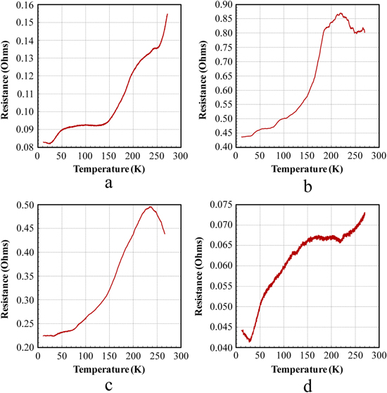
Figure 3. Measured R versus T of four thin films exfoliated from phosphorus-implanted (Ep = 10 keV, dose 1.2 × 108 cm−2) HOPG samples. (a) HOPG-008, layer 3; (b) HOPG-019, layer 3; (c) HOPG-019, layer 6; (d) HOPG-021, layer 7. The layer numbers indicate the number of multilayers peeled from the host sample, i.e. layer 7 would be the seventh layer exfoliated from that sample.
Download figure:
Standard image High-resolution imageComparing figures 3(a)–(d) it is clear that there is a step in resistance at a temperature of approximately 50–60 K in all of the samples. When the data are closely examined it is likewise clear that there is a second resistance step at 100–120 K. Again, at temperatures of approximately 150–180 K and at about 200–240 K there are additional steps in the R versus T characteristics of almost all of the samples. This is cause to suspect that the features are due to magnetic vortex lattice melting and subsequent flux-flow losses.
To see if additional lattice damage by neutral ion species could increase pinning, which could only occur if magnetic vortices were present, and reduce losses, a sample that had been previously implanted with phosphorus but had not been exfoliated was sent back for implantation with argon. This implantation was done at reduced energy (5 keV) and the same dose as the phosphorus implantation (1.2 × 108 cm−2) to place the damage in front of the peak in the phosphorus distribution. A change in the R versus T characteristic that was qualitatively commensurate with stronger pinning would indicate that the resistance was due to flux-flow. Figure 4 shows the computed range distributions for the phosphorus (1) and the argon (3) implants in this HOPG sample and the computed damage distributions caused by implanted phosphorus (2) and argon (4).

Figure 4. This represents the simulated normalized distributions of implanted atoms and lattice damage caused by implanted atoms versus depth in HOPG. Curve 1 is the calculated distribution of the implanted phosphorus, curve 2 is the computed damage caused by the implanted phosphorus, curve 3 is the calculated distribution of the implanted argon and curve 4 is the computed damage caused by the implanted argon.
Download figure:
Standard image High-resolution imageThe R versus T characteristic of an exfoliated graphene multilayer from this doubly implanted sample (phosphorus followed by argon) is shown in curve 1 of figure 5. Note that the first R versus T characteristic taken showed the same qualitative behaviour as the samples in figure 3.
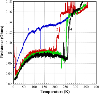
Figure 5. R versus T of a thin film sample peeled off phosphorus-implanted and then argon-implanted bulk HOPG-023. Curves 1 to 4 are four identical sequential runs with the same probe position.
Download figure:
Standard image High-resolution imageA small notch in curve 1 (figure 5) is somewhat too wide (18 data points each from 250 averaged measurements) to be either noise or a measurement glitch. This notch is at a temperature of 132 K and caused us to re-measure the sample multiple times. The re-measurements were performed without moving the contacts or opening the refrigeration system. In these subsequent R versus T re-measurements, shown as curves 2 through 4 in figure 5, a large and abrupt step was observed. The step was in the temperature region of 210–230 K on the first re-measurement. On a second re-measurement it had moved upward to a temperature of 250–260 K. On a third, and final, re-measurement, the step had migrated upwards to a temperature of 264–267 K.
When all four R versus T characteristics for the graphene multilayer from sample HOPG-023 are plotted together on the same graph (figure 5) it is clear that these steps are not a contact issue, as the low temperature and high temperature resistances have not changed significantly from run to run. It is also clear that the notch observed in the first R versus T characteristic is an attempt by the material to move to the resistance state achieved in the later runs and cannot be dismissed as spurious.
The SQUID magnetometer measurements of a doped-while-grown exfoliated thin film are shown in figure 6. They consist of a zero-field-cooled magnetization run followed by a field-cooled magnetization run. The hysteresis loop in the zero-field-cooled to field-cooled curves begins to open at a temperature of approximately 260 K.
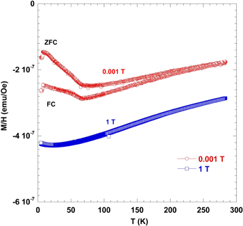
Figure 6. Magnetization measurements: zero-field-cooled (ZFC) and field-cooled (FC) M/H plots along with a 1 T field-cooled M/H plot for a film exfoliated from a doped-while-grown plasma CVD sample.
Download figure:
Standard image High-resolution imageIn addition, when the horizontal axis of the zero-field-cooled magnetization run is converted from temperature to the magnetic field divided by the upper critical field of the vortex state (i.e. from T to H/HC2) and the data are re-plotted, the results are qualitatively consistent with those of Berdiyorov's experiments and calculations [33] as well as the work done by Novosolev [34]. Figure 7 (figure 3.2 in Berdiyorov's work [33]) shows the qualitative shape of a pancake vortex array in a type I superconductor where the thickness is much less than the magnetic penetration depth. Figure 7(d) would be the most relevant to our samples as it has no 'hard pinning' sites (anti-dots).

Figure 7. The free energy (a)–(c) and magnetization (d)–(f) as a function of the applied magnetic field for a filled square (a), (d) and for the square with two (b), (e) and four (c), (f) anti-dots. The insets show the free energy for higher vorticity. The vertical lines show the ground state transitions between different vortex states, and open circles indicate continuous transitions between different vortex states. The GL parameter is k = 0.28 [33].
Download figure:
Standard image High-resolution imageFor comparison to the curves in figure 7(d) the phosphorus-doped-while-grown CVD exfoliated graphene film zero-field-cooled curve of figure 6 has been re-plotted. This re-plotting consisted of converting the temperature information to the ratio of H to HC2 used in figure 7(d) [33]. Since there is no known value for HC2 for the phosphorus-doped-while-grown CVD exfoliated graphene film, the best comparison that can be made is qualitative, in terms of the shapes of the curves. This is shown in figure 8. Note the step in the curve at low H/HC2 in figure 8. This corresponds qualitatively to one of the discontinuous jumps in Berdiyorov's data and, had the measurement temperature been taken to lower values, would most likely have continued vertically.
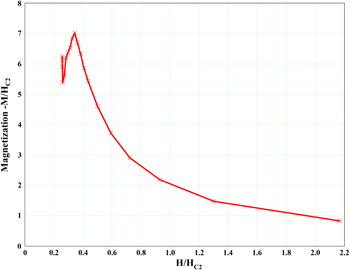
Figure 8. Phosphorus-doped during growth in plasma CVD graphene sample zero-field-cooled magnetization results plotted on the same axis types as used in Berdiyorov's work. Note the same general shape as in figure 7(d).
Download figure:
Standard image High-resolution imageThe ac susceptometer measurements for a representative doped-while-grown exfoliated thin film are shown in figure 9. In addition to each of the full-scale plots, a corresponding plot with a magnified vertical axis is shown. In addition, a representative plot from a known superconductor is included as figure 10. Note that there is a small transition that is broad and begins in the area of 150 K (this may be depressed as a result of the measurement field).

Figure 9. Ac Susceptometer results for a graphene film on Kapton tape exfoliated from a phosphorus-doped-while-grown CVD sample. (a) The film was cut into multiple pieces and the pieces were stacked to increase the screening fraction; (b) magnified vertical axis ac susceptometer results for the same sample and run as shown in (a).
Download figure:
Standard image High-resolution image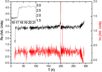
Figure 10. Ac Susceptometer results for a Pr2−xCexCuO4 superconductor in the same instrument as was used to produce the data shown in figure 9. The magnified transition region is shown in the inset.
Download figure:
Standard image High-resolution imageThe final measurements that were done included a Raman spectrum of one of our exfoliated films to estimate the film's thickness (figure 11).
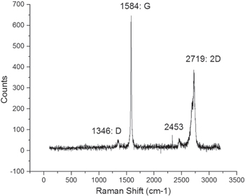
Figure 11. Raman spectra for a film on Kapton tape exfoliated from a phosphorus-doped-while-grown CVD graphene sample. The peak ratios give a thickness of approximately 5 monoatomic layers.
Download figure:
Standard image High-resolution imageHall effect measurements at temperatures of 297 K and 80 K are shown in figure 12. Note that the change of sign in the Hall voltage is real and not due to instrumentation; neither the contacts nor the extraction calculations were altered between the two runs.

Figure 12. Hall effect at T = 293 K and T = 80 K for the same film on Kapton tape exfoliated from a phosphorus doped-while-grown CVD graphene sample, as shown in the Raman spectrum in figure 11.
Download figure:
Standard image High-resolution image
5. Discussion
We have observed a response consistent with the presence of magnetic field flux vortices in phosphorus (electron donor) implanted HOPG and in phosphorus-doped exfoliated multilayer graphene. The repeated nature of the observed steps in the resistance versus temperature characteristics of the material is consistent with the melting of stacks of pancake vortices of differing lengths at different temperatures. The lack of zero resistance at low temperatures is also consistent with pancake vortex behaviour in the flux-flow regime. This allows the use of a single phenomenon, magnetic pancake vortices, to describe the features observed. The presence of magnetic vortices requires, and is direct evidence of, superconductivity. The small Meissner effect may simply mean that the volume fraction of material involved is quite small or that the penetration depth is significantly larger than the sample thickness.
The material that was subjected to post-doping argon implantation (damage) showed a discontinuous step in resistance at a temperature of about 265 K. We noted in our prior work [5], a summary of which is included in the background portion of this paper, that 'the ultimate critical temperature in this system is in excess of 100 K and, may very likely be considerably higher if damage incurred during the doping can be further minimized'. Clearly this conclusion has not been voided and, based on the material with phosphine in the plasma CVD growth gas mixture, may well be valid for a transition at a temperature of greater than 300 K.
6. Conclusions
The repeated steps in the resistance versus temperature characteristics of phosphorus-doped HOPG and graphene are independent of the manner in which the material is doped. Adding damage causes these steps to become nearly discontinuous at elevated temperatures. This is consistent with the results that are expected for thin superconducting films with and without damage.
The lack of zero resistance at low temperature does not fundamentally exclude superconductivity as a mechanism for the material's observed electrical and magnetic behaviour. The high degree of anisotropy in graphite and graphene, in fact, predicts that if the material is a superconductor there would be significant magnetic flux-flow losses even at very low temperatures.
The magnetic response of phosphorus-doped HOPG and graphene is likewise as would be expected for superconductors of similar physical characteristics. That is, (1) the superconducting region is thin in comparison to the London (magnetic) penetration depth and (2) the high level of anisotropy in the material is favourable for the formation of pancake vortices. Additionally it has been demonstrated that the resistance versus temperature curve can be quenched by the application of a magnetic field; this is likewise what would be anticipated from a superconductor.
The magnetization and susceptibility results for phosphorus-doped HOPG and graphene suggest (1) a transition temperature above 260 K for the magnetization based upon the zero-field-cooled to field-cooled hysteresis loop and (2) a transition temperature above 150 K based upon the ac susceptometer measurements. There is no trace of ferromagnetism in the results as both the magnetization and susceptibility are negative in the lower temperature region.
Finally, the Hall effect measurement shows a sign change in the Hall voltage when going from room temperature to 80 K. This is observed in other, known and accepted, superconductors that are in the flux-flow region of the mixed or vortex state. It is also seen in anomalous ferromagnetism. Since there are (1) no ferromagnetic atoms and (2) no atoms with d or f electron shells in the sample, it is highly unlikely that ferromagnetism is involved in these Hall measurements. In addition, the fact that the magnetization and magnetic susceptibility are both negative tends to eliminate ferromagnetism as an explanation for this sign reversal in the Hall voltage.
The aforementioned evidence forces us to conclude that phosphorus-doped HOPG (and phosphorus-doped graphene) is a superconductor with a transition temperature between 150 K and 260 K. In fact, some of our data hints at a possibility that the transition temperature in the best samples may approach room temperature.
This evidence of superconductivity (or another new physical phenomenon) in doped graphene/graphite with a de-pairing (critical) temperature in the region of 260 K is intriguing. Clearly more work needs to be done to confirm the observations and the proposed mechanism of the observed effect. We welcome further investigation into the matter by our colleagues.
Acknowledgments
The authors wish to thank Dr Richard Greene, Dr Paul Bach, Dr Shanta Saha, and Dr Joshua Higgins at the University of Maryland, who tested our samples using SQUID magnetometer and ac susceptometer and whose results are presented in this work. The authors also wish to thank Dr Steven Prawer and Laurens Henry Willems Van Beveren of the University of Melbourne, who performed the Raman and Hall effect characterization of our samples that are presented in this work. The authors would like to recognize Cutting Edge Ions, LLC for ion-implantation doping of our HOPG samples. Finally the authors would like to acknowledge the support of the United States Air Force under AFOSR grant FA9550-10-1-0134 and the guidance of Dr Harold Weinstock of the United States Air Force's Office of Scientific Research.