
Abstract
Recent progress in two-dimensional superconductors with atomic-scale thickness is reviewed mainly from the experimental point of view. The superconducting systems treated here involve a variety of materials and forms: elemental metal ultrathin films and atomic layers on semiconductor surfaces; interfaces and superlattices of heterostructures made of cuprates, perovskite oxides, and rare-earth metal heavy-fermion compounds; interfaces of electric-double-layer transistors; graphene and atomic sheets of transition metal dichalcogenide; iron selenide and organic conductors on oxide and metal surfaces, respectively. Unique phenomena arising from the ultimate two dimensionality of the system and the physics behind them are discussed.
Export citation and abstract BibTeX RIS

Original content from this work may be used under the terms of the Creative Commons Attribution 3.0 licence. Any further distribution of this work must maintain attribution to the author(s) and the title of the work, journal citation and DOI.
List of acronyms
| 1D, 2D, 3D | one-, two-, three-dimensional (dimension(s)) |
| KTB | Kosterlitz–Thouless–Berezinskii |
| BCS | Bardeen–Cooper–Schrieffer |
| S–I | superconductor–insulator |
| MBE | molecular beam epitaxy |
| PLD | pulsed laser deposition |
| UHV | ultrahigh vacuum |
| LT | low temperature |
| STM | scanning tunneling microscopy (microscope) |
| STS | scanning tunneling spectroscopy |
| ML | monolayer |
| FET | field-effect transistors |
| EDL | electric double layer |
| UC | unit cell |
| GL | Ginzburg–Landau |
| AL | Aslamazov–Larkin |
| MT | Maki–Thompson |
| LEED | low-energy electron diffraction |
| QWS | quantum well states |
| SQUID | superconducting quantum interference device |
| ARPES | angle-resolved photoemission spectroscopy |
| FFLO | Fulde–Ferrell–Larkin–Ovchinnikov |
| SOI | spin–orbit interaction |
| FET | field-effect transistor |
| RHEED | reflection high-energy electron diffraction |
| CDW | charge density waves |
| SDW | spin density waves |
1. Introduction
Superconductivity arises from the Cooper pair formation of a huge number of conduction electrons in a metal at sufficiently low temperatures. Since it is a representative order–disorder phase transition, the dimensionality of the system, i.e. one, two, or three dimensions (1D, 2D, 3D), can have a crucial influence on its characteristics [1–3]. Generally, the lower the dimension, the more difficult it is for the phase transition to take place, because the interaction between microscopic constituents of the system (in this case, electrons) becomes spatially limited and a fewer number of partners is available for the interaction with a particular constituent. This means that, even in an ordered phase below the transition temperature (Tc), each subset of the system has a tendency to behave more independently, and the order parameter suffers from larger spatial and temporal fluctuations. In the extreme case, the coherence throughout the system is completely lost and the phase transition itself is destroyed. Now let us ask a simple question: does superconductivity survive in a 2D system, especially when one of the material dimensions is reduced to a truly atomic-scale size? If this is the case, what are the unique characteristics of 2D superconductivity, and what kind of new phenomena are expected to occur? These questions are obviously relevant to modern state-of-the-art nanotechnology and will be crucial issues when the present superconducting devices are shrunk towards the atomic-scale limit in the future [4–6].
There is a long history regarding this problem. First of all, we should note that, for a 2D system, the famous Mermin–Wager theory prohibits the superconducting phase transition that accompanies symmetry breaking and long-range correlation of the order parameter [7, 8]. This does not mean, however, that 2D superconductivity is unrealistic. The Kosterlitz–Thouless–Berezinskii (KTB) transition, which is compatible with the Mermin–Wager theory, can occur in a 2D system and allows the establishment of quasi-long-range correlation of the order parameter [9–11]. In this case, the zero-resistance state is retained for infinitesimally small external perturbation and the Meissner effect can also be well-defined [12, 13]. Even without the KTB transition, Cooper pairs can condense at the mean-field level due to the Bardeen–Cooper–Schrieffer (BCS) mechanism (i.e. Tc0 > TKTB, where Tc0 is the Cooper pair condensation temperature and TKTB is the KTB transition temperature). In a practical sense, the system may be considered superconducting if the correlation of the order parameter is sufficiently developed at low temperatures. Nevertheless, 2D superconductivity is on the verge of transition to a metallic or an insulating state and thus could be fragile. Indeed, introduction of disorder into a 2D superconductor can readily induce a superconductor–insulator (S–I) transition [14], in clear contrast to the 3D counterpart where superconductivity is robust against disorder [15]. Extensive experimental and theoretical efforts have clarified that the S–I transition always occurs when disorder is introduced to such a level that the sheet resistance (2D resistivity) of the sample is of the order of the quantum resistance for Cooper pairs RQ (≡h/4e2 = 6.45 kΩ) [14]. Usually, superconductivity is lost when the thickness of a metal film approaches 1–2 nm and disorder becomes significant [16]. Coming back to the earlier question, the answer should be 'yes' in principle, but realization of a 2D superconductor in the atomic-scale limit has been a technical challenge for a long time. This is because, in this limit, the whole system consists entirely of surfaces and interfaces, which are vulnerable to structural and chemical disorder in general. For this purpose, therefore, it is demanded that samples with highly ordered and controlled surfaces and interfaces should be fabricated and their superconducting properties probed through advanced techniques.
During this decade, the studies on ultrathin 2D superconductors have seen remarkable progress beyond the traditional experimental framework in various fields, and the existence of 2D superconductors with truly atomic-scale thicknesses has also been established. This was mostly driven by rapid advancements in nanotechnology in recent years, including molecular beam epitaxy (MBE), pulsed laser deposition (PLD), in situ ultrahigh vacuum (UHV)-low-temperature (LT) measurement, scanning tunneling microscopy/spectroscopy (STM/STS), etc. These technologies now allow various types of superconducting materials to be fabricated with atomic-scale precision and to be characterized in unprecedented detail, which will be the subject of the present review article. For example, ultrathin elemental metal films grown on silicon surfaces in a layer-by-layer fashion were found to exhibit robust superconductivity down the monolayer (ML) thickness regime [17, 18]. This system also exhibits Tc oscillation as a function of film thickness due to electron quantum confinement effects [19]. La2−xSrxCuO4, a representative cuprate high-Tc superconductor, also showed superconductivity at one unit cell (1 UC) thickness and was electrically tuned to an insulating state, revealing an S–I transition driven by quantum phase fluctuations [20]. Furthermore, the interface between LaAlO3 and SrTiO3, both of them being perovskite oxide insulators, was found to exhibit 2D superconductivity, which can coexist or compete with ferromagnetism [21]. A recent technological breakthrough in field-effect transistors (FET) using an electric-double-layer (EDL) gate has enabled carrier doping with an unprecedentedly high level (n2D ∼ 1014 cm−2) at the subsurface region [22]. This led to the successful realization of field-induced 2D superconductivity in various insulating materials, including SrTiO3 and ZrNCl [23, 24]. Another great invention concerning 2D materials was the exfoliation of atomic sheets from a piece of a layered material, as was first demonstrated for graphene [25]. The search for superconductivity in atomic sheets such as graphene and transition-metal dichalcogenide monolayers is now under rapid progress [26, 27]. One of the most surprising findings in 2D superconductors is the strong enhancement of Tc in 1 UC thick FeSe layers that are epitaxially grown on SrTiO3 substrates; Tc was found to increase remarkably, up to 40–100 K from 8 K of a bulk FeSe crystal by reaching the atomic-scale limit [28, 29]. This phenomenon suggests a possible generic scheme for realizing high-Tc superconductors based on atomic-scale film thinning and a strong interaction with an appropriate substrate. Finally, investigations into 2D superconductors consisting of organic conductors and of rare-earth based heavy-fermion compounds are also under progress, although the number of available publications has been limited so far [30, 31].
The study of 2D superconductors has evolved into one of the most active fields of superconductivity, which is highly relevant for material science, device physics, and instrumental technologies, as well as for fundamental physics. In the present article, the recent progress in 2D superconductors will be reviewed. The main interest here is to overview the topics in various research fields in a comparative way, and to find commonalities and differences among them. This will help us grasp what is unique in 2D superconductors in general, and to understand how new physics and novel phenomena emerge as a consequence of the atomic-scale thicknesses of the materials. It is my great hope that this holistic and comprehensive approach will stimulate research in individual fields, promote interactions among them, and help create a new interdisciplinary realm of research. While the topics treated in this paper share atomic-scale two dimensionality, they are so extensive and diverse in terms of material that it is impossible to cover all the literature in each field. Nevertheless, I believe that even the selected set of work introduced here allows the present goal to be achieved to a considerable degree. The paper is organized as follows. Section 2 briefly reviews 2D superconductors made of granular and amorphous metal thin films, which have been studied since 1970s, mainly from the viewpoint of the KTB and S–I transitions. This will serve as a basis for understanding the progress in more modern 2D materials. Section 3 constitutes the main body of the paper and describes the recent topics of 2D superconductors in individual fields. These 2D superconductors feature high crystallinity and well-defined, sharp interfaces in general. Figure 1 shows a schematic chart where materials dealt with here are roughly categorized in terms of two axes: the horizontal axis reflecting the material and electronic complexity and the vertical axis the location of the 2D superconducting layer, i.e. the top-exposed surface or buried interface. The former may also be labeled with the strength of electron correlations, while the latter with the required experimental technique, i.e. UHV environment or device configuration. Note that the positioning of each field within the chart is only qualitative and subjective. Readers are also referred to table 1 where representative 2D superconductors treated here are listed along with their categories and important attributes. The paper is summarized in section 4.
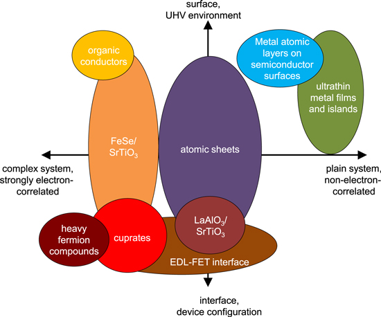
Figure 1. Schematic chart categorizing the materials dealt with in this review. Note that the positioning of each topic is only qualitative and subjective.
Download figure:
Standard image High-resolution imageTable 1.
List of the categories and attributes of representative 2D superconductors with material type, form, thickness (d), superconducting transition temperature (Tc), Tc of the bulk counterpart, Ginzburg–Landau (GL) coherence length at zero temperature (ξGL(0)), and out-of-plane and in-plane upper critical magnetic fields (μ0Hc2⊥(0), μ0Hc2//(0)). Thickness d is defined as the distance between parallel atomic planes that the relevant 2D material would take in bulk form. Regarding Tc,  was determined from the middle point of the resistive phase transition while Tcgap the opening of the superconducting energy gap. In some clear cases, μ0Hc2⊥(0) values were calculated from ξGL(0) using the relation
  by the author (
 magnetic flux quantum). Note that bulk ξGL(0) values are shown for some materials.
| 2D superconductor | Material type | Form | d | Tc | Bulk Tc | ξGL(0) | μ0Hc2⊥(0) | μ0Hc2//(0) | Reference |
|---|---|---|---|---|---|---|---|---|---|
| Pb/Si(111) | Elemental metal | Surface ultrathin film | 2ML (+1ML buffer) (0.57 nm) | 4.9 K 
|
7.2 K | 23 nm (9ML) | 0.62 T (9ML) | — | [78, 17] |
 (rect-phase) (rect-phase) |
Elemental metal | Surface atomic layer | 2ML (0.495 nm) | 3.18 K 
|
3.4 K | 25 nm, 47 nm | 0.49 T | — | [18, 84, 88] |
| Pb/GaAs(110) | Elemental metal | Surface atomic layer | 1ML (0.29 nm) | 0.9 K 
|
7.2 K | 23 nm | 0.6 T | ≫15 T | [101] |
| La2−xSrxCuO4/La2CuO4 | Cuprate | Heteroepitaxial interface | 1 UC (1.3 nm) | 40 K ( max) max) |
40 K | ∼2 nm (ξGL⊥(0), bulk) | — | — | [20] |
| LaAlO3/SrTiO3 | Perovskite oxide | Heteroepitaxial interface | 4 ∼ 11 nm | 0.22 K | 0.3 K (max) | 70 nm | 0.1 T | 2 T | [21, 126, 127] |
| ZrNCl | Nitride compound | FET interface | 0.65 UC (1.8 nm) | 14.8 K ( max) max) |
15.2 K (max) | 12.8 nm | 1.7 T | 50 T | [142] |
| MoS2 | Transition metal dichalcogenide | FET interface | 0.49 UC (0.6 nm) | 10.8 K ( max) max) |
7 K (max) | 8.0 nm | 4 T | 52 T | [146, 147] |
| C6CaC6 | Intercalated graphene | Atomic sheet | 2ML (+1ML Ca) (0.68 nm) | 3 K 
|
11.5 K | 49 nm | 0.14 T | — | [160] |
| NbSe2 | Transition-metal dichalcogenide | Atomic sheet | 1/2 UC (0.63 nm) | 3.1 K 
|
7.2 K | 7.8 nm (bulk) | 2 T | 35 T | [27] |
| FeSe/SrTrO3 | Iron chalcogenide | Surface atomic layer | 1 UC (0.55 nm) | 32 K 109 K 
|
8 K | 4.5 nm (bulk) | >52 T 116 ± 12 T | — | [29, 53] |
| λ-(BETS)2GaCl4 | Organic conductor | Surface molecular layer | 1 UC | 9 ∼ 10 K 
|
4.7 K | 1.6, 12.5 nm (ξGL⊥(0), bulk) | — | — | [30] |
| CeCoIn5/YbCoIn5 | Rare-earth based compound | Heteroepitaxial superlattice | 3 UC (2.27 nm) | 1 K 
|
2.3 K | 7.4 nm | 3.8 T | 9.0 T | [31] |
2. Granular and amorphous 2D superconductors
The Ginzburg–Landau (GL) theory of superconductivity allows the definition of the GL coherence length ξGL, which is the characteristic length scale for spatial variation of the amplitude of the order parameter Ψ. A superconducting film with a thickness d ≪ ξGL is considered to be 2D because Ψ becomes uniform in the out-of-plane direction to avoid a cost in free energy [32]. For conventional (BCS-type) superconductors, ξGL at zero temperature, ξGL(0), is of the order of a few hundred nanometers. Therefore, the thickness of a 2D superconductor may still be much larger than the atomic-scale thickness. It should also be noted that ξGL of an unconventional superconductor with a high Tc can be as small as a few nanometers, which is often of the order of the 1 UC thickness because of large unit cell sizes in these materials.
A straightforward way of preparing a superconducting thin film is the vacuum evaporation of an elemental metal such as Pb and Al on an insulating substrate. This can be followed by deposition of a capping layer (e.g. SiOx) for the purpose of avoiding post-oxidation and contamination. If glass or surface-oxidized silicon is used as a substrate, the metal overlayer often grows in the form of a granular film when the thickness is reduced because of poor wettability of metal on these substrates. This naturally introduces disorder into the metal film, the degree of which can be controlled by the film thickness and is represented typically by the sheet resistance Rsheet [14]. The degree of disorder (and hence Rsheet) can also be controlled by intentional surface oxidation of individual metal granules and by repeating this process several times [33]. Thus a prepared granular superconducting film may be modeled as a Josephson-junction coupled island network in the case of strong disorder, where the junctions are of either tunneling or weak-link type. Within individual metal islands, relatively high crystallinity can be obtained. More uniform thin films can be prepared by quench condensation of an evaporated material on a liquid-He cooled substrate, which strongly suppresses diffusion of adsorbed atoms and/or molecules and formation of large clusters [16]. Sputter deposition of certain alloys can also be used for this purpose. To enhance the uniformity of the film, the substrate is often precoated with a buffer layer. The resulting films have amorphous-like microscopic structures with atomic-scale disorder and defects, and are believed to be spatially homogeneous at larger scales [34]. For the quench-condensed films, electron transport measurements should be performed in situ at the sample preparation cold stage to avoid morphological changes of the film. This experimental setup is advantageous in terms of precise tuning of the film thickness, which in this case is the dominant parameter representing disorder. A disadvantage is that it is difficult to perform a detailed structural analysis of the film. Regarding the superconducting material, elemental metals such as Pb and Bi [34], as well as metal composites and alloys like In2O3 and MoGe, have been used [35, 36]. Note that thin films of amorphous Bi become superconducting at T ∼ 6 K, although bulk crystals of Bi do not.
The effect of the low dimensionality manifests itself as an enhancement of fluctuations, as mentioned earlier. This can be seen first of all as a precursor of the superconducting transition. Namely, a 2D superconductor exhibits a sizable decrease in conductivity, even above Tc, due to the temporal formation of Cooper pairs and the inertia of Cooper pairs after decaying into quasiparticles [37, 38]. Within the microscopic theory of superconductivity, the former is expressed by the Aslamazov–Larkin (AL) term and the latter the Maki–Thompson (MT) term. The contribution of the AL term to 2D conductivity, which is added to the normal conductivity, is given by

where  is a universal constant. The contribution of the MT term is expressed by a similar form that includes material dependent parameters. These effects should appear commonly in all 2D superconductors.
In a 2D system, conduction electrons can be readily localized due to the quantum interference effect in the presence of disorder, which is known as the Anderson localization [39]. Since the resulting insulating state is incompatible with a superconducting state, an S–I transition is expected to take place as the degree of disorder in the system is increased. In this viewpoint, the transition is driven by the suppression of amplitude of the superconducting order parameter Ψ. Alternatively, superconductivity can also be destroyed when the phase of Ψ fluctuates strongly and its coherence is lost. This leads to a quantum phase transition at zero temperature [14, 33, 40]. A number of experiments have been performed in this respect since the late 1970s, a representative result of which is shown in figure 2 [34]. Here, the sheet resistance Rsheet of quench-condensed amorphous Bi films was measured as a function of temperature T while increasing the film thickness. The data clearly show an S–I transition around Rsheet ≅ RQ ≡ h/4e2 (=6.45 kΩ). The presence of this universal constant suggests that the transition is actually a quantum phase transition and can be described by the so-called dirty-boson model, at least near the critical point [41, 42]. In this model, Cooper pairs are treated as composite bosons and the possibility of their breaking into fermionic quasiparticles is neglected. Cooper pairs (bosons) are localized due to the strong disorder in the system, but their very existence is assumed even in the resultant insulating state. In addition to Cooper pairs, superconducting vortices are treated as another kind of competing boson in this model. Because of the duality between the two bosons, i.e. Cooper pairs and vortices, the universal constant of RQ ≡ h/4e2 is deduced for the critical sheet resistance Rc. A number of experiments on disorder-induced S–I transitions in different systems revealed that Rc was close to RQ, but the deviation from this value was often noticed [43]. The failure of the dirty-boson picture may be due to extrinsic effects and/or to oversimplification in the theoretical modeling. Otherwise, it suggests that Cooper pairs are at least partially broken at the critical point as a result of the Anderson localization [44]. How satisfactorily this model applies to a real experiment seems to be dependent on the details of the system.
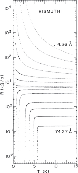
Figure 2. Disorder-induced S–I transition of quench-condensed Bi films. The evolution of the temperature dependence of the sheet resistance R(T) is displayed. The film thickness ranges from 4.36 to 74.27 Å. Reprinted figure with permission from Haviland D B et al 1989 Phys. Rev. Lett. 62 2180 [34]. Copyright 1989 by the American Physical Society. http://dx.doi.org/10.1103/PhysRevLett.62.2180.
Download figure:
Standard image High-resolution imageApart from the particular model, the possibility of a quantum phase transition has also been tested using finite-size scaling analysis [40, 41]. Here the sheet resistance Rsheet of the sample has the following form:

Here, x is a control parameter for the phase transition (e.g., disorder and film thickness) and Rc is the critical resistance that separates the superconducting and the insulating phases, corresponding to x = xc. F(u) is a universal function of u that goes to unity for u → 0. The parameters z and ν characterize the critical behaviors near the quantum phase transition, which gives crucial information on the universality class of the system. The experiment cited above concluded that this scaling analysis worked well, with the extracted parameters of zν = 2.4 and 1.2 for the insulating and superconducting sides of the transition, respectively [45]. The success of this analysis was found in many analogous experiments. In addition to disorder, the magnetic field induces an S–I transition with Rc ∼ RQ, for which the scaling analysis was also successfully applied [35, 36]. All these results evidence the existence of quantum phase transitions in these systems. With technological advancements, the study of the S–I transition has seen new developments. For example, the carrier density of an amorphous Bi layer grown on a thin SrTiO3 substrate was continuously tuned by a gate voltage to investigate this phenomenon quantitatively [46]. High-Tc cuprate superconductors have also become the target of this study. Remarkably, an S–I transition with Rc = RQ and a nearly perfect scaling behavior were demonstrated using a 1 UC thick La2−xSrxCuO4 and an ionic liquid EDL gate (see section 3.5) [20].
Another important phenomenon that is relevant for 2D superconductors in general is the KTB transition [9, 11]. As mentioned earlier, the Mermin-Wagner theory prohibits the emergence of the superconducting phase transition in a 2D system in the strict sense, i.e. the establishment of a long-range correlation at a finite temperature. In a more physical picture, 2D superconductors suffer from phase fluctuations of the order parameter Ψ due to the thermally excited free vortices, even if the amplitude of Ψ is well developed below a Cooper pair condensation temperature, Tc0. When these vortices are moved by an external current in the transverse direction, the motion gives rise to a voltage drop in the longitudinal direction, resulting in finite energy dissipation. This precludes the realization of the true zero-resistance state [32]. However, a vortex in a 2D superconductor can form a bound state with an antivortex (a vortex with the opposite supercurrent circulation) to form a 'neutral' pair. If the vortices interact logarithmically as a function of their separation r like  (
( interaction energy), all vortices and antivortices form pairs below a certain critical temperature, thus leaving no free vortices. This is called the KTB transition, the transition temperature of which is denoted as TKTB. For T > TKTB (and T < Tc0), the average separation ξ between free vortices diverges like
  as T approaches TKTB, and the zero-bias sheet resistance Rsheet decreases to zero according to a relation

Since no free vortices exist for T < TKTB, the true zero-resistance state can be realized. However, the vortex–antivortex pairs become unbound under a finite external current. This unbinding occurs progressively as the current is increased, leading to a current–voltage (I–V) characteristics of a power-law dependence, i.e.  As T is lowered from above TKTB, exponent a jumps universally from 1 to 3 at T = TKTB and increases further at lower temperatures, which is one of the hallmarks of the KTB transition. The phase transition is unique in the sense that it does not lead to a true long-range order, but rather to a quasi-long-range order where the spatial correlation of the order decays as a function of distance according to a power-law dependence. The general features of the KTB transition have been observed using 2D superconductors with moderately high sheet resistances, which were prepared in the similar method as described above [47–49]. Figure 3 shows a representative result of the KTB transition, which was observed for an amorphous homogeneous film made of In/InOx composites with a thickness of 10 nm. Figure 3(a) is a logarithmic plot of the sheet resistance as a function of (T−TKTB)−1/2 where the relation of equation (3) holds over four orders of magnitude in resistance. Figure 3(b) displays I–V characteristics in a log–log plot. The exponent a of the relation
  was found to cross 3 around TKTB = 1.94 K. It should be noted that the occurrence of the KTB transition requires that the logarithmic interaction between vortices be retained up to a sufficiently (ideally, infinitely) long distance. Cutoff of the logarithmic interaction stemming from a finite sample/domain size, a finite perpendicular penetration depth, a residual magnetic field, etc, leads to a non-vanishing zero-bias resistance down to T = 0 [50]. In recent experiments on various 2D superconductors, the KTB transition has been discussed based on non-linear characteristics
  but this relation was found to apply only at relatively high bias regions [21, 51–55]. Whether its origin is ascribed to the interaction cutoff inevitable in real experiments is not clear in many studies.

Figure 3. Experimental identification of the KTB transition. (a) Plot for T > Tc of the logarithm of the resistance as a function of (T−Tc)−1/2 where Tc = 1.903 K. (b) Plot on logarithmic axes of the I–V characteristics taken at thirteen successively lower temperatures ranging from 1.939 K to 1.460 K. Reprinted figure with permission from Hebard A and Fiory A 1983 Phys. Rev. Lett. 50 1603 [48]. Copyright 1983 by the American Physical Society. http://dx.doi.org/10.1103/PhysRevLett.50.1603.
Download figure:
Standard image High-resolution image3. Recent progress in 2D superconductors with atomic-scale thickness
3.1. Ultrathin metal films and islands on semiconductor surfaces
One of the first experiments on superconducting ultrathin metal films with atomically well-defined thicknesses and high crystallinity was performed using Pb films grown on a clean Si(111)-(7 × 7) surface using the MBE method in UHV [56]. An advantage of using these materials is that Pb and Si do not form an alloy so that their interface is atomically sharp. Furthermore, Pb films can grow on a clean Si surface in a layer-by-layer fashion at low temperatures [57], which makes it possible to fabricate ultrathin films with nearly uniform thicknesses. Thus obtained ultrathin Pb films can be an ideal system for studying 2D superconductivity. In [56], the films were characterized using a spot-profile analysis of low-energy electron diffraction (LEED) and the obtained structural information was utilized for the analysis of the transport data. The transport measurements were performed in situ in UHV to exclude contamination and oxidation of the samples. The Tc of the Pb film was found to remain around 5–7 K down to a thickness of 4ML, which was close to the bulk Tc value of 7.2 K. However, the Tc decreased substantially to 1–2 K in the sub-4ML regime, where structural disorder in the macroscopic scale was unavoidable.
A particular interest in ultrathin metal films with atomically smooth interfaces arises from the fact that conduction electrons are quantized in the out-of-plane direction to form quantum well states (QWS). The quantum confinement occurs when the Bohr–Sommerfeld quantization rule is satisfied [58]:

where λ(E) is the electron wavelength at an energy E, d is the film thickness, Φ(E) is the total phase shift at the boundaries, and n is an integer. Since λ(EF) = 1.06 nm for Pb (EF: Fermi energy), d must be both of the order of nanometers and atomically uniform for this effect to be observed. The formation of QWS leads to an oscillation in the electron density of states at the Fermi level, ρ(EF), as a function of d, with the periodicity of λ(EF)/2. Since the Tc of a BCS-type superconductor is proportional to exp[−1/ρ(EF)V] [32], it can lead to an oscillation of Tc as a function of d (here, V denotes the effective interaction between electrons). The first clear observation of this phenomenon was reported using ultrathin Pb films on Si(111) surfaces in the thickness regime above 21ML (see figure 4) [19]. The observed periodicity in d was 2ML, approximately equal to λ(EF)/2 for Pb. The interpretation as a quantum oscillation was supported by the corresponding oscillatory behavior for ρ(EF), which was determined from the temperature dependence of the out-of-plane upper critical magnetic field Hc2⊥ near Tc. In addition, the electron–phonon coupling constant λ appearing in the Eliashberg–McMillan theory [59] was estimated from the temperature dependence of the quasiparticle lifetime through photoemission spectroscopy. This also showed a similar oscillation as a function of d. In this experiment, the transport measurements were performed ex situ with Au capping layers to protect the superconducting Pb layers from air exposure. The presence of the capping layer may shift the energy positions of the quantum well states due to the change in the boundary condition.
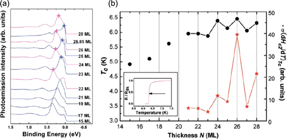
Figure 4. Quantum oscillation of Tc in ultrathin Pb films. (a) Observation of quantum well states in Pb films through in situ photoemission spectroscopy at 75 K. (b) Tc (black solid dots) and the density of states N(EF) ∝ –σ(dHc2/dT)Tc (red stars) as a function of Pb film thickness, demonstrating an oscillatory behavior in both Tc and N(EF). From Guo Y et al 2004 Science 306 1915 [19]. Reprinted with permission from AAAS.
Download figure:
Standard image High-resolution imageAnother important consequence of the QWS in atomically thin Pb films is the manifestation of 'magic thicknesses' during the growth. When the energy positions of QWS are located far from EF for a certain thickness, the film becomes stable due to a decrease in electronic energy. This occurs with a periodicity of λ(EF)/2 and the resulting magic thicknesses are d = 4, 5, 7, 9, ... ML for Pb films [60]. This effect helps to make the film thickness constant at one of these values, and when the nominal coverage of Pb is slightly less than it, flat voids with a lower local magic thickness are created on an otherwise uniform film. The unique morphology leads to a strong pinning of magnetic fluxes at these voids and to the realization of the so-called hard superconductor [32] albeit at atomic-scale thickness. This unexpected robustness of superconductivity was observed for Pb ultrathin films grown on a Si surface by ex situ magnetization measurements using a superconducting quantum interference device (SQUID) [17, 61]. Figures 5(a) and (c) display an STM image of a 7ML thick Pb film with 2ML deep voids and the corresponding d.c. magnetization with a 'hard' hysteresis loop. In contrast, a 7ML thick Pb film with 2ML tall mesas only exhibited a 'soft' hysteresis loop (figures 5(b) and (d)). An analysis of the real and imaginary diamagnetism susceptibility showed that it had a nearly perfect Bean-like critical state corresponding to very hard superconductivity. A critical current density as large as ∼2 × 10⁶ A cm−2 was obtained at 2 K, which was about 10% of the depairing supercurrent density. It was also shown that the structural stability and the superconducting properties could be tuned by adding Bi into Pb to make ultrathin alloy films [62]. Just below Tc, the temperature dependence of Hc2⊥ was found to markedly deviate from the prediction of the GL theory, i.e.  This indicated that, in this 2D geometry, the superconducting order was anomalously suppressed by scattering in violation of Anderson's theorem.

Figure 5. STM images and the corresponding d.c. magnetization loops of ultrathin Pb films. (a), (b) Quantum growth defects in 7ML Pb film consist of either two-atom layer deep voids (a) or two-atom layer tall mesas (b), in films with a small shortage or excess of Pb, respectively. The image size is 700 × 700 nm2 for both (a) and (b). (c), (d) The corresponding d.c. magnetic response of these films. Quantum voids produce 'hard' hysteresis loops (c) , whereas quantum mesas produce 'soft' hysteresis loops (d). Reprinted by permission from Macmillan Publishers Ltd: Özer M M et al 2006 Nat. Phys. 2 173 [17], copyright 2006. http://dx.doi.org/10.1038/nphys244.
Download figure:
Standard image High-resolution imageUltrathin metal films on semiconductor surfaces have been studied not only by the conventional electron transport and magnetic measurements but also by LT-STM/STS. In this case, superconductivity is detected by observing the superconducting energy gap through the measurement of bias-voltage dependent differential conductance (dI/dV). This technique allows direct and real-space investigations of spatially inhomogeneous superconducting properties at atomic scales, which are barely accessible by conventional macroscopic experiments. Since the surfaces of the samples treated here are atomically clean and well-defined, this system is highly suited for STM investigation in UHV. Particularly interesting is the observation of superconducting vortices under application of a magnetic field [63]; the vortex core, where the superconducting energy gap is suppressed due to an excessive supercurrent density, can be imaged as a region with high local density of states (i.e., high dI/dV). Figures 6(a) and (b) show an example of such experiments; 12–14ML thick Pb islands were imaged in (a) the topographic mode and (b) the dI/dV mapping mode with E = EF [64]. In the dI/dV image, the superconducting regions appeared dark due to the presence of an energy gap while the normal-like vortex cores were bright. The vortices were located at the voids, indicating void-induced trapping as discussed above (see also [65]). Furthermore, hysteretic behaviors of vortex dynamics were observed under varying magnetic fields using a Pb island whose size is about several times the coherence length ξGL (~30 nm at 2 K) [66]. The experiment showed that a vortex penetrated into and escaped from the superconducting island at different magnetic fields, revealing the presence of the Bean–Livingston energy barrier at the periphery of the island [67]. In a 2D superconductor with a sufficiently large area, vortices are usually quantized into those with a vorticity of unity and form the Abrikosov lattice, but they can be merged into a giant vortex with a multiple vorticity when squeezed into a narrow region. Such anomalous behaviors were observed for vortices within an ultrathin Pb island using an LT-STM [65, 68].

Figure 6. STM/STS observation of vortices in superconducting Pb islands and the proximity regions. (a) Topographic STM image of Pb islands surrounded by an atomically thin 2D Pb wetting layer. The image size is 1000 × 1000 nm2. (b) Color-coded dI/dV mapping at zero-bias voltage of the same sample area acquired at μ0H⊥ = 60 mT. (c) Characteristic local dI/dV spectra measured at the locations indicated in (a). (d) Zoom of the J1 SNS proximity junction together with corresponding tunneling spectra at three locations at μ0H⊥ = 60 mT. Reprinted by permission from Macmillan Publishers Ltd: Roditchev D, et al 2015 Nat. Phys. 11 332 [64], copyright 2015. http://dx.doi.org/10.1038/nphys3240.
Download figure:
Standard image High-resolution imageWhen a superconductor is in close contact with a normal metal, the superconducting correlations may propagate into the neighboring region [69] where a superconducting energy gap can be detected by a spectroscopic method. This proximity effect is a spatially inhomogeneous phenomenon and has been successfully studied in real space with an LT-STM using superconducting ultrathin Pb islands on a Si(111) surface [64, 70, 71]. Here, 2D atomic layers of Pb (amorphous or crystalline, depending on the sample preparation) on the Si(111) surface played the role of the normal metal region. In a simple configuration, the length scale with which the superconductivity penetrates into the normal metal region is solely determined by the proximity length  where D is the diffusion constant in the normal metal. However, an LT-STM study revealed the presence of a strong geometric effect on the proximity effect [70]. The normal metal region surrounded by superconductors exhibited an enhanced proximity effect, i.e. the energy gap was found to survive up to distances of several times ξM from the boundary. This is due to the quantum interference originating from the multiple Andreev reflection in the confined geometry [72, 73]. At a superconductor–normal metal (S–N) junction, an electron in the N region with an energy −Δ < E < Δ (Δ: energy gap) is reflected as a hole (and vice versa) to allow a Cooper pair injection into the S region, and this Andreev reflection can be multiplied and enhanced in the case of a narrow S–N–S junction. Since the proximity effect is caused by the Andreev reflection, the former is also enhanced by this mechanism. An essentially identical phenomenon was observed when the proximity region was terminated and confined by a surface atomic step [74]. Such an N region in the proximity of an S can host vortices when an out-of-plane magnetic field is applied, which has been successfully imaged using LT-STM [64]. Figures 6(c) and (d) show the superconducting energy gap and its spatial mapping within the proximity N region where a vortex core is visible. The vortex was called a Josephson vortex, since the proximity effect and the multiple Andreev reflection are the origin of the Josephson effect for an S–N–S junction [75]. The locations of these vortices were found to be determined by the spatial distributions of supercurrents within the Pb islands.
3.2. Metal atomic layers on semiconductor surfaces
It has been generally accepted that metal thin films fabricated on a substrate should lose superconductivity when they approach the atomic-scale limit in thickness. In the case of granular and amorphous films, this phenomenon can be understood in terms of the disorder-driven S–I transition as discussed in section 2. However, crystalline thin films with atomically uniform thicknesses for which the disorder is minimized also tend to lose superconductivity in this limit. For example, ex situ magnetic measurements revealed that the Tc of a Pb ultrathin film decreased as a function of thickness d according to the relation:

where Tc0 is the asymptotic value of Tc(d) for d → ∞ (the bulk limit) and dc is the critical thickness for the disappearance of superconductivity [17, 61, 62]. Experimentally, dc was determined to be 0.43–0.615 nm for Pb, which corresponds to 1.5–2ML. Within the framework of the GL theory, this behavior can be naturally explained by the introduction of a surface energy term into the GL free energy [76]. While this term originates from the decrease in density of states near the surface in [76], it could also be attributed to other effects such as surface/interface roughness or disorder, which is hardly avoidable in real experiments (for example, because of a capping layer). Whatever the origin is, superconductivity may persist until the truly monatomic thickness if this effect is negligibly small. In situ UHV-LT-STM experiments on 2D Pb islands on a Si(111) surface showed that this was actually the case [77, 78]. The Tc values, obtained from the analysis of temperature-dependent superconducting energy gap Δ(T), remained between 6.0 K and 6.7 K down to d = 4ML, while Tc = 7.2 K for bulk Pb. Tc was also found to oscillate with a periodicity of 2ML due to the formation of QWS as discussed in section 3.1. Even 2ML thick Pb film, for which only a single QWS channel exists, retained superconductivity with Tc = 3.65 K or 4.9 K depending on the type of Pb–Si interface (i.e. Pb-induced surface reconstructions, see below). It should be noted that a UHV-LT-STM study by another group on the same Pb/Si(111) system found that Tc steadily decreased with decreasing d according to equation (5), where dc was determined to be 1.88 ML [79]. The reason for this discrepancy is not clear, but may be attributed to a subtle difference in the resulting Pb–Si interface structure originating from the experimental conditions.
The naturally grown ultrathin film of Pb on a clean Si(111) surface retains the atomic structure of a bulk crystal while an amorphous-like wetting layer exists at the interface to the silicon substrate, which is the result of the first stage of the Stranski–Krastanov growth mode [80]. This wetting layer can be transformed into a crystalline atomic layer of Pb through an appropriate annealing process. The structural change is driven by formation of covalent bonding between the metal adatoms and the silicon substrate and leads to a unique lattice periodicity and electronic states distinct from those of bulk Pb. The resulting surface structure is called a Pb-induced (generally, metal-induced) silicon surface reconstruction, and is considered an ultimately thin form of the 2D electron system consisting only of the surface and the interface [81]. It might seem that these surface reconstructions are unlikely to become superconducting due to their ultimate 2D character, but recent experiments have changed this view; UHV-LT-STM observations of the energy gap revealed that three kinds of metal-induced silicon surface reconstructions, Si(111)-SIC–Pb, Si(111)-(√7 × √3)–Pb, and Si(111)-(√7 × √3)–In, exhibited superconductivity with Tc = 1.83 K, 1.52 K, 3.18 K, respectively (see figures 7 and 8(a), (b)) [18]. (Here, SIC stands for 'striped incommensurate' and √7 × √3 for the periodicity against the ideally terminated Si(111) surface.) Compared to Tc = 7.2 K of bulk Pb, those of the two Pb-induced surface reconstructions (Si(111)-SIC–Pb, Si(111)-(√7 × √3)–Pb) are much lower, while that of the In-induced surface (Si(111)-(√7 × √3)–In) is comparable to Tc = 3.4 K of bulk In. For the Si(111)-SIC–Pb surface, the vortices were also observed using STM under an out-of-plane magnetic field. The estimated upper critical field is μ0Hc2⊥ = 1.45 T, giving the coherence length of ξGL(0) = 49 nm. Angle-resolved photoemission spectroscopy (ARPES) measurements on these surface atomic layers revealed highly dispersed metallic band structures, which can be understood based on 2D free-electron-like states [18, 82]. Furthermore, the temperature dependence of the electronic band width showed that the electron–phonon coupling constant λ was ~1 for both Si(111)-SIC–Pb and Si(111)-(√7 × √3)–In, being enhanced from the bulk values. This indicates that the Pb–Si and In–Si interfaces play an important role for the occurrence of the BCS-type superconductivity in this atomically thin limit.
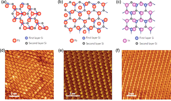
Figure 7. Atomic structural models (a)–(c) and STM images (d)–(f) of metal-induced silicon surface reconstructions: Si(111)-SIC–Pb (a) (d), Si(111)-(√7 × √3)–Pb (b), (e), and Si(111)-(√7 × √3)–In (c), (f). Note that the Si(111)-(√7 × √3)–In surface consists of 2ML of indium according to a recent atomic structure model (Park J and Kang M 2012 Phys. Rev. Lett. 109 166102). Reprinted by permission from Macmillan Publishers Ltd: Zhang T et al 2010 Nat. Phys. 6 104 [18], copyright 2010. http://dx.doi.org/doi:10.1038/nphys1499.
Download figure:
Standard image High-resolution imageThe above finding was based on the tunneling spectroscopy experiments using STM, but more direct evidence of superconductivity was obtained through in situ electron transport measurements under the UHV environment (see figures 8(c), (d)) [83, 84]. The experiments revealed that the emergence of zero resistance, i.e. the existence of supercurrents through atomic layers, and of the superconducting coherence at macroscopic scales. The observed Tc was 1.1 K for Si(111)-SIC–Pb and 2.4 K or 2.8 K for Si(111)-(√7 × √3)–In. The two different values of Tc for Si(111)-(√7 × √3)–In were attributed to the presence of two types of phases that have different nominal coverages of In for this surface reconstruction [85]. It should be noted that the resistance changes were remarkably sharp just at Tc although the systems were in the atomic-scale limit. The decrease in resistance above Tc was accelerated as the temperature approached Tc, which was well described by the 2D fluctuation theories (see section 2) [84, 86]. Analysis of the magnetic field dependence of Tc gave ξGL(0) = 74 nm for Si(111)-SIC–Pb and ξGL(0) = 19–29 nm for Si(111)-(√7 × √3)–In [84]. Unexpectedly, the robustness of the superconductivity at this 2D limit was evidenced in terms of a high 2D critical supercurrent density J2D. For Si(111)-(√7 × √3)–In, I–V characteristics measurements gave J2D = 1.8 × 10⁻² A cm−1 at 1.8 K (correspondingly, a 3D supercurrent density of 3–6 × 10⁵ A cm−2) [83]. The temperature dependence of J2D was described by the Ambegaokar–Baratoff relation [87], suggesting that J2D was determined by Josephson junctions that must exist within the current path on the surface. The most likely locations for the junctions are atomic steps since they terminate and separate the surface terraces. This assignment was corroborated by STM observation of Josephson vortices, which in this case were trapped at the atomic steps on the Si(111)-(√7 × √3)–In surface [88]. The Josephson vortices here are anomalously elongated along the steps and superconductivity is significantly recovered within their core regions. These features are distinct from those of Josephson vortices found in the normal region in the proximity of superconducting Pb islands [64]. The presence of Josephson junctions was also indicated for Si(111)-(√7 × √3)–Pb from the observation of suppressed superconductivity near atomic steps [89].

Figure 8. Superconductivity of Si(111)-(√7 × √3)–In. (a) dI/dV spectra measured on the (√7 × √3)-In phase as a function of temperature using a superconducting Nb tip. (b) Superconducting energy gap Δ as a function of temperature (open circles) and the fitting by the BCS gap function (solid curve). (c) Temperature dependence of zero-bias resistances measured through electron transport measurement. (d) Temperature dependences of critical current Ic (green squares) and retrapping current Ir (pink squares). The blue solid and red dotted lines show theoretical fits. (a), (b) Reprinted by permission from Macmillan Publishers Ltd: Zhang T et al 2010 Nat. Phys. 6 104 [18], copyright 2010. http://dx.doi.org/doi:10.1038/nphys1499. (c), (d) Reprinted figure from Uchihashi T et al 2011 Phys. Rev. Lett. 107 207001 [83]. Copyright 2011 by the American Physical Society. http://dx.doi.org/10.1103/PhysRevLett.107.207001.
Download figure:
Standard image High-resolution imageThere are two unique features that should be considered for atomically thin 2D superconductors in general. First, when a magnetic field is applied in the in-plane direction there exists no orbital pair-breaking effect that usually dominates the upper critical magnetic field Hc2. This is because electrons cannot move in the out-of-plane direction (see figure 9(a)). In the simplest case, the in-plane critical magnetic field Hc2// is determined by the Pauli pair-breaking effect, leading to  at T = 0 where Δ(0) is the BCS energy gap and HP is called the Pauli paramagnetic limit [32]. The low dimensionality of the system and the dominance of the Pauli effect may also lead to a realization of the Fulde–Ferrell-Larkin–Ovchinnikov (FFLO) state at a high magnetic field around HP [90, 91]. This unusual superconducting state is the result of competition between an energy gain due to a partial Cooper pair formation and a paramagnetic energy gain due to the remaining normal electrons, both occurring on the Zeeman-split Fermi surfaces. The Cooper pairs have (multiple) non-zero momentum in striking contrast to the BCS state. Consequently, the order parameter
  becomes spatially modulated with wave vectors of
  even at equilibrium, and is generally expressed by [92]

The second important feature is the manifestation of the Rashba effect due to the space-inversion symmetry breaking of the system and the spin–orbit interaction (SOI) [93]. The Hamiltonian of the Rashba effect is expressed as

where  is the kinetic momentum,
  is the strength of the Rashba SOI,
  is the unit vector perpendicular to the 2D xy plane, and
  is the Pauli matrix. The Rashba effect leads to spin splitting and spin-momentum locking where electron spins are chirally polarized in the directions perpendicular to both the electron momentum and the electric field (see figure 9(b)). Due to the space-inversion symmetry breaking at surface, this effect has been observed by ARPES for metal-induced surface reconstructions with a strong SOI [94, 95]. In terms of superconductivity, the Rashba effect may lead to exotic phenomena under high in-plane magnetic fields. As schematically depicted in figure 9(c), the two Rashba-split Fermi surfaces move in the opposite directions by ±q/2, perpendicular to the magnetic field H// (note that this is a simplified picture and the Fermi surfaces are actually deformed under a high field). This is due to a magnetoelectric effect based on the reconfiguration of momentum-locked spins under a magnetic field [96]. Then the electrons on each Fermi surface can form Cooper pairs with non-zero momentum ±q, leading to
  similarly to equation (6) [97] (see figure 9(d); here the x direction is set parallel to H//). The resulting superconducting state is often called a FFLO-like state, while the original FFLO state is caused purely by the Zeeman effect and does not require the Rashba effect. Another possible consequence of the magnetoelectric effect is induction of unidirectional supercurrents perpendicular to the magnetic field (note that magnetic field usually induces circular supercurrents as a vortex; see also figure 9(d)). Since such stationary supercurrents cannot run in an isolated object, Ψ becomes spatially modulated as
  to compensate the internal supercurrent (note that q' is different from q in the above equation). This state is called the helical state [98]. The FFLO-like state and the helical state compete with each other [99], but the helical state is more robust against the impurity scattering. These exotic superconducting states have unusually high values of Hc2//, and have been studied within the context of heavy-fermion systems (see section 3.8) [92, 100]. Since metal atomic layers on semiconductor surfaces (metal-induced surface reconstructions) treated here are much simpler systems, they may provide a new platform where complexities such as strong electron-correlation effects can be avoided.
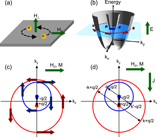
Figure 9. Schematic illustrations of electrons and superconductivity in a 2D system. (a) Effects of the out-of-plane (H⊥) and in-plane (H//) magnetic fields on the electron orbital motion of a Cooper pair. (b) Spin splitting and spin-momentum locking due to the Rashba effect. (c) Shifts of the Rashba-split Fermi surfaces caused by application of H//. The arrows on the circles indicate the directions and the sizes of spin magnetizations. (d) Cooper pair formation on each Fermi circle depicted in (c) and the unidirectionally induced supercurrent J.
Download figure:
Standard image High-resolution imageExperimentally, there have already been reports on surface 2D superconductivity related to these topics. Notably, the Si(111)-(√3 × √3)–(Tl, Pb) surface reconstruction consisting of 1ML of Tl and 1/3ML of Pb on Si(111) was found to exhibit the Rashba effect based on ARPES measurements (see figure 10(a)) [52]. The same surface also showed a superconducting transition at 2.25 K, opening a route for investigating the exotic superconducting state as stated above. In [89], the STS observation of the superconducting Si(111)-(√7 × √3)–Pb surface and the analysis of its energy gap structure indicated the presence of a large pair-breaking parameter. This was attributed to the scattering of the triplet part of the spin-triplet mixed Cooper pairs, which can be caused by the space-inversion symmetry breaking and the resultant Rashba effect [96]. Furthermore, in situ transport experiments on Pb monatomic layers grown on a vacuum-cleaved GaAs surface showed a surprising robustness against an in-plane magnetic field (see figure 10(b) [101]. The Tc was found to decease only by ~2% under an in-plane field of 15 T. This phenomenon was interpreted as a manifestation of the helical state described above, based on the analysis of elastic and spin–orbit scattering rates deduced from the transport data.
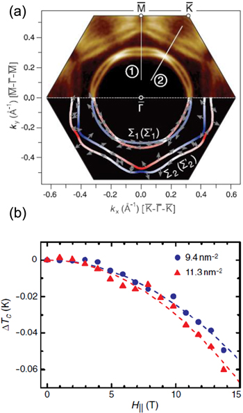
Figure 10. Rashba effects detected for atomic-layer superconductors on semiconductor surfaces. (a) Experimental (upper panel) and calculated (lower panel) Fermi contours of the 2D Tl–Pb compound on Si(111) shown in the √3 × √3 surface Brillouin zone. (b) H∥ dependence of ΔTc (≡Tc−Tc0) for Pb films on a GaAs substrate with n = 9.4 and 11.3 nm−2. The dashed lines are the best parabolic fits. (a) Reprinted figure with permission from Matetskiy A V et al 2015 Phys. Rev. Lett. 115 147003 [52]. Copyright 2015 by the American Physical Society. http://dx.doi.org/10.1103/PhysRevLett.115.147003. (b) Reprinted figure with permission from Sekihara T et al 2013 Phys. Rev. Lett. 111 057005 [101]. Copyright 2013 by the American Physical Society. http://dx.doi.org/10.1103/PhysRevLett.111.057005.
Download figure:
Standard image High-resolution imageFinally, 2ML thick Ga atomic layer on GaN(0001) was found to exhibit superconductivity. The measured sheet resistance showed the onset of a transition at  and appearance of the zero resistance at
  which were much higher than Tc = 1.08 K for the bulk stable phase of α-Ga [102]. This Tc enhancement was attributed to a possible strong interaction at the interface between the Ga layer and the GaN substrate. It is reminiscent of the high-Tc superconductivity of 1 UC thick FeSe layers on a SrTiO3 substrate, which will be described in section 3.7.
3.3. Cuprate: La2−xSrxCuO4/La2CuO4 interface
It is widely recognized that high-Tc cuprate superconductors such as La2−xSrxCuO4, YBa2Cu3O7, and Bi2Sr2CaCu2O8+x have layered perovskite structures where hole-doped conducting CuO2 planes are separated from each other by insulating layers [103]. The bulk crystal retains strong 2D characters because the conduction channels of the CuO2 planes are only weakly coupled (often regarded as Josephson coupled), and the coherence length in the out-of-plane direction (along the c-axis) ξGL⊥(0) is comparable to the UC length. This naturally leads to the following questions: what is the minimum number of CuO2 planes (or unit cells along the c-axis) for the occurrence of superconductivity, and how does the coupling between the CuO2 planes helps establish high Tc in these systems? Indeed, soon after the finding of cuprate superconductors, the investigation into this problem started [104–108]. Generally, superconductivity was found to survive even when the number of UCs in a cuprate thin film was reduced to one. Nevertheless, the temperatures where the zero resistance sets in  were substantially suppressed compared to both the bulk Tc values and the temperatures where the resistance starts to decrease
  For example, a 1 UC thick YBa2Cu3O7 layer sandwiched between 6 UC thick PrBa2Cu3O7 layers showed
  and
and  while Tc ≅ 90 K was obtained for a 100 nm thick YBa2Cu3O7 film [107]. Consequently, the superconducting transition was found to be substantially broadened. It was difficult to determine in the early stages of research whether this is the intrinsic effect due to the ultimate 2D character or it is caused by extrinsic factors such as structural and/or stoichiometric disorder at the interface.
Recent remarkable advancements of MBE/PLD growth and surface characterization techniques have now allowed researchers to investigate cuprate superconductors with ultimately thin layers of CuO2 with unprecedented precision [109, 110]. For example, La2−xSrxCuO4/La2CuO4 heterostructures with atomically sharp interfaces were studied through electron transport and magnetic susceptibility measurements [109]. Here neither La2−xSrxCuO4 nor La2CuO4 layers are superconducting when isolated, since La2−xSrxCuO4 (x = 0.45) is in the overdoped region of metal and La2CuO4 is a Mott insulator. The resulting heterostructure, however, showed superconductivity with Tc ≅ 30 K, which should be attributed to the presence of the La2−xSrxCuO4/La2CuO4 interface. When the top La2CuO4 insulating layer was transformed into a La2CuO4+δ superconducting layer through annealing in ozone atmosphere, Tc reached ≅ 50 K. This value was 25% higher than Tc of a La2CuO4+δ single phase. Furthermore, the transitions were sufficiently sharp so that  was nearly equal to
  The observed sharp transition strongly suggested the completeness of the interface at the atomic scale. The temperature dependence of critical current density Jc obtained from analysis of diamagnetic response showed that the enhanced superconducting region was spatially limited within 1–2 UC thickness around the interface. A subsequent resonant soft x-ray scanning measurement on the La2−xSrxCuO4/La2CuO4 heterostructure (x = 0.36, Tc = 38 K) also revealed that the conducting hole channel was located at the interface over a characteristic distance of ~0.6 nm [111]. This is half the UC length of La2CuO4 (=1.3 nm) where only a single CuO2 plane is included. The existence of the superconductivity within a nominally single CuO2 plane was further demonstrated using δ-doped heterostructures (see figure 11) [110]. Here one of the CuO2 planes of La2−xSrxCuO4/La2CuO4 (x = 0.45) was selectively doped with Zn to suppress superconductivity, identifying the location where superconductivity occurred. Transport and diamagnetic induction measurements revealed that only the second CuO2 plane from the interface located on the La2CuO4 side was responsible for the phenomenon. The conducting holes were found to arise from charge transfer over the interface due to a chemical potential difference, but its exact location was also influenced by the Sr spatial profile.
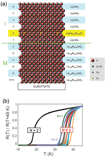
Figure 11. Superconductivity of the La2−xSrxCuO4/La2CuO4 interface. (a) Schematic illustration of 6 UC thick La2−xSrxCuO4/La2CuO4 with δ-doping of Zn atoms at the N = 2 CuO2 plane. (b) Effect of δ-doping with Zn on superconductivity in La2−xSrxCuO4/La2CuO4 bilayer films grown by MBE. From Logvenov G et al 2009 Science 326 699 [110]. Reprinted with permission from AAAS.
Download figure:
Standard image High-resolution imageThe same group also demonstrated that superconductivity of 1 UC thick La2−xSrxCuO4 (x = 0.06 to 0.2) can be electrically modulated [20]. The samples were fabricated through epitaxial growth on insulating La2CuO4/LaSrAlO4 substrates, and the EDL gating technique based on polymer electrolyte or ionic liquid was applied (see section 3.5) to successfully tune the Tc by up to 30 K. This has become possible due to the fact that the thickness of the conduction layer was only ~1 nm and that a huge local electric field of >109 V m−1 was obtained in this configuration. Using underdoped samples in the same setup, they also investigated the S–I transition by modulating the carrier density to reveal its nature as a quantum phase transition (see figure 12). Accumulated data on the sample sheet resistance Rsheet as a function of temperature T and the number of mobile holes per unit cell, x, were found to follow perfectly the scaling equation function given in equation (2) (see section 2). The analysis gave Rc = 6.45 ± 0.10 kΩ and zν = 1.5 ± 0.1. Remarkably, the critical resistance Rc obtained here is equal to the quantum resistance for Cooper pairs, RQ = 6.45 kΩ, within an experimental error. This strongly suggests that Cooper pairs exist in the form of localized bosons in the insulating region near the boundary and that the transition is driven by quantum phase fluctuations [42]. The value of zν = 1.5 is clearly different from those of previously investigated systems, such as amorphous MoGe films (zν ≅ 1.3) [35], a LaAlO3/SrTiO3 interface (zν ≅ 2/3) (see section 3.4) [112], and amorphous Bi films (zν ≅ 0.7) [46]. This means that they belong to different universality classes and that the observed quantum phase transitions are governed by different physics (for example, zν = 4/3 and 2/3 correspond to the classical percolation and the 3D XY models, respectively). Also, related experiments on hole-doped YBaCuO7-x in a similar configuration revealed Rc = 6.0 kΩ and zν = 2.2 [113]. Here, the result Rc ≅ RQ = 6.45 kΩ was also indicative of a phase transition by quantum phase fluctuation of Cooper pairs, but the failure of the scaling analysis at the lowest temperatures suggested a possible presence of an intermediate phase near the transition. For electron-doped Pr2-xCexCuO4 (x = 0.04, 0.1), Rc = 2.88 kΩ and zν = 2.4 were found [114]. The large deviation of Rc from RQ indicated that fermionic quasiparticle excitations, arising from the suppression of Cooper pair formation, played an import role in the transition. These results give an important clue for understanding the physics of high-Tc cuprates. It should also be noted that the superfluid density ns(0) of 2 UC thick Y1−xCaxBa2Cu3O7-δ was determined from the a.c. conductivity measured with the two-coil mutual inductance method [115]. The Tc was found to be proportional to ns(0) near the S–I transition, which was attributed to the quantum fluctuation near a 2D critical point.

Figure 12. Electric-field-induced S–I transition of 1 UC thick La2−xSrxCuO4. (a) Temperature dependence of normalized resistance r = R□(x, T)/RQ of 1 UC thick La2−xSrxCuO4 which is an initially heavily underdoped and insulating film. (b) Scaling of the data with respect to a single variable, with zν = 1.5. The discrete groups of points of collapse accurately onto a two-valued function. Reprinted by permission from Macmillan Publishers Ltd: Bollinger A T et al 2011 Nature 472 458 [20], copyright 2011. http://dx.doi.org/doi:10.1038/nature09998.
Download figure:
Standard image High-resolution imagePreparation of cuprate thin layers with an atomic-scale precision based on MBE or PLD methods as shown above requires highly advanced instrumentation. However, recent progress in mechanical exfoliation of atomic sheets, which was first demonstrated for graphene [25, 116], has now allowed preparation of atomic sheets of Bi2Sr2CaCu2O8+x in a simple and cost-effective way [117]. The prepared atomic sheets with thicknesses down to half UC (including two CuO2 planes) were protected by graphene sheets from degradation and transport measurements were performed. While the sheet resistance Rsheet of the sample increased from a few Ω to 5 kΩ as the sheet thickness was reduced from 270 to 0.5 UC, sharp superconducting transitions were consistently observed, with nearly constant Tc of ~82 K. This indicates that the interlayer coupling does not play an important role for the superconductivity of Bi2Sr2CaCu2O8+x. Superconductivity of exfoliated atomic sheets of other layered materials will be described in section 3.6.
3.4. LaAlO3/SrTiO3 interface
As seen in section 3.3, recent technological advancements have allowed researchers to grow complex oxides in a layer-by-layer fashion and to fabricate oxide heterostructures with atomically sharp and well-defined interfaces. Since many oxide materials have unique properties originating from strong electron correlations and orbital/spin degrees of freedom, the interfaces of oxide heterostructures have a huge potential for realizing exotic and functional artificial 2D materials [118]. One of the most famous examples is the interface between two perovskite transition-metal oxides, LaAlO3 and SrTiO3, where LaAlO3 layers are epitaxially grown on a TiO2-teminated (100) surface of SrTiO3 due to a small lattice mismatch [119, 120]. Although LaAlO3 and SrTiO3 are both wide-bandgap insulators, their interface is known to possess a 2D metallic conduction channel with a high carrier mobility. This has been widely ascribed to a mechanism called 'polar catastrophe', which arises from the discontinuity of ionic characters of oxide layers [121]. While the layers consisting of SrTiO3 are formally charge-neutral [(SrO)0–(TiO2)0], those of LaAlO3 are ionic [(LaO)+–(AlO2)−] (see figure 13(a)). Within the LaO–AlO2 stacking layers, an electrostatic voltage is accumulated and becomes linearly divergent as the number of layers increases, which is apparently unrealistic. This difficulty can be solved by the polar catastrophe where half of the charge of the top-surface LaO layer is transferred to the TiO2 layer of the interface. Consequently, in the simplest case, the TiO2 sheets of the LaAlO3–SrTiO3 interface are doped by 1/2 electron per 2D unit cell to have a carrier density of n2D = 3.4 × 1014 cm−2. The actual interface is much more complex, due to effects such as structural and electronic reconstructions, extrinsic electron doping from oxygen defects, and stoichiometric inhomogeneity. Nevertheless, it generally has a high carrier density (~1013 cm−2) and a low sheet resistance (~103 Ω) even when extrinsic electron doping from oxygen defects is minimized by choosing the appropriate growth condition. [119]. The interface also has a high carrier mobility (~104 cmV−1s−1), indicating the electron scattering due to impurities and defects is weak. Generally speaking, LaAlO3 growth at a lower oxygen pressure leads to a higher density of oxygen-deficiency defects in the SrTiO3 substrate and the electron conduction becomes more bulk-like due to the doping [122].

Figure 13. Superconductivity of the LaAlO3/SrTiO3 interface. (a) Schematic illustration of the LaAlO3/SrTiO3 interface. (b) Scanning transmission electron microscopy (STEM) image of a LaAlO3/SrTiO3heterostructure. A 15 UC thick LaAlO3 film was grown on SrTiO3 showing a coherent interface. (c) Dependence of the sheet resistance on T of the 8 UC and 15 UC samples. (d) Temperature dependence of the out-of-plane upper critical field Hc2⊥ of the two samples. (e) V–I curves on a logarithmic scale at different temperatures. The two long black lines correspond to V = RI and V ∼ I3 dependencies. (a) Reprinted by permission from Macmillan Publishers Ltd: Ohtomo A and Hwang H Y 2004 Nature 427 423 [119], copyright 2004. http://dx.doi.org/10.1038/nature02308. (b)-(e) From Reyren N et al 2007 Science 317 1196 [21]. Reprinted with permission from AAAS.
Download figure:
Standard image High-resolution imageRemarkably, electron transport measurements have revealed that the LaAlO3/SrTiO3 interface becomes superconducting at low temperatures (see figures 13(b)–(e)) [21]. For a representative result using a sample with a 8 UC thick LaAlO3 layer, important physical quantities related to superconductivity were given as follows: transition temperature Tc ≅ 200 mK, 2D critical supercurrent density Jc,2D = 98 μA cm−1, out-of-plane critical magnetic field μ0Hc2⊥ = 65 mT. The observed Tc was within the range of those previously reported for oxygen-defect-doped bulk SrTiO3 [123]. The GL coherence length at zero temperature was estimated to be ξGL(0) ~70 nm from the temperature dependence of Hc2⊥. Other parameters regarding the electron transport were as follows: sheet resistance Rsheet ≅ 300 Ω, Hall carrier density ≅4 × 1013 cm−2, carrier mobility ≅350 cm V−1s−1 (all at T = 4.2 K). The significant contribution of the interface conduction channel to the transport phenomena and the 2D character of superconductivity were discussed from the viewpoint of the KTB transition. TKTB = 188 mK was obtained from the analysis of the temperature dependence of the I–V characteristics, where the exponent a of the relation  was found to cross the universal constant of three. In addition, the zero-bias resistance was found to follow equation (3), giving TKTB = 190 mK, consistent with the above value. It should be noted that the KTB transition considered here is not of the conventional type where vortex–antivortex bound pairs are formed from thermally excited free vortices in a 2D superconductor; rather it is analogous to the dislocation-induced melting of a 2D crystal treated in the original paper by Kosterlitz and Thouless [9]. Just below Tc, a high density of vortices and antivortices can form an ionic-like crystal if the energy required for thermal excitation of a vortex is sufficiently small. In this case, the KTB transition is characterized by the freezing of vortex-lattice defect motion, which leads to the occurrence of true zero resistance in the limit of an infinitely small bias current [124, 125]. In [21], the residual ohmic regime at small currents observed even below TKTB was attributed to the finite sample size effect [50].
The KTB transition observed here indicates that superconductivity in this system is of 2D character, thus limiting the maximum thickness of the conducting layer sufficiently below the coherence length of ξGL(0) ~70 nm. A subsequent experiment on the same system revealed the strong anisotropy of a critical magnetic field (Hc2///Hc2⊥ ≅ 20) and showed that the LaAlO3/SrTiO3 superconductivity had indeed a strong 2D character [126]. The thickness of the conduction layer was estimated to be 11 ± 3 nm from the analysis of temperature dependence of the critical magnetic fields. More direct information on the conducting layer thickness was obtained with a microscopic imaging technique based on atomic force microscopy (AFM) [122]. The local resistance was mapped over the cross-section cut of a LaAlO3/SrTiO3 heterostructure using an AFM tip to investigate the extent of the conducting region near the interface. For samples prepared by annealing around 750 °C at an oxygen pressure of 300 mbar after the LaAlO3 growth, the spatial extension of the conducting layer was found to be smaller than 7 nm. By contrast, it could spread up to as large as ~500 μm when a different annealing process was taken due to oxygen-deficiency doping. Furthermore, hard x-ray photoelectron spectroscopy taken on similarly prepared samples revealed that doped electrons are located at Ti sites of the TiO2 layers within a distance of 4 nm from the interface [127].
Thanks to an extremely high dielectric constant of SrTiO3 (εr ~ 300 at room temperature and ∼20 000 at LT) and a carrier density much lower than those of usual metals, the 2D conduction can be electrically tuned using a back gate on the substrate [120]. Superconductivity in this system was electrically enhanced based on this method where the maximum KTB transition temperature TKTB reached 310 mK [112]. Clear S–I transitions were also demonstrated through electrostatic gate control. The critical sheet resistance for the transition was Rc ≅ 4.5 kΩ, which was close to, but lower than, the quantum resistance of Cooper pairs, RQ = 6.45 kΩ [14]. The transition temperature identified with TKTB was found to scale with the carrier density n2D according to a relation  where n2D,c is the critical carrier density for the S–I transition and
  is a parameter related to the critical behavior near the transition (see equation (2) of section 2). The successful application of the scaling theory and the value of
  indicate that the transition is driven by the quantum fluctuations of Cooper pairs in a clean 2D system. Furthermore, a large negative magnetoresistance observed for the insulating phase in the same experiment was attributed to the weak localization of electrons.
Intriguingly, the LaAlO3/SrTiO3 interface exhibits not only superconductivity but also ferromagnetism, as in a theoretical prediction of ferromagnetic alignment of local spins at Ti3+ sites of the interface TiO layer [128]. Experimentally, the existence of a ferromagnetic phase was first reported using samples prepared in high oxygen pressures (i.e. with small oxygen-deficiency doping) nearly simultaneously as superconductivity was discovered for the same system [129]. A clear magnetic-field hysteresis of sample sheet resistance Rsheet was found as an evidence for the formation of ferromagnetic domains, and a logarithmic temperature dependence of Rsheet and a large negative magnetoresistance observed at low temperatures were attributed to the presence of local magnetic moments. Subsequent studies have revealed that superconductivity and ferromagnetism can coexist within the same sample. Magnetic-field dependence of superconducting transition temperature Tc, which was electrically tuned by a back gate, was found to have hysteresis within the range −30 mT < μ0H < −30 mT [130]. This clearly indicated that two conduction channels, corresponding to superconducting and ferromagnetic regions, existed within the interface. More direct evidence for this unexpected phenomenon was soon reported by two independent groups. A combined experiment based on high-resolution magnetic torque magnetometry and electron transport measurements revealed the presence of magnetic ordering in a superconducting LaAlO3/SrTiO3 interface [131]. Also reported was the real-space 2D mappings of magnetization and diamagnetic susceptibility using a SQUID, demonstrating the existence of nanoscale phase separation of ferromagnetic and superconducting regions (see figure 14) [132]. Ferromagnetic domains were observed as separate dipoles and persisted over the whole temperature range of the experiment, while inhomogeneous superconducting domains appeared below 100 mK. A control experiment using Nb δ-doped samples showed that magnetism in this system could only arise from the interface. It should be noted that the space-inversion symmetry is broken at the interface, which is important for the emergence of the Rashba effect (see section 3.2). The SOI needed for the Rashba effect was also detected and was successfully controlled by a gate voltage [133]. Together with the electric-field tunability and the coexistence with ferromagnetism, the LaAlO3/SrTiO3 system offers a platform for exploring exotic superconducting phenomena.
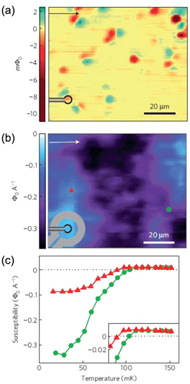
Figure 14. Coexistence of superconductivity and magnetism in the LaAlO3/SrTiO3 interface. (a) Magnetometry image mapping the ferromagnetic order. (b) Susceptometry image mapping the superfluid density at 40 mK. (c) The temperature dependence of the susceptibility taken at the two positions indicated in (b). Reprinted by permission from Macmillan Publishers Ltd: Bert J A et al 2011 Nat. Phys. 7 767 [132], copyright 2011. http://dx.doi.org/10.1038/nphys2079.
Download figure:
Standard image High-resolution image3.5. Electric-field-induced interface superconductivity
In the preceding two sections, we have seen that the interface between two non-superconducting (metallic or insulating) materials may spontaneously host a conduction channel with 2D superconductivity. Realization of such an interface superconductivity in an artificial and controlled way, preferably in a field-effect transistor (FET) configuration, should provide great opportunities for basic physics, materials science, and device applications [134]. In the case of the SrTiO3 substrate, the back-gate control was possible due to its high dielectric constant [112], but the real power of this approach was demonstrated based on an electrochemical method, i.e., using an EDL as a gate electrode (also see section 3.3) [23, 24]. The conventional FET device uses a gate insulator made of a solid-state dielectric material such as SiO2 and high-k complex oxides, but the accumulation of carriers at the interface is limited up to the level of n2D ∼ 1 × 1013 cm−2 because of current leakage and dielectric breakdown of the insulator. In an EDL transistor, however, the solid-state gate insulator is replaced by a liquid electrolyte, which allows free cations or anions to be assembled at the liquid–substrate interface under the application of a gate voltage [22, 135–137]. The resulting EDL works as a subnanometer-gap capacitor and can induce carriers with an areal density up to ∼1 × 1015 cm−2 at the interface (more precisely, at the subsurface) of the target material.
In the early stages of the EDL device, a polymer electrolyte consisting of KClO4 and polyethylene oxide was used to fabricate an n-type FET with a 2D channel at the SrTiO3 interface [23]. This device successfully induced superconductivity at Tc ∼ 0.4 K under the application of the gate voltage above 2.5 V. This is the first report on electric-field-induced superconductivity in an insulator without chemical doping. A substantially high density of electron carriers with n2D = 1 × 10¹³ ∼ 1 × 1014 cm−2 was confirmed through Hall resistance measurements. This corresponds to a 3D carrier density as high as 3 × 1018 cm−3–1 × 1020 cm−3, which is roughly equal to that of superconducting Nb-doped SrTiO3 bulk samples with Tc = 0.4 K. The effective thickness of the conduction channel was estimated to be 5–15 nm based on the calculated spatial distribution of carriers. This relatively large value is due to the large dielectric constant of SrTiO3, which is on the verge of a transition to ferroelectricity. The analysis showed that several 2D quantized subbands were involved within the conduction channel; in this sense, the system is not considered a superconductor in the 2D limit.
Substitution of the polymer electrolyte with ionic liquid, which is an organic salt in the liquid state even at room temperature, enables an even stronger gating function and accumulation of a higher density of carriers at the interface [138]. This has allowed investigation of field-induced superconductivity using various kinds of insulators including ZrNCl, KTaO3, and 1T-TiSe2. Some of the insulators also exhibited many-body quantum states featuring, e.g., magnetic ordering and charge density waves (CDW) [24, 139–141]. The experiment on thin layers of ZrNCl, obtained by mechanical micro-cleavage, realized for the first time superconducting transitions with Tc = 12 ∼ 15.2 K under the gate voltages of 4–5 V using a EDL-FET device (see figure 15) [24]. The measured net carrier density amounted to 1.7 × 1014 cm−2. This seminal work was followed by a more elaborate experiment that revealed many intriguing phenomena (see figure 16) [142]. Generally, quasi-2D bulk superconductors made of weakly coupled conducting layers have an angular dependence on the upper critical magnetic field Hc2(θ), where θ is the angle of magnetic field relative to the in-plane direction (note that, in figure 15(a), θ is measured relative to the out-of-plane direction). Within the 3D anisotropic GL model, the anisotropy can be expressed by the following equation [32]:

This form applies when the coherence length in the out-of-plane direction, ξGL⊥, is larger than the interlayer distance. By contrast, for an isolated 2D superconductor with a thickness much smaller than the magnetic penetration depth, Hc2(θ) obeys the relation:
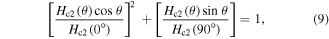
which is called the 2D Tinkham model [143]. The clear difference in the angle dependence between the two model can be found around θ = 0°; for the former, the change in Hc2(θ) is smooth (i.e.  , while for the latter it exhibits a cusp-like shape (i.e.
  In [142], Hc2(θ) for the field-induced superconductivity of ZrNCl exhibited a huge anisotropy between the in-plane (θ = 0°) and out-of-plane (θ = 90°) directions. Furthermore, a cusp-like angle dependence of Hc2(θ) was found around θ = 0°, which was well described by equation (9) of the 2D Tinkham model. From the analysis of the angle dependence, the thickness of the superconducting region was determined to be 1.8 nm. This value corresponds to the (ZrNCl)2 bilayer thickness and is smaller than the 1 UC thickness of ZrNCl (=2.76 nm). Thus it is considered a superconductor in the 2D limit. Correspondingly, the 2D signatures of the KTB transition and the superconducting fluctuation were found from the analysis of temperature dependence of the zero-bias resistance (see section 2). This atomically thin 2D superconductor is relatively clean; the electron mean free path was estimated to be 18–35 nm from the normal sheet resistance, and this value is comparable to Pippard's coherence length ξPippard = 43.4 nm (
 Fermi velocity,
  BCS energy gap at T = 0). This ideal 2D character and high crystallinity led to an almost free vortex motion under magnetic fields of μ0Hc2⊥ > 1.3 T. For 0.05 T < μ0Hc2⊥ < 1.3 T, a quantum creep motion of the vortex lattice was indicated, and the detected finite residual resistances at the lowest temperatures demonstrated the presence of metallic states in this regime [144]. True superconducting states with undetectable residual resistance were obtained only for μ0Hc2⊥ < 0.05 T. The result is contradictory to the theoretical prediction of the dirty-boson model where there should be no metallic state between the superconducting and the insulating states [41]. Accordingly, the magnetic-field dependence of the Rsheet–T relations did not follow the scaling equation of equation (2), thus clarifying the limitation of the conventional theories of the magnetic-field-induced S–I transition when applied to a clean system.
Figure 15. Electric-field-induced superconductivity of ZrNCl. (a) Schematic diagram of charge accumulation by an EDL formed at an interface between ionic liquid and solid. (b) Ball-and-stick model of a ZrNCl single crystal. (c) Channel sheet conductance σs, sheet carrier density n2D and Hall mobility μH of the ZrNCl-EDL transistor modulated by the gate voltage VG from 0 to 4.5 V at 220 K. (d) Temperature dependence of sheet resistance Rs showing superconductivity transitions at different gate voltages, VG. Reprinted by permission from Macmillan Publishers Ltd: Ye J T et al 2010 Nat. Mater. 9 125 [24], copyright 2010. http://dx.doi.org/10.1038/nmat2587.
Download figure:
Standard image High-resolution image
Figure 16. Superconductivity of ZrNCl in the 2D limit. (a) Angular dependence of the upper critical fields μ0Hc2(θ). Note that the definition of the magnetic field angle θ is different from that in the text. (b) Arrhenius plot of the sheet resistance of a ZrNCl-EDL transistor at VG = 6.5 V for different magnetic fields perpendicular to the surface of ZrNCl. (c) Vortex phase diagram of the ZrNCl-EDL transistor. From Saito Y et al 2015 Science 350 409 [142]. Reprinted with permission from AAAS.
Download figure:
Standard image High-resolution image2H-type MoS2, a band insulator and a representative transition metal dichalcogenide, was also turned into a superconductor using an EDL transistor device with ionic liquid [145, 146]. The induced carriers with an areal density of ∼1014 cm−2 were estimated to concentrate within a thickness of ∼0.6 nm, which corresponds to a monolayer of MoS2 (half the unit cell of a MoS2 layered crystal). In addition, a high Hall mobility of ∼240 cm2 V−1 s−1 was obtained at 20 K. Most intriguingly, the superconducting state had a dome-like phase diagram [146] that was reminiscent of those of cuprate high-Tc superconductors [103]. Namely, Tc plotted as a function of 2D carrier density n2D was found to have a maximum value of 10.8 K at n2D = 1.2 × 1014 cm−2. Further increase in n2D resulted in a lower Tc. The Tc = 10.8 K is ∼40% higher than the maximum Tc of alkali-doped bulk MoS2 crystal.
The fact that electron carriers are confined within a MoS2 monolayer has a remarkable consequence, as explained in the following (see figure 17) [54, 147]. MoS2 as a bulk crystal has global inversion symmetry due to its D6h symmetry, and its superconducting state is considered conventional. However, the monolayer of MoS2 lacks in-plane inversion symmetry because it has half the unit cell of a bulk crystal and the symmetry is lowered to D3h [148]. Together with a large SOI originating from the Mo d-orbitals, this causes an effective Zeeman field of the order of ∼100 T and spin polarization in the out-of-plane direction. In the momentum space, carriers induced in the MoSe2 monolayer are located at electron pockets around the K and K' points in the Brillouin zone. The sign of the Zeeman splitting is inverted between the K and K' points due to the time-reversal relation, which is called spin-valley locking [149]. The Hamiltonian for this effect is expressed as

where  is the kinetic momentum in the K and K' valleys,
  is the momentum of the K valley,
  is the valley index,
  is the strength of the intrinsic SOI, and
  is the z-component of the Pauli matrices. When Cooper pairs are formed by two electrons with opposite spins (up and down) and momenta (at K and K'), the only allowed spin directions are along the out-of-plane direction. The resultant state, called Ising superconductivity, is robust against the in-plane magnetic field because the spin polarization direction is perpendicular to the field. Although the spin-valley locking is analogous to the in-plane spin-momentum locking that originates from the Rashba effect (see equation (7) in section 3.2) [52, 101], they are different in terms of the locking direction. Experimentally, huge in-plane critical magnetic fields Hc2// were observed for MoS2 EDL transistors and were attributed to the spin-valley locking phenomena. The observed μ0Hc2// = 52 T at 1.5 K (for Tc = 9.7 K) [147] and μ0Hc2// > 20 T at 1.46 K (for Tc = 2.37 K) [27] are about four to five times larger than the Pauli paramagnetic limit HP. These Hc2// values are also an order of magnitude larger than those of alkali-doped bulk MoS2 crystal, for which Hc2// is dominated by the orbital pair-breaking effect caused by the interlayer coupling. It should be noted that a huge Hc2// value surpassing the Pauli limit was also indicated for the 2D superconductor with the Rashba effect, as discussed in section 3.2, but its origin is different. In the system with in-plane inversion symmetry breaking like the MoS2 monolayer, the presence of the Rashba effect tends to weaken the spin-momentum locking because their spin polarization directions are orthogonal.

Figure 17. Spin-valley locking and Ising superconductivity. (a) Spin-split conduction-band electron pockets near the K and K' points in the hexagonal Brillouin zone of monolayer MoS2. (b) Side view (left) and top view (right) of the four outermost layers in a multilayered MoS2 flake. (c) Temperature dependence of Bc2 (=μ0Hc2) for superconducting states with different Tc. (d) Bc2 normalized by the Pauli limit Bp (=μ0Hp) as a function of reduced temperature T/Tc, including superconducting states from alkali-doped bulk phases and gated-induced phases. From Lu J M et al 2015 Science 350 1353 [54]. Reprinted with permission from AAAS.
Download figure:
Standard image High-resolution image3.6. Atomic sheets: graphene and transition metal dichalcogenide atomic layers
In 2004, graphene was mechanically exfoliated from a piece of graphite to fabricate an high-performance ambipolar FET device for the first time [25]. This invention was followed by the discovery of the half-integer quantum hall effect at low temperatures that signified the presence of massless Dirac fermions [150, 151], and quickly by an explosive number of graphene-related work. Finding superconductivity in graphene has been a long-standing goal in this field and should also greatly contribute to the study on 2D superconductivity. Up to now, however, superconductivity has not been reported in pristine graphene except for graphene-based junctions where Josephson supercurrents were detected to run [152]. This is presumably because of a small density of states at the Fermi level near the Dirac point. Nevertheless, it is well known that graphite intercalation compounds with foreign alkaline or alkaline-earth metal layers exhibit superconductivity, examples of which include KC8 with Tc = 0.14 K [153], CaC6 with Tc = 11.5 K, and YbC6 with Tc = 6.5 K [154, 155]. The metal layers play important roles in terms of the BCS-type superconductivity because they donate electrons into the π*-bands of graphite and modify the electron–phonon interaction. They also form electronic bands by themselves, which affect the total properties of graphite. This raises a hope that intercalated or chemically doped graphene may become superconducting.
Recently, metal-doped few-layer graphene was reported to exhibit superconductivity in a variety of experiments. For example, a wet chemistry method allowed preparation of K-doped few-layer graphene from graphite flakes in dimethoxyethane solution, and superconductivity with Tc = 4.5 K was found based on magnetic susceptibility measurements [156]. Similarly prepared Li-intercalated few-layer graphene was found to have Tc = 7.4 K from magnetization measurements, although transport measurements did not show the evidence of resistance decrease around that temperature [157]. In terms of controlling the quality of graphene and the number of its layers, it is preferable to grow graphene in a layer-by-layer fashion on a semiconducting substrate such as SiC under the UHV environment. Thus prepared multi-layer graphene was Ca-intercalated ex situ by following the standard intercalation method used for bulk compounds [158]. Both magnetic and transport measurements revealed superconducting transitions down to a thickness of 10ML, with the maximum Tc of 7 K. However, since the intercalated dopants of alkaline or alkaline-earth metal are very reactive in air, the above experiments may have been influenced by sample degradation due to air exposure, particularly when the number of layers is very small. To avoid such an undesirable effect, Ca-intercalated bilayer graphene (C6CaC6) was fabricated by growing graphene on a 6H-SiC(0001) substrate and subsequently by depositing Ca in UHV [159]. The samples were characterized by STM and ARPES to reveal their atomic-scale structures and free-electron-like interlayer electronic bands. Furthermore, transport measurements were taken on similarly prepared C6CaC6 samples in situ using a micro four-point-probe technique under magnetic fields, which revealed  and
and  (see figure 18) [160]. Analysis by reflection high-energy electron diffraction (RHEED) showed that intercalated Ca atoms formed a (√3 × √3)-R30° structure against the C(1 × 1) surface of the host graphene and that this structural ordering was crucial to have a clear superconducting transition. However, they did not observe a superconducting transition for Li-intercalated bilayer graphene (C6LiC6). This is puzzling because an ARPES study on Li-intercalated monolayer graphene (LiC6) prepared using a similar method indicated the emergence of superconductivity at Tc ∼ 5.9 K through observation of an energy gap opening at the Fermi level [161]. In this experiment, the occurrence of superconductivity was ascribed to the enhancement of the electron–phonon coupling constant λ to 0.58, which was estimated from the ARPES measurement of the electronic bands. Indeed, first-principle calculations on LiC6 assuming the (√3 × √3)-R30° structure of Li adatoms on a monolayer graphene predicted that Tc would be strongly enhanced to 8.1 K from the bulk value of 0.9 K [162]. This enhancement was attributed to an increase in the electron–phonon coupling constant λ, in line with the experiment. The same theory also predicted Tc = 1.4 K for Ca-intercalated monolayer graphene (CaC6), which is suppressed significantly from the bulk value of 11.5 K. Nevertheless, direct evidence of superconductivity of doped monolayer graphene is so far missing from the viewpoint of electron transport or magnetization measurements. Coming back to the bulk material, superconductivity of intercalated graphene laminates were recently studied [163]. This layered material is similar to bulk graphite, but the coupling between the individual layers is weaker due to the presence of rotational disorder. Thus its electronic structure should be close to that of isolated monolayer graphene. The Tc of Ca-intercalated graphene laminates was found to be ∼6 K at maximum, but it was strongly dependent on the sample condition. K, Cs, nor Li induced superconductivity in the temperature range of T > 1.8 K.
Figure 18. Superconductivity of a Ca-intercalated bilayer graphene. (a) Schematic view of the crystal structure of C6CaC6 on SiC. (b) Band dispersions at the K point of pristine bilayer graphene obtained by ARPES. (c) RHEED pattern showing √3 × √3 R30° spots and streaks. (d) Schematic diagram of the four-point-probe measurement setup. (e) Comparison of temperature dependence of sheet resistance Rsheet between C6LiC6 and C6CaC6. Reprinted from Ichinokura S et al 2016 Acs Nano 10 2761 [160] under an ACS AuthorChoice License. http://dx.doi.org/10.1021/acsnano.5b07848.
Download figure:
Standard image High-resolution imageThe mechanical exfoliation of graphene from graphite has motivated the creation of atomic sheets from layered materials using the same method. In particular, studies on atomic sheets of transition metal dichalcogenides are now very active, in view of valleytronics (electronics combined with the valley degree of freedom in certain semiconductors) and optoelectronics applications [164]. Since the layers of transition metal dichalcogenides are only weakly bonded through van der Waals forces, the technique of mechanical exfoliation is readily applicable. In terms of studies on superconductivity in the 2D limit, NbSe2 is a promising material because it has a relatively high Tc of 7.2 K in the bulk form. It also has a phase transition accompanying CDW at 33 K, so the competition or coexistence of the two ordered states in the 2D limit would also be interesting to investigate. An early experiment in 1972 already reported on the exfoliation of atomic sheets of NbSe2 from a bulk crystal and the electron transport data indicative of the superconducting transition at a few UC thickness [165]. However, recent studies reported the absence of superconductivity in this regime [166], suggesting that the sample degradation due to air exposure and the lithography process was a serious problem. This was solved by performing the whole sample treatment in a controlled inert atmosphere and by encapsulating the target atomic sheet using a graphene or BN atomic sheet [167]. With this technique, monolayer (half UC thick) NbSe2 was found to exhibit superconductivity with Tc ≅ 2 K. Similarly prepared monolayer NbSe2 showed a superconducting transition at 3 K, while a strong enhancement of the CDW transition up to Tc = 145 K was detected from the Raman spectroscopy measurement [168]. High-quality monolayers of NbSe2 were also prepared by MBE growth on epitaxial bilayer graphene on a 6H-SiC(0001) substrate under UHV environment [26]. After addition and removal of a Se capping layer, electron transport measurements were taken to reveal a superconducting transition with  and
and  The suppression of Tc compared to that of bulk NbSe2 was partly attributed to the reduction of density of states at the Fermi level, which was caused by changes in electronic band structures in the monolayer of NbSe2. STM/STS observations also clarified the occurrence of the CDW phase in the same sample. The 3 × 3 CDW superlattice was found to set in around 25 K and to develop fully at 5 K, while there was no signature of the CDW phase at 45 K. This is contradictory to the Tc enhancement observed in [168].
Exactly like MoS2, the NbSe2 monolayer is of half UC thickness and lacks the in-plane inversion symmetry. Together with a strong SOI of transition metal Nb, this can lead to spin-valley locking, as observed for the field-induced superconductivity in the MoSe2 EDL transistors [54, 147] (see section 3.5). This expectation was recently demonstrated by using a mechanically exfoliated NbSe2 monolayer that was encapsulated by thin layers of BN, which exhibited superconductivity with Tc = 3.0 K [27]. Magnetotransport measurements showed that superconductivity was remarkably robust against an in-plane magnetic field, with an estimated upper critical field at zero temperature μ0Hc2//(0) ∼ 35 T. This value is more than six times the Pauli paramagnetic limit μ0HP. Analysis of the temperature dependence of Hc2// gave a spin splitting energy 2ΔSO ∼ 76 meV, equivalent to a spin–orbit field μ0HSO ∼ 660 T (HSO ≡ ΔSO/μB). These results indicate that the NbSe2 monolayer is an Ising superconductor where the spins of Cooper pairs are aligned in the out-of-plane direction due to the spin-valley locking. Furthermore, magnetotransport measurement on a NbSe2 bilayer with a 1 UC thickness (Tc = 5.26 K) showed that its true superconducting state was easily destroyed by a small out-of-plane magnetic field of 0.175 T (see figure 19) [169]. At higher fields, the presence of the so-called Bose metal phase was indicated, in which uncondensed Cooper pairs and vortices are responsible for the non-zero resistances [170, 171]. In view of the emergence of a metallic ground state under application of small out-of-plane magnetic fields, the obtained H⊥–T phase diagram was similar to that of field-induced superconductivity of a ZrNCl-EDL transistor [142]. The absence of the magnetic-field-induced S–I transition, unlike the conventional theories on 2D superconductors, should be attributed to the extremely small disorder and weak vortex pinning in these systems.

Figure 19. Superconductivity of 1 UC thick NbSe2 layer. (a) Schematic diagram of the heterostructure assembly process. BN/graphite (G) on a polymer stamp (PDMS) is used to electrically contact and encapsulate NbSe2 in an inert atmosphere. (b) Optical images of the heterostructure before device fabrication. The scale bar is 5 μm. (c) Arrhenius plot of resistance for several magnetic fields. (d) Full H–T phase diagram of the bilayer NbSe2 device. Reprinted by permission from Macmillan Publishers Ltd: Tsen A W et al 2016 Nat. Phys. 12 208 [169], copyright 2106. http://dx.doi.org/10.1038/nphys3579.
Download figure:
Standard image High-resolution image3.7. 1 UC thick FeSe layer on SrTrO3
The tetragonal phase α-FeSe with PbO-type structure belongs to the iron-based high-Tc superconductor family (see figure 20(a)) and exhibits superconductivity with Tc ∼ 8 K at ambient pressure and with Tc ∼ 37 K at a high pressure of 8.9 GP [172, 173]. FeSe has attracted extensive interest because of its compositional and structural simplicity and of a variety of unique physical properties attributable to its strong electron correlation [174]. The bulk crystal of FeSe consists of covalent-bonded 2D layers that are weakly coupled via van der Waals interaction. Together with its simple chemical form, this also makes FeSe a promising material for the study of superconductivity in the 2D limit.

Figure 20. Superconductivity of 1 UC thick FeSe on SrTiO3(001). (a) Schematic crystal structure of bulk FeSe. (b)–(e) Experimental results of a 1 UC thick FeSe film on SrTiO3(001). (b) Atomically resolved STM topography of the surface. (c) Tunneling spectrum taken at 4.2 K revealing the appearance of a superconducting energy gap. (d) Zero-bias dI/dV mapping of the vortex state at 4.2 K. The image size is 10.6 nm × 10.6 nm. (e) Temperature dependence of the local resistance measured using a micro four-point-probe technique. (a) Reprinted from Hsu F-C, et al 2008 PNAS 105 14262 [172]. Copyright 2008 National Academy of Sciences. (b)–(d) Reprinted by permission from Wang Q-Y et al 2012 Chin. Phys. Lett. 29 037402 [28]. (e) Reprinted by permission from Macmillan Publishers Ltd: Ge J-F et al 2015 Nat. Mater. 14 285 [29], copyright 2015. http://dx.doi.org/10.1038/nmat4153.
Download figure:
Standard image High-resolution imageSurprisingly, 1 UC thick FeSe layers (monolayers) epitaxially grown on a SrTiO3(001) substrate using the MBE technique were found to exhibit superconductivity at much higher temperatures than for bulk crystals. The reported Tc ranges from 23.5 K to 109 K depending on the type of measurement and the experimental environment. The first indication of a high Tc of the monolayer FeSe was given by UHV-LT-STM experiments with a similar setup to that described in sections 3.1 and 3.2 [28], where degradation of FeSe layers by air exposure was avoided. An atomically well-ordered FeSe monolayer was fabricated on Nb-doped SrTiO3 substrates by optimizing the growth condition (figure 20(b)). STS measurements revealed the presence of a large gap structure with an energy gap Δ ≅ 20 meV at 4.2 K (figure 20(c)), which persisted at least up to 43 K. Assuming that the relation between the energy gap Δ and Tc of bulk FeSe (2Δ/kBTc ≅ 5.5) still holds, it indicates that Tc could be as high as 80 K. This value could break the Tc record of iron-based superconductors, 56 K, found for Sr1−xSmxFFeAs [175]. STM measurements under an out-of-plane magnetic field of 11 T revealed formation of vortices as expected (figure 20(d)), from which the GL coherence length ξGL was estimated to be a few nm. The result is in striking contrast to a related work on FeSe layers grown on bilayer graphene that was prepared on a SiC(0001) substrate [176]. In this case, the superconducting energy gap was not detected for 1 UC thick FeSe layers down to T = 2.2 K. In addition, Tc was found to decrease with decreasing thickness in accordance with equation (5), from which dc = 0.7 nm was deduced as the critical thickness for the disappearance of superconductivity. This form of thickness dependence of Tc was also observed for ultrathin Pb films (see section 3.2) [17, 79], suggesting the same physical mechanism behind it. In this case, the FeSe layers should have only weak van der Waals interaction with the bilayer graphene underneath, judging from the observation of frequent displacements and rotations of FeSe islands during STM imaging. By contrast, for FeSe/SrTrO3 the overlayer should have a strong interaction with the substrate considering the heteroepitaxial growth under a tensile strain. Therefore, the interaction at the interface, whatever it is, should be the origin of the high Tc of monolayer FeSe.
More direct evidence for high-Tc superconductivity of the 1 UC thick FeSe layer was provided by ex situ electron transport and diamagnetic response measurements using insulating SrTrO3 substrates. The samples were capped with protection layers made of FeTe and amorphous-Si [53, 177]. The transport measurements indeed revealed a high Tc, with  and
and  The latter value is close to Tc = 21 K determined from the diamagnetic response. In accordance with the high Tc, a large out-of-plane upper critical field μ0Hc2⊥ > 52 T was indicated at 1.4 K from the magnetotransport measurements. A large critical current density Jc = 1.7 × 10⁶ A cm−2 was also observed at 2 K, which is two orders of magnitude larger than that of bulk FeSe. Nevertheless, the protection layers used in these experiments may have caused structural and chemical disorder in the FeSe layer and have adversely affected the observed superconducting properties. To avoid this problem, in situ electron transport measurements were performed using a micro four-point-probe technique in UHV without any protection layers [29]. A surprisingly high Tc of 109 K was locally detected from the emergence of the zero-resistance state (see figure 20(e)). Accordingly, μ0Hc2⊥(0) ≅ 116 T was deduced from magnetic field dependence of Tc. Although the samples suffered from spatial inhomogeneity and hence the high-Tc superconductivity was not found all over the surface, the result suggests that macroscopically uniform 2D superconductors with Tc > 100 K may be available if the sample fabrication process is optimized. In terms of spectroscopic measurements, ARPES is a powerful surface-sensitive tool for revealing electronic band structure and the superconducting energy gap that should appear below Tc. All ARPES experiments reported an opening of an energy gap that amounted to 15–20 meV in gap size at the lowest temperatures [178–181]. Tc determined from the temperature dependence of the energy gap ranges from 55 K to 65 K. These values are higher than that reported from the ex situ macroscopic transport measurement
  [53] but is lower than the maximum value in the in situ local transport study (Tc = 109 K) [29]. This discrepancy may be explained considering the fact that ARPES is performed in situ but at a macroscopic scale.
The emergence of high-Tc superconductivity driven by atomic-scale thinning is highly unusual because Tc generally becomes suppressed with decreasing layer thickness, as in equation (5). This certainly calls for investigation into its mechanism and the physics behind it, which are currently under intense debate. As mentioned above, the interface between the FeSe monolayer and the SrTiO3 substrate must play a crucial role. There are several possibilities for the main mechanism, such as strain effects due to a lattice mismatch, enhancement of electron–phonon coupling, polaronic effects associated with the high dielectric constant of the SrTiO3 substrate, and carrier doping from the interface [28]. Some of the ARPES experiments indicated the presence of optical phonon modes at the interface [182] and of spin density waves (SDW) in the FeSe film, both of which may contribute to the high-Tc superconductivity [180]. However, it is becoming clearer from the following experiments that electron doping from the SrTiO3 substrate plays a central role.
The Fermi surface of a bulk FeSe crystal consists of a hole-like pocket near the Γ point and an electron-like pocket near the M point in the Brillouin zone, making FeSe a multiband superconductor. By contrast, the FeSe monolayer on a SrTiO3 substrate has only an electron-like pocket near the M point, featuring a complete change in the topology of the Fermi surface [178–181]. The disappearance of the hole-like Fermi surface is naturally attributed to electron doping from the SrTiO3 substrate with oxygen vacancies, which was confirmed by step-by-step annealing taken after the growth of a FeSe monolayer [179]. On this Fermi surface, a nearly isotropic (s-wave-like) superconducting energy gap was detected below Tc [181]. The band structure change due to the electron doping was also demonstrated by intentional chemical doping on the surface with K atoms, not only for a monolayer but also for a trilayer of FeSe (see figure 21) [178]. When the doping was tuned to the optimum level, a superconducting energy gap that corresponds to Tc ∼ 50 K was observed for the trilayer, revealing that the monolayer was not the prerequisite for the emergence of a high Tc. The Tc enhancement in a FeSe multi-layer due to surface K-doping was also observed by STS when bilayer graphene on SiC(0001) was used as a substrate [183]. The idea was further supported by an experiment using an EDL transistor device [184]. Here, in addition to the field-induced carrier doping, electrochemical etching of FeSe layers by ionic liquid was performed through the gate operation by adjusting the working temperature and voltage. This allowed the layers to be thinned down to atomic-scale thicknesses. After the thinning process was terminated,  was observed even for 10 UC thick FeSe multi-layers when electrons were doped via gate voltage. Furthermore, essentially the same result was obtained when the substrate material was changed from SrTiO3 to MgO. These results suggest that the main role of the SrTiO3 substrate in Tc enhancement is to work as a source of carrier doping. Nevertheless, in [178], the maximum available Tc estimated from the energy gap is dependent on the number of FeSe layers and indeed the monolayer had the highest Tc. Very recently, the same trend was also observed in STS studies on the thickness-dependent energy gap of FeSe on SrTiO3 [185, 186]. Correspondingly, the contribution of the intrinsic interface effect rather than doping was also noticed in related experiments [186, 187]. Thus it can be concluded that, although the emergence of a high Tc up to ∼50 K is possible only from substrate-induced electron doping, the presence of the FeSe–SrTiO3 interface itself contributes to the additional Tc enhancement up to 65–100 K, e.g., through electron–phonon coupling and polaronic effects. More experimental and theoretical investigations are needed to clarify the origin of the high-Tc superconductivity in this system.

Figure 21. Surface K-doping of FeSe mono- and multi-layers. (a)–(c) Schematic views of a 1ML FeSe film (a), 3ML FeSe film (b), and K-doped 3ML FeSe film (c) grown on a SrTiO3 substrate. (d)–(f) ARPES intensity mapping at T = 30 K plotted as a function of a 2D wavevector, corresponding to (a)–(c). (g) Electronic phase diagrams for different film thickness. Experimentally determined superconducting gap sizes for 1, 3 and 20ML films were plotted as a function of electron doping (red filled circles). Reprinted by permission from Macmillan Publishers Ltd: Reprinted from Miyata Y et al 2015 Nat. Mater. 14 775 [178], copyright 2015. http://dx.doi.org/10.1038/nmat4302.
Download figure:
Standard image High-resolution image3.8. Monolayer organic conductor and heavy-fermion superlattice
In this final subsection, we will discuss two important superconducting materials: organic conductors and rare-earth based heavy-fermion compounds. These two systems are known to exhibit varieties of exotic phenomena originating from strong electron correlations and/or intrinsic low dimensionality of the crystal. Examples include CDW/SDW formation, non-BCS-type superconductivity such as d-wave Cooper pairing, the Kondo lattice, and the coexistence and competition of superconductivity and magnetism [188, 189]. The studies on 2D superconductors with atomic-scale thicknesses made of these materials have been relatively limited so far, but the reported results are definitely worth introducing here.
λ-(BETS)2GaCl4 (BETS=bis(ethylenedithio)tetraselenafulvalene) belongs to the family of charge-transfer complex type organic conductors and exhibits superconductivity at 4.7 K [190, 191]. Within a bulk crystal, 2D conduction layers consisting of hole-doped BETS molecules are stacked in the perpendicular direction while separated by GaCl4 insulating layers, forming a highly anisotropic quasi-2D electron system. This native 2D character of the organic crystal poses a question of whether a 1 UC thick layer (monolayer) of (BETS)2GaCl4 can become superconducting or not, as in the case of the cuprates discussed in section 3.3. Such an experiment was performed for monolayers of (BETS)2GaCl4 grown on a Ag(111) surface using UHV-LT-STM (see figure 22) [30]. The organic molecule was deposited through thermal evaporation on a clean Ag substrate cooled down to ∼120 K and was subsequently imaged with STM. The arrangement of BETS and GaCl4 molecular units on the Ag substrate was found to be identical to that of a bulk crystal, confirming the 1 UC limit of the 2D organic crystal. STS measurements revealed that the monolayer of (BETS)2GaCl4 indeed exhibited an energy gap Δ ≅ 12 meV at 6 K that was attributed to the emergence of superconductivity. The Tc was estimated to be ∼10 K from the disappearance of the gap. It should be noted that this value is comparable to, or higher than, the bulk Tc of ∼8 K. The ratio of the energy gap to Tc, 2Δ/kBTc, was ∼13.6, which is much larger than the BCS value of 3.52. Furthermore, the spectral shape of the observed energy gap was best fitted by assuming a dxy symmetry of Cooper pairs. These results showed that the superconductivity detected here is of non-BCS-type, as found for many organic superconductors [192]. Surprisingly, the energy gap structure at the Fermi level persisted even in isolated molecular chains and the gap size remained nearly constant until the number of (BETS)2GaCl4 molecule pairs were reduced to 15. A small gap-like structure was noticed even for just four pairs of molecule units. This means that superconductivity can survive nearly down to the zero-dimensional limit. A subsequent experiment on the same system revealed that the obtained molecular structure was sensitive to the substrate temperature during the deposition [193]. Kagome-like lattices were formed when the substrate temperature was kept at 125 K, which were found to be insulated from STS measurements. For room temperature deposition, BETS molecules grew on a closely packed GaCl4 layer on a Ag(111) surface. Despite the structural difference, this phase also exhibited a gap structure with Δ ≅ 12 meV at 4.6 K, as seen in the molecular chains of [30].

Figure 22. Superconductivity of monolayer organic conductor λ-(BETS)2GaCl4. (a) STM image of a λ-(BETS)2GaCl4 molecular layer, revealing a double stacked BETS row, together with an unfinished packing of the first layer of BETS and GaCl4 at the edge. (b) Model illustrating the molecular packing on Ag(111). (c) dI/dV curve showing a superconducting gap with a corresponding fit. Reprinted by permission from Macmillan Publishers Ltd: Clark K et al S W 2010 Nat. Nanotechnol. 5 261 [30], copyright 2010. http://dx.doi.org/10.1038/nnano.2010.41.
Download figure:
Standard image High-resolution imageThere are many open questions for the monolayer of (BETS)2GaCl4 and its superconductivity. For example, precise determinations of molecular arrangement and of its electronic states are still far from complete. Particularly, charge transfers between the BETS/GaCl4 molecules and the Ag substrate are very likely to take place as a result of their chemical potential difference. This should have a strong influence on the system, since the charge transfer within the molecular unit (2BETS + GaCl4) is the driving force for the emergence of superconductivity in this type of complex organic conductor. Use of a closely related organic conductor λ-(BETS)2FeCl4 would also be very interesting because it is one of the few examples of magnetic-field-induced superconductors [194]. Since there has been no direct evidence of superconductivity by electron transport or magnetic measurements, the finding calls for further investigations on whether the signatures of the energy gap can be safely attributed to the emergence of superconductivity.
As for rare-earth based heavy-fermion compounds, there have been no reports on a 2D superconductor with an atomic-scale thickness, but superlattices made of a few UC thick layers of heavy-fermion superconductor CeCoIn5 and normal metal YbCoIn5 were successfully created [31, 195, 196]. 4f electrons in CeCoIn5 are localized at the Ce atomic sites at high temperatures, but as the temperature is decreased, they form a narrow conduction band together with sp itinerant electrons as a consequence of the Kondo effect. The resulting electronic states are highly unusual because of strong electron correlations and a very large effective mass meff. In terms of superconductivity, this has a significant influence on Hc2, because Hc2 is usually determined by the orbital pair-breaking effect and its value,  is enhanced due to the relation
  ∝
∝  Indeed,
  exceeds 10 T in a bulk CeCoIn5, which is well above the Pauli limit μ0HP = √2Δ/gμB (Δ: superconducting energy gap, g: g-factor; see section 3.2). Therefore, Hc2 is dominated by the Pauli paramagnetic effect, not by the orbital effect as in the usual superconductors. This offers a unique opportunity for studying exotic phenomena such as the FFLO states and the helical states induced by the Rashba effect (see section 3.2) [92, 100]. The crystal of CeCoIn5 has space-inversion symmetry, but introduction of a superlattice with atomically thin layers can artificially break this symmetry, consequently inducing the Rashba effect in a controllable way [195, 196].
In [31], CeCoIn5(n)/YbCoIn5(m) superlattices (n, m: number of UCs in each layer) were epitaxially grown by the MBE technique and their superconducting properties were revealed by electron transport measurements for the first time. As n was decreased while m = 5 was fixed, Tc was found to decrease from the bulk value of 2.3 K, but a clear superconducting transition at 1.0 K was still observed for n = 3 (see figure 23(a)). For n = 2 and 1, the zero-resistance state was not observed but magnetotransport measurements indicated the onset of superconductivity. Although suppression of superconductivity may be expected because of the presence of the neighboring normal metal layers of YbCoIn5, the observed decrease in Tc should be mostly intrinsic. This is because the large Fermi velocity mismatch between the two layers suppresses the proximity effect and confines the Cooper pairs within the CeCoIn5 layers. One of the intriguing findings here was that Hc2, measured in both the out-of-plane and in-plane directions, did not decrease from the bulk values in proportion to the reduction in Tc. Since Hc2 can be identified with the Pauli limit HP here and HP is proportional to the superconducting energy gap Δ, the ratio Δ/kBTc must be enhanced. The estimated ratio of Δ/kBTc > 10 is much larger than the BCS value of 3.54, suggesting the realization of an extremely strong-coupling superconductor.

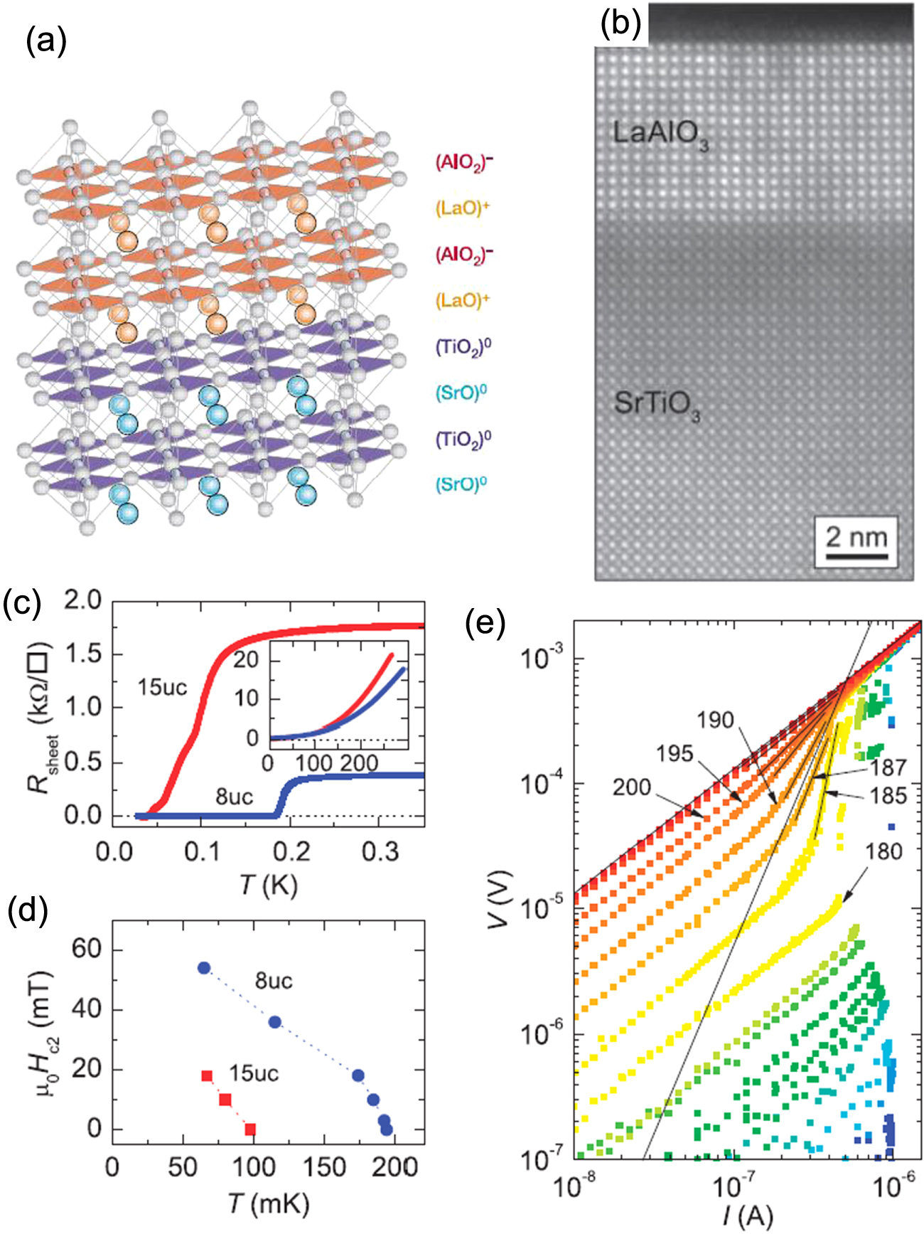
Figure 23. Superconductivity of CeCoIn5(n)/YbCoIn5(m) superlattices. (a) Temperature dependence of electrical resistivity ρ(T) for n = 1, 2, 3, 5, 7 and 9, compared with those of 300 nm thick CeCoIn5 and YbCoIn5 single-crystalline thin films. (b) Normalized Hc2(θ) of the n = 3 superlattice at 0.16 K and 0.8 K and of the n = 4 superlattice at 0.25 K and 0.9 K. (a) Reprinted by permission from Macmillan Publishers Ltd: Mizukami Y et al 2011 Nat. Phys. 7 849 [31], copyright 2011. http://dx.doi.org/10.1038/nphys2112. (b) Reprinted figure with permission from Goh S et al 2012 Phys. Rev. Lett. 109 157006 [195]. Copyright 2012 by the American Physical Society. http://dx.doi.org/10.1103/PhysRevLett.109.157006.
Download figure:
Standard image High-resolution image
Furthermore, anomalous behaviors were observed in the angular dependence of Hc2(θ), where θ is the angle of magnetic field relative to the in-plane direction [195]. When the conducting layers consisting of a quasi-2D superconductors are sufficiently decoupled, the angle dependence of Hc2(θ) obeys the 2D Tinkham model (see equation (9)) as long as the orbital pair-breaking effect is dominant. However, when Hc2(θ) is dominated by the Pauli paramagnetic pair-breaking effect, the angle dependence is expressed by the 3D anisotropic GL model regardless of the interlayer coupling strength (see equation (8)). In this case, the anisotropy of superconductivity reflects that of the g-factor in the Zeeman term. In [195], for n = 4, 5 (n: number of UCs for the CeCoIn5 layers), the angular dependence of Hc2(θ) was expressed by the 3D anisotropic GL model in a wide temperature range (see the lower panel of figure 23(b); the variation around θ = 0 is smooth). This was ascribed to the strong Pauli paramagnetic effect in CeCoIn5. For n =3, however, the angular dependence of Hc2(θ) at T = 0.8 K (Tc = 1.04 K) was described by the 2D Tinkham model (see the upper panel of figure 23(b); the variation around θ = 0 is cusp-like). This means that the orbital pair-breaking effect is stronger than the Pauli effect in this regime, considering the fact that the CeCoIn5 layers are well decoupled from each other. Therefore, it was concluded that a decrease in the layer thickness makes the Pauli effect weaker compared to the orbital effect. This phenomenon can be explained by the fact that the thinning of the CeCoIn5 layers leads to increasingly important roles of the CeCoIn5–YbCoIn5 interface and of the space-inversion symmetry breaking. Namely, the resultant manifestation of the Rashba effect significantly weakens the Pauli effect, because the spins are already polarized due the Rashba effect. Nevertheless, the Pauli effect was found to dominate again at lower temperatures (T ≪ Tc), which was interpreted as the effect of the FFLO phase appearing in CeCoIn5. The influence of the Rashba effect on Hc2(θ) was confirmed in a subsequent experiment, where additional space-inversion symmetry breaking was introduced by an asymmetric stacking sequence of CeCoIn5(n)/YbCoIn5(m)/CeCoIn5(n)/YbCoIn5(m') (m ≠ m') [196].
4. Summary
In the present review, we have seen that the existence of 2D superconductors with atomic-scale thicknesses have already been established in a wide range of fields and that they are now under extensive investigation from different viewpoints. The relevant superconducting materials encompass almost all categories: from simple elemental metals on semiconductor surfaces, graphene, transition metal chalcogenides, and FeSe, to more complex compounds and molecules such as cuprates, perovskite oxides, rare-earth based heavy-fermion systems, and organic conductors. This means that the degree of electron correlation, which is one of the key factors in the modern solid-state physics and materials science, ranges from the weak to the strong limit. In terms of experimental technique, the studies of 2D superconductors feature a large variety as well. For example, LT-STM/STS and ARPES are powerful tools for directly probing the superconducting energy gaps of atomically thin superconductors exposed to the surface. Their usage is not limited to the studies treated here, but they surely have great advantages because of their surface sensitivity. Highly advanced MBE and PLD techniques allow researchers to grow different kinds of heterostructures in a layer-by-layer fashion and to fabricate atomically well-defined interfaces and superlattices with ideal 2D characters. Two recent technical breakthroughs, the EDL-FET device and the mechanical exfoliation of atomic sheets, have also greatly activated and broadened the present topics. Undoubtedly, state-of-the-art nanotechnology, including the above examples, has been essential for studies on superconductors in the 2D limit and will surely continue to drive their developments in the coming future.
New phenomena and physics revealed in these systems are so diverse and significant that they are also worthwhile repeating here. Contrary to the general belief that superconductivity is fragile and must be suppressed as the material thickness approaches the atomic-scale limit, many 2D systems have been found to exhibit robust superconductivity at low temperatures as long as the structural and compositional quality of the sample is sufficiently high. This promises practical applications of these materials and devices in future. In some cases, the observed Tc is comparable to, or even higher than, that of the bulk counterpart, and, particularly for FeSe monolayers grown on SrTiO3 substrates, Tc is surprisingly high. Its origin is now under hot debate, but it is clear that the interface (or charge transfer through the interface) rather than the atomic-scale thickness itself plays the essential role. This may be called an interface-induced high-Tc superconductor, but the ultimately small layer thickness helps this effect manifest itself in a dramatic way. Aside from the Tc issue, there are many interesting phenomena and effects that take place, or are expected to do so, because of the two dimensionality and the presence of the interface. One of the examples is the formation of QWS, which leads to the Tc oscillation as a function of layer thickness and the Bean-like hard superconductivity. The absence of the usual orbital pair-breaking effect under in-plane magnetic field should lead to dominance of the Pauli paramagnetic pair-breaking effect. The signatures of the Rashba effect have already been detected in some materials, including Pb atomic layers and heavy-fermion compounds. The reduction of the layer thickness down to the half UC in transition metal dichalcogenides unveils the intrinsic inversion symmetry breaking of the lattices, from which the Ising superconductivity arises. In addition to these exotic phenomena, traditional themes such as the S–I transition have seen substantial progress, mostly thanks to the invention of the EDL-FET device. In some cases, new phases such as the Bose metal was indicated beyond the conventional theoretical framework of the S–I transition. Competition and coexistence of superconductivity with other many-body electronic states such as magnetism and CDW also enrich the physics and phenomena found in the regime of the 2D limit.
Although the studies on 2D superconductors with atomic-scale thicknesses have already been developed to a very high level, further important progress is sure to come in the next decade. This will be brought not only by focusing on individual topics described in section 3, but also by crossing their boundaries, i.e. by promoting the overlap among the categories shown in figure 1. Along the horizontal axis, different materials may be combined to fabricate 2D hybrid systems, for example, using organic molecules and metal atomic layers on semiconductor surfaces. In the vertical direction, different experimental techniques may be combined. For example, surface atom layers treated only in UHV so far may be investigated using an EDL-FET device after an appropriate protection process. The 2D superconductivity at the buried interface may be exposed to the surface for the purpose of LT-STM and ARPES studies. This certainly calls for an interdisciplinary approach involving material science, surface science, and device physics. In terms of new phenomena and physics, finding the topological superconductivity will be one direction to take, since combination of the conventional (BCS-type) superconductivity and the Rashba effect is one of the most promising methods for realizing it [197]. The two dimensionality is also a key factor in this respect, in view of observing and manipulating the Majorana zero mode within the vortex or at the edge [198, 199]. This may be an alternative approach in place of topological insulator-superconductor heterostructures, for which unusual vortex core states were observed by LT-STM [200, 201].
Acknowledgments
The author thanks A Tanaka, S Yoshizawa, T Yamaguchi, C Liu, Y Hasegawa, S Hasegawa, and H Weitering for fruitful discussions and their critical reading of the manuscript. This work was financially supported by JSPS KAKENHI Grants No. 25247053 /26610107 and by World Premier International Research Center (WPI) Initiative on Materials Nanoarchitectonics, MEXT, Japan.