
Abstract
Superconducting radiofrequency (SRF) cavities that could provide a higher quality factor as well as a higher operational accelerating gradient at an affordable cost are in high demand for the future generation of particle accelerators. This study aims to demonstrate the potential of Nb3Sn as material of choice for such SRF applications. Due to its brittle nature, the only way to produce an Nb3Sn SFR cavity is to synthesise a thin layer inside a cavity made of niobium or copper. In this work, direct current magnetron sputtering using a stoichiometric target of Nb3Sn was employed to produce films on copper samples. Assessment of the morphology, microstructure and superconducting properties were performed in order to ensure that this approach is suitable for SRF applications. The potential of the method is proven by obtaining films, which exhibit a crack-free surface, dense morphology and critical temperatures (Tc) up to 16 K. The essential properties of the films have also been investigated with respect to the deposition and annealing conditions. The use of krypton as working gas during deposition increases the atomic percent of Sn in the film compared to argon. However, in contrast to argon, higher krypton pressures reduce the atomic percent of Sn. It was also found that long-lasting high-temperature annealing leads to higher superconducting critical temperatures due to an increased crystallographic order. Particular attention was given to the influence of the copper substrate on the film growth as well as the microstructural and superconducting characteristics. We discuss the main constraints introduced by the copper substrate, such as copper interdiffusion during annealing, lattice mismatch and difference in thermal expansion coefficients and methods to overcome them.
Export citation and abstract BibTeX RIS

Original content from this work may be used under the terms of the Creative Commons Attribution 3.0 licence. Any further distribution of this work must maintain attribution to the author(s) and the title of the work, journal citation and DOI.
1. Introduction
The critical temperature twice as high as niobium and the high superheating field of Nb3Sn motivate the superconducting radiofrequency (SRF) community to develop methods to apply this material to accelerating cavities [1]. Nb3Sn cannot be used as a bulk material for cavity production due to its low thermal conductivity and brittle nature. Nevertheless, a thin film approach, in which a thin superconducting film is synthesised inside a cavity made out of an appropriate material, offers a promising route for exploiting Nb3Sn for SRF use. Two possible candidate substrate materials are niobium and copper. The usual choice of niobium as a substrate for synthesising the Nb3Sn layer is due to the wide spread use of this material for cavity production. The use of copper substrates, instead, could bring several advantages for operation when considering the higher thermal conductivity of copper at cryogenic temperatures and the cost reduction granted to the lower base material price. Copper has indeed proven its efficiency to stabilise superconducting niobium thin films, preventing thermal runaways [2–5].
Considerable attention has previously been applied to Nb3Sn films synthesis on niobium substrates. Starting from the 1970s, attempts to produce Nb cavities with a Nb3Sn layer grown using Sn vapour-phase diffusion were performed [6]. Similar encouraging results continued from the late 1980s up to the 2000s with several 1.5 GHz Nb and multi-cell cavities being prepared and investigated [7–9]. The main result of this analysis was cavities which had Q-values exceeding those of bulk niobium at 4.5 K and low accelerating fields but which exhibited a strong Q-drop beyond a peak field of 15–30 MV m−1. After several years of interruption, different groups resumed the study using modified vapour diffusion methods [10, 11]. Even making use of this new manufacturing method, problems associated with the Q-slope and early quenching remained unsolved. One possible cause for this behaviour was identified as the non-uniform thickness of the Nb3Sn layer and the non-uniform Sn distribution over the cavity surface [12]. However, it should be noted that these Nb3Sn preparation techniques are not applicable when a copper substrate is used, because of the processing temperature that is higher than the melting point of copper.
One of the interesting alternatives that can be used to synthesise Nb3Sn on substrates other than niobium, is electrodeposition from SnCl2 and NbCl5 in 1-butyl-3-methylimidazolium chloride ionic liquids. This approach allows Nb3Sn to be formed on a copper substrate in molecular form without high-temperature treatment [13]. A combination of electrodeposition of Sn with Cu intermediate layers and thermal treatment has also previously been used to deposit Nb3Sn on niobium substrates [14]. The layer elaborated with such technique still needs to be tested under RF field especially to assess the potential effect of undesired crystalline phases, such as NbSn2, observed by x-ray diffraction (XRD) analysis. In addition a recipe should be defined for the removal of the topmost bronze layer.
An alternative manufacturing approach is direct current magnetron sputtering (DCMS), which has been used to produce high-quality Nb3Sn thin films on a range of substrates. Most of this development has been directed towards sapphire substrates, where the potential of this method has been revealed through films exhibiting a critical temperature from 15.3 to 18.3 K [15–18]. The principal advantages of the method are its simplicity and the possibility to produce homogenous layers of Nb3Sn on complex shapes. However, the DCMS synthesis of Nb3Sn films on a copper substrate brings additional challenges. For example, the difference in thermal expansion coefficients between the Nb3Sn film and substrate contributes to disorder and thereby the critical temperature of the film, as shown by Kampwirth et al [17], is lowered by 5 K compared to the equivalent films grown on sapphire substrate.
DCMS has been extensively used to produce niobium thin film coated accelerating cavities for several accelerating facilities as LEP, LHC, HIE ISOLDE at CERN, ALPI (INFN, LNL, Italy), and SOLEIL (St-Aubin, Gif-sur-Yvette, France) or ELETTRA and SLS for third harmonic bunch lengthening accelerators [2–5]. These previous successful transitions from test samples to real elliptical and quarter wave cavities justify the continued development of this approach for the production of Nb3Sn films.
In the present work, DCMS has been employed to synthesise Nb3Sn films on copper samples. Two different thermal treatment routes are proposed to produce these films, one in situ and the other which is applied after the coating procedure. We then investigate the effect of prolonged heat treatment on the superconducting critical temperature of the films. The effect of the copper substrate and the impact it has on thin film growth are also discussed. Finally, the substantial impact of the microcrystalline strain on the final superconducting performance of the film is demonstrated.
2. Sample preparation and characterisation
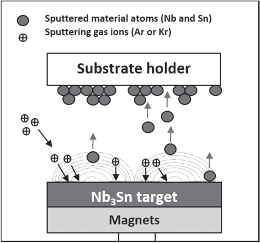
Thin films of Nb3Sn with thicknesses ranging from 1.5 to 2 μm were grown on copper substrates using a planar DCMS system with a niobium–tin stoichiometric target. A schematic image of the sputtering setup is presented on figure 1.

Figure 1. Schematic image of the sputtering setup.
Download figure:
Standard image High-resolution imageOxygen-free electronic grade copper substrates were chemically polished for 20 min in a mixture of sulfamic acid (H3NO3S, 5 g l−1), hydrogen peroxide (H2O2, 5% vol), n-butanol (5% col) and ammonium citrate (1 g l−1) at 72 °C before being loaded into the deposition chamber. Ar and Kr were used as sputtering gases at coating pressures ranging from 1 × 10⁻³ to 5 × 10⁻² mbar and from 3 × 10⁻⁴ to 3 × 10⁻² mbar, respectively. A power applied during the coatings of 200 W, distance between sample holder and cathode of 100 mm and 1 h coating duration were used for all samples. The gas type and coating pressure were adjusted to control the composition of the Nb3Sn films. This is of primary importance for A15 phase formation, as the production of an A15 lattice structure without the presence of pure niobium, tin or undesired phases of Nb–Sn, (such as Nb5Sn6 and NbSn2) is only possible in the very narrow region of compositions ranging from ∼19 to 26 at Sn% [19]. This lead to adopt a stoichiometric target.
To form the A15 superconducting phase, the films must undergo a high-temperature treatment; two different approaches were investigated. The first approach was based on annealing the films after the coating; it will be referred to as 'reacted AFTER coating'. The annealing temperature applied to the film needs to be sufficiently high to facilitate A15 phase formation, however it cannot exceed the melting temperature of copper or damage the flanges which are brazed at 830 °C. Therefore, the investigated temperature range was selected to be from 600 °C to 800 °C, with durations of between 24 and 72 h. Annealing was performed in a vacuum furnace with a base pressure of ∼10−6 mbar during the treatment, a temperature uniformity of ±3 °C and a ramp rate of 300 °C h−1. Following the annealing process, the samples were left inside the closed furnace to cool to room temperature.
The second investigated thermal processing route was the use of hot substrates during DCMS, which will be referred to as, 'reacted DURING coating'. Films were coated using substrate temperatures between 600 °C and 735 °C and the same coating parameters as for 'reacted AFTER coating' method. Two thermocouples monitored the temperatures of the sample holder and resistive heater during the entire process. In some cases, samples synthesised using this approach were subsequently annealed either in the high-vacuum furnace described above or directly in situ by keeping the samples at a high temperature without venting to the air the coating system.
The composition of the films was determined using energy-dispersive x-ray spectroscopy (EDS). Measurements were carried out on each sample on five randomly selected sites within a 200 μm × 200 μm area using an accelerating voltage of 10 kV. The aperture has been adjusted to maximise the acquisition rate with minimum acquisition of 106 total counts per spectra for each sample. For some samples, x-ray photoelectron spectroscopy (XPS) was applied to obtain more detailed elemental quantification of the surface. Analysis was performed at normal emission angle on the surface of the samples and after removing by argon sputtering approximately 2.5 nm of the material using XPS setup with a XR50M M x-ray AlKα monochromatized source and a PHOIBOS 150 hemispherical energy analyser equipped with nine channeltrons from SPECS GmbH.
Surface morphologies of the coated Nb3Sn films before and after high-temperature treatment were investigated using scanning electron microscopy (SEM). A Zeiss Sigma field emission gun SEM equipped with an InLens detector (Secondary Electron), an Evan-Thornley secondary electron detector and an angular selected backscattered detector was used for imaging. To examine the cross section of the films and elemental distribution within the film and near surface copper, a ZEISS 'XB540' focused ion beam (FIB) was used. For the cross sectional milling, Pt deposition was initially performed at a milling current of 300 pA and an accelerating voltage of 30 kV to deposit 1 × 3 × 15 μm3 protection barrier. Coarse milling at a current of 7 nA and accelerating voltage of 30 kV was then used to remove a 5 × 7 × 20 μm3 region of material, before the cross sectional surface was polished at a milling current of 300 pA.
In order to facilitate elemental mapping at the required nanoscale resolution transmission EDS was performed on transmission electron microscopy (TEM) lamella of the films. These were produced by initially milling a cross section into the sample using the conditions outlined above. A similar milling process was then used to cut a 3 μm section of material which was removed from the surface using a micromanipulator, before being mounted on a copper grid. Sequential polishing was then used to reduce the thickness of the lamella to less than 200 nm, with a final milling current of 50 pA and accelerating voltage of 5 kV.
A Siemens D5000 diffractometer employing Cu Kα radiation was used to perform XRD on the samples at a voltage of 40 kV and current of 35 mA. For characterisation of the phases diffraction patterns were obtained in Bragg Brentano geometry in coupled θ/2θ configuration, and by making use of a Ni filter in the diffracted beam.
Diffraction patterns were also obtained to provide insight into the atomic strain behaviour by making use of a parallel plated collimator and a LiF [100] monochromator. A grazing angle incidence/2θ detector scan configuration was implemented, with grazing angle fixed at 7° and a detector scan 2θ range of 30°–150°. The scan step size was 0.02° and the time spent on collecting the data per step was 16 s. Calibration of the instrumental function was determined using a LaB6 powder.
The capabilities of XRD analysis are not limited to the identification of the phases present in the sample but provide considerable information on the changes in the lattice structure of the thin films.
In order to evaluate microstructural parameters, the software MAUD was used to perform Rietvelt refinement of the diffraction patterns [20–24]. An isotropic microstructural model was used to estimate the average crystallite sizes for the samples reacted after and during coating, and rms microstrains from the diffraction peak profiles for samples reacted after the coating.
The superconducting critical temperature of the Nb3Sn films was measured using a vibrating sample magnetometer (VSM-SQUID). The VSM-SQUID system is equipped with a superconducting coil able to generate magnetic fields up to 7 T and the sample temperature can be regulated between 1.8 and 400 K. Specimens of dimension 4 × 4 mm2 were cut for critical temperature testing from the copper samples using electro-spark erosion in oil. Each sample was zero-field cooled before measurement. To get rid of the residual flux possibly trapped in the superconducting coil, the latter was quenched before starting the zero-field cooling procedure. For comparison, some films of Nb3Sn were also grown on ceramic substrates (Al2O3), and the superconducting critical temperatures of these samples were obtained using four point probe resistance measurements.
3. Results and discussion
3.1. 'Reacted AFTER coating' process
As mentioned above, the primary composition adjustment parameter during the coating process was the process pressure. In figure 2 the dependence of the Sn atomic percent in the Nb3Sn films as-deposited versus coating gas pressures using either Ar (closed circles) or Kr (open circles) is shown. Atomic Sn percentage for the samples reacted AFTER the coating varies from ∼21% to ∼27%, still in the suitable range according to the Nb–Sn phase diagram [19]. To control Sn distribution along cathode diameter of 150 mm, long copper stripes with length equal to the cathode diameter were coated at four different working pressures and analysed. Composition over the stripes length varies withing 1–2 at%.
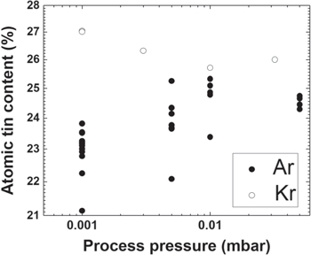
Figure 2. Nb3Sn films composition with respect to coating pressure using either Kr (open symbols) or Ar (closed symbols) as a sputtering gas.
Download figure:
Standard image High-resolution imageDeposition using Kr provides an increase of Sn at% up to ∼3 at% compared to Ar. While using argon as the process gas, an increase of gas pressure rises atomic Sn percentage in the coated Nb3Sn films, the use of Kr gas shows an opposite behaviour with a decrease in the atomic tin content in the film for increasing deposition pressures.
Post-coating annealings with various temperatures were applied to the deposited Nb3Sn films to promote the formation of the superconducting A15 phase.
As it was observed, the annealing process can cause slight Sn evaporation for the films coated at deposition pressures up to 1 × 10⁻² mbar, but such deviation in the composition is not sufficient to interfere with superconducting A15 phase formation during annealing.
Nevertheless, Sn losses become significant for the samples coated at high coating pressures (∼5 × 10⁻² mbar and higher), where the annealing process is causing nearly complete Sn evaporation during the heat treatment, and formation of superconducting A15 phase becomes impossible. These samples were excluded from further characterisation.
Witness bulk niobium pieces were annealed together with Nb3Sn samples and then analysed using XPS analysis to confirm Sn evaporation. Traces of Sn were observed on the surface of the Nb samples after high-temperature treatment. To prevent this problem in future applications annealing could be performed in a closed configuration for cavities.
In figure 3, typical XRD diffractograms for the Nb3Sn films deposited at an argon pressure of 1 × 10⁻³ mbar as-deposited (a) and after annealing for 24 h at 700 °C under vacuum (b) are shown.

Figure 3. XRD analysis performed for the sample 'reacted AFTER coating' as-deposited (a) and (b) after annealing.
Download figure:
Standard image High-resolution imageXRD analysis of the samples before and after annealing confirms the formation of superconducting A15 phase only after high-temperature treatment. The expected diffraction pattern lines and their relative intensities are represented in red up-pointing triangles for Cu and blue circles for the Nb3Sn phase. As-deposited Nb3Sn films do not exhibit the superconducting A15 phase: the diffractogram (figure 3(a)) suggests a layer either amorphous or nanocrystalline according to the low intensity and broad peak (110) of Nb3Sn (insert in figure 3(a)). Diffraction peak at 68° could suggest the presence of nanocrystalline Nb or Nb6O that cannot be disentangled at this stage of the study. The presence of characteristic peaks of Nb3Sn shown with blue circles (figure 3(b)) confirms the A15 phase formation after high-temperature treatment.
The crystallites' size of Nb3Sn films reacted after coating was estimated within the range of ∼70–190 nm using Rietveld analysis, which is in good agreement with surface SEM observations.
The coating and annealing conditions strongly influence surface morphologies of the films. As an example, figure 4 displays the SEM surface images of typical Nb3Sn films as-deposited (a), (c) and after annealing for 24 h at 800 °C (b), (d) coated under Ar (a), (b) and Kr (c), (d) atmospheres with a pressure of 1 × 10⁻³ mbar.

Figure 4. Morphology of Nb3Sn films grown on copper substrates using Ar (a), (b) and Kr (c), (d) as deposition gas—as-deposited (a), (c) and after annealing at 800 °C for 24 h (b), (d). The scale bars represent 200 nm.
Download figure:
Standard image High-resolution imageBoth films synthesised under Ar and Kr gas pressures are highly disordered as-deposited, while annealing causes the formation of a grainy pattern. A difference in structural properties of the films coated with a different working gas can also be observed after heat treatment. In figure 5 one can see that samples coated under Ar pressure show cracks on the surface after the annealing step while films coated using Kr exhibit a crack-free surface.
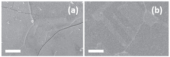
Figure 5. Surface morphology of Nb3Sn coated under 1 × 10⁻³ mbar of (a) Ar and (b) Kr atmosphere after high-temperature treatment. Scale bars represent 400 nm.
Download figure:
Standard image High-resolution imageIncorporated argon could contribute to the increase of residual stresses in the film and cause cracking during the annealing step. In films produced using the DCMS system some control of discharge gas trapping is needed to fine-tune the properties of the films [25]. The quantity of incorporated gas during deposition strongly depends on the relation between the atomic masses of the discharge process gas, and the cathode sputtered material [26]. The choice of deposition gas could influence the gas content in the produced samples. As it was shown in [26], Kr content in the film is expected to be lower than Ar. This point is currently under investigation through the measurement of the residual gas content and residual stresses in the different coatings.
3.2. 'Reacted DURING coating' process
Nb3Sn films reacted during the coating were considered as an alternative way to achieve a stable superconducting A15 phase in the samples. As in the case of samples 'reacted AFTER coating' the nature of the sputtering gas, as well as its pressure during coating, were chosen as the mean to optimise the composition and morphology of the synthesised structures. In figure 6 the dependence of tin content versus coating pressure is presented: films coated using Ar as working gas are shown with black circles, samples coated with Ar and kept at a high temperature for five additional hours are presented with black stars, and open symbols represent samples produced with Kr as sputtering gas.

Figure 6. Composition of Nb3Sn films reacted during coating with respect to the coating pressure using either Kr (open symbols) or Ar (closed symbols) as a sputtering gas.
Download figure:
Standard image High-resolution imageThe tin content in the samples produced using this route varies between ∼19 and 25 at%. Most of the samples were synthesised using Ar as a deposition gas, and some trials were made using Kr.
XRD analysis confirms the presence of superconducting A15 phase for all samples reacted during coating at all investigated temperatures.
Typical XRD diffractogram for a sample coated at 710 °C under Ar pressure of 1 × 10⁻³ mbar is presented in figure 7. Nb3Sn characteristic peaks confirm the formation of the superconducting cubic phase in the film. The crystallite sizes of Nb3Sn films reacted during coating, calculated using the Rietveld method are significantly larger than for the films reacted after the coating and exceed the limit values of the method (>400 nm).

Figure 7. XRD diffractogram for a sample coated at 710 °C under Ar pressure of 1 × 10⁻³ mbar.
Download figure:
Standard image High-resolution imageIf the nature of the sputtering gas does not significantly affect the morphology of the films figure 8(a), its absolute pressure seems to have a substantial impact as presented in figure 8(b).

Figure 8. Morphology evolution of the Nb3Sn films with different coating and annealing parameters. The scale bars represent 200 nm.
Download figure:
Standard image High-resolution imageNb3Sn films deposited under low deposition pressures tend to produce films with dense, relatively smooth surface morphologies and at the same time exhibit a lower Sn content. On the contrary, high coating pressures increase the Sn content but lead to a rougher surface. During higher gas pressure coatings, sputtered material atoms suffer more collisions with the process gas atoms and lose substantial kinetic energy, resulting in a randomly oriented structure with more voids and rougher structure. We assume that a low coating pressure, close to 1 × 10⁻³ mbar, is the most appropriated one for SRF application as the final surface is smoother and thus less prone in providing field emitting features during cavity operation.
On top of the pressure, the coating temperature strongly affects the final film morphology as shown in figure 8(c). Bigger crystalline structures are obtained at a high temperature thanks to the enhanced adatoms' surface mobility. Finally keeping the film at a high temperature for several hours once the coating process is ended allows to further modification of the film morphology. The latter results in a clear growth of the crystalline structures suggesting that the coating duration is not long enough to reach a stable phase and that additional time is needed to let the film reaching an equilibrium. More detailed analysis of the surface morphologies using TEM is foreseen in order to assess the nature of the black dots presented at SEM pictures in figure 8(a) which from our first investigation look like to be topological features.
3.3. Superconducting properties
The low temperature magnetic properties of the samples grown on copper substrate were investigated using VSM-SQUID.
A typical dependence of magnetic moment versus temperature is presented in figure 9.

Figure 9. Magnetic moment versus temperature at B = 12 Oe (sample zero-field cooled) for the sample reacted after coating and annealed under vacuum atmosphere for 24 h at 750 °C. The inset shows the temperature derivative of the magnetic moment as a function of the temperature.
Download figure:
Standard image High-resolution imageValues of the critical temperature Tconset were extracted from the transition point of the diamagnetic region with a negative moment (superconductivity) to the paramagnetic region with positive values of magnetic moment (normal conductivity region). We decided to focus on the onset value as it highlights the maximum reachable critical temperature for a given sample. Further optimisation will be carried out in order to minimise the transition width, which is most likely due to unreacted material, uneven composition distribution in the sample, contamination of the film or disorder in the crystalline lattice. It is to be noted that the transition broadness was observed to vary between 0.4 and 5 K with an average value of (1.7 ± 1.4) K.
The best obtained critical temperature for Nb3Sn samples grown on copper substrate is around 16 K which remains 2 K below the expected theoretical bulk value of 18.3 K.
In figure 10(a) the dependence of the critical temperature onset on tin content in the films as-deposited is shown and compared with bulk Nb3Sn (black triangles) [27]. Films coated using both routes reacted after and during coating are shown as blue squares and red circles, respectively.

Figure 10. Critical temperature versus tin percentage. Black triangles represent reference data for bulk Nb3Sn [27]. Circles and squares are the experimental points for samples reacted during and after the coating respectively. (b) Diamonds are attributed to samples of identical composition without (half-filled) and with (full) post-coating annealing.
Download figure:
Standard image High-resolution imageAs was discussed in many works, superconducting properties of the A15 material, i.e. critical temperature, critical current density, upper critical field are in correlation with the long-range crystallographic order (LRO) of the lattice [27–29]. Theoretically, bulk Nb3Sn with nominal stoichiometry at low temperature would have the highest possible crystallographic order [30]. In real structures, some disorder may remain in the lattice due to the finite time of cooling down from the melt or applied annealing [30]. In the case of thin films, this is complicated by additional disorder introduced both during deposition and during applied thermal treatment. Deviation from stoichiometry, which causes crystallographic disorder in the A15 phase, leads to lower critical temperature values as can be seen in figures 10(a), (b).
Some previous works on A15 materials have shown that crystallographic order might be destroyed by high-energy neutron radiation and almost completely recovered by annealing [31]. We observed a similar effect of the annealing on critical temperature for the Nb3Sn films reacted during coating. In figure 10(b), two samples marked with red diamonds were coated using the same deposition parameters. The use of post-coating annealing for 57 h to one of the samples allowed increasing its critical temperature by more than 3 K and achieving Tc close to the critical temperature of bulk Nb3Sn with the same composition.
The effect of the high-temperature treatment duration can be considered by comparing films reacted after and during coating with the same composition (see dashed lines in figure 10(a) at Sn at% ∼22.9 and Sn at% ∼23.7). These points indicate that the critical temperatures for samples reacted during coating are lower compared to samples reacted after annealing. In the case of the films reacted during coating, substrates are heated only during the deposition time, i.e. ∼1 h, while post-coating annealing for the films reacted after coating takes ∼24 h. We believe that the rise of the annealing time increases the LRO degree and, hence, Tc.
3.4. Influence of microstrain on the superconducting properties
XRD is a robust method to perform quantitative characterisation of microstructural properties of the films. XRD measurements and details of the Rietveld refinement analysis are described above.
In this study, only samples coated under Ar pressure were taken into consideration. In figure 11 microstrain versus critical temperature dependence calculated for the samples reacted after annealing is shown.

Figure 11. Critical temperature versus microstrain values for 'reacted after coating' Nb3Sn films.
Download figure:
Standard image High-resolution imageAll these films shows cracks after annealing, thus uniform residual stress is released, but microstrain, a non-uniform strain that varies on a microscopic scale, remains significant.
This critical temperature sensitivity from microstrain confirms the importance of the microstructural properties for superconducting properties of the Nb3Sn films. In the case of films reacted during coatings no direct correlation could be found between the microstrain and the critical temperature. However it is very likely that in this case the residual stress effect surpasses the microstrain one. Further investigation are now needed to disentangle the effect of stresses and microstrain on the final reachable critical temperature.
3.5. Copper substrate influence
The use of copper as substrate requested a detailed study of its influence on the structural and superconducting properties of the sputtered Nb3Sn films. The impact of the copper substrate can be seen in figure 10 where Nb3Sn films grown on copper compared to the reference data of bulk Nb3Sn systematically exhibit lower critical temperature at given composition.
Nb3Sn films were grown both on copper and Al2O3 ceramic substrates using the same deposition parameters to separate the impact of magnetron sputtering film synthesis from that of the copper substrate in disorder degree.
The influence of the substrate choice on critical temperature values can be seen in table 1, which brings into comparison two pairs of films grown on copper and ceramic substrates using identical coating parameters, i.e. argon pressures of 1 × 10⁻³ and 5 × 10⁻³ mbar. After the coating, all samples were annealed at 750 °C for 24 h.
Table 1. Influence of the substrate on critical temperature of the Nb3Sn films.
| Critical temperature (K) | ||
|---|---|---|
| Process pressure | Copper substrate | Ceramic substrate |
| P = 1 × 10⁻³ mbar | 14.7 K | 17.5 K |
| P = 5 × 10⁻² mbar | 15.5 K | 17.4 K |
The impact of the copper substrate manifests itself in lower critical temperature values by ∼2–3 K.
On top of the critical temperature depression caused by copper substrate the difference in thermal expansion coefficient jointly with the brittleness of Nb3Sn lead to surface cracking after annealing in films reacted after coating. Undesired for RF applications, crack formation could be avoided by a careful optimisation of the deposition parameters, including the substrate choice, and of the annealing parameters.
Another essential problem of the copper substrate associated with long-lasting annealing treatments is copper interdiffusion into the Nb3Sn layer.
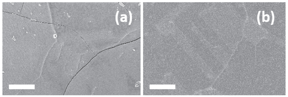
In figure 12(b) EDS mapping of copper on a cross section of Nb3Sn film reacted after coating is presented. Boundaries of the film as well as copper-rich regions are highlighted.

Figure 12. SEM image (a) and copper elemental mapping of Nb3Sn film (b) reacted after coating. Scale bars represent 1 μm.
Download figure:
Standard image High-resolution imageElemental mapping was performed on FIB cross section of a Nb3Sn film. The analysis reveals nano-to-microscale copper inclusions towards the upper surface of the thin film.
In case of high-temperature depositions, copper interdiffusion into the superconducting layer manifest itself differently in films synthesised using Ar or Kr as working gas. Films prepared with Kr reveal copper-rich features (up to ∼10 at%) observed on the surface of the produced Nb3Sn films, as it can be seen in figure 13.

Figure 13. Surface morphology of Nb3Sn film deposited using Kr as a sputtering gas. Scale bar represents 2 μm.
Download figure:
Standard image High-resolution image
SEM-EDS analysis of the films coated with Ar, did not detect any copper inclusions inside Nb3Sn layer as in case of reacted after coating films (figure 12) or copper-rich features on the surface as in case of the films grown under Kr pressure, which can be seen (figure 13). However, additional XPS analysis on the surface of the film detected traces of copper up to 7 at%.
For SRF applications, the presence of copper in the superconducting Nb3Sn layer is undesired, as it creates local non-superconducting spots which would lead to power dissipation during the cavity operation and thus to poor performances. An appropriate intermediate layer between copper and Nb3Sn could be a good response to the challenges caused by the copper substrate. Choosing a material with similar thermal expansion coefficient could increase the LRO degree, with consequent critical temperature increase, as well as reduction of residual stress in the superconducting film, which could prevent cracking of the films during annealing. Diffusion properties of the material together with the proper thickness of the intermediate layer could help to mitigate copper interdiffusion to the Nb3Sn film. Several possible materials are currently under investigation.
4. Conclusion
We performed an extensive characterisation of Nb3Sn thin films grown using a magnetron sputtering system. Thin films with critical temperatures up to 16 K are synthesised onto polycrystalline copper. We established the dependence of the deposition and annealing parameters on the superconducting and microstructural properties of the produced films. Deposition gas type and pressure affect the composition of the films with the latter ranging from 20% to 27% Sn content. High Ar pressure leads to a higher Sn atomic content in the structures, but at the same time causes rough and more porous morphology. The use of Kr as deposition gas also leads to an Sn content increase when compared to Ar, but an increase in Kr pressure decreases the Sn content in the film. Different high-temperature regimes are responsible for the superconducting and microstructural changes. Treatment with higher temperatures and durations increase the crystallographic order degree and hence, critical temperature. When compared to the ceramic substrate the effect of copper is demonstrated in decreasing the actual critical temperature of the film. Based on the present study, we believe that for the moment the most promising method for the future SRF application is high-temperature magnetron sputtering at low argon pressure, which gives dense films morphologies desired for SRF. To achieve composition close to stoichiometric, the pressure is chosen to be 5 × 10⁻³ mbar. The lower critical temperature of the samples reacted during coating compared to films reacted after the sputtering can be compensated by the subsequent annealing at ∼750 °C for 24 h or longer. The use of an intermediate layer between copper and Nb3Sn is envisaged to overcome problems due to the use of a copper substrate.
Acknowledgments
The research leading to these results has received funding from the European Commission under the FP7 Research Infrastructures project EuCARD-2, grant agreement no.312453. The research leading to this document is part of the Future Circular Collider Study. We thank the group of applied superconductivity in Geneva University, i.e. C Senatore and M Bonura, who performed the SQUID VSM measurements. The authors also thank the surface treatment team of CERN who performed all the samples chemical preparation prior to coating as well as H Neupert and D Zanin for the XPS analysis.