
Abstract
Attosecond science is based on electron dynamics driven by a strong optical electric field and has evolved beyond its original scope in gas-phase atomic and molecular physics to solid-state targets. In this review, we discuss a nanoscale attosecond physics laboratory that has enabled the first observations of strong-field-driven photoemission and recollision at a solid surface: laser-triggered metallic nanotips. In addition to the research questions of rather fundamental nature, femtosecond electron sources with outstanding beam qualities have resulted from this research, which has prompted follow-up application in the sensing of electric fields and lightwave electronics, ultrafast microscopy and diffraction, and fundamental matter-wave quantum optics. We review the theoretical and experimental concepts underlying near-field enhancement, photoemission regimes and electron acceleration mechanisms. Nanotips add new degrees of freedom to well known strong-field phenomena from atomic physics. For example, they enable the realization of a true sub-optical-cycle acceleration regime where recollision is suppressed. We also discuss the possibility of high-harmonic generation due to laser irradiation of metallic nanostructures.
Export citation and abstract BibTeX RIS

Original content from this work may be used under the terms of the Creative Commons Attribution 3.0 licence. Any further distribution of this work must maintain attribution to the author(s) and the title of the work, journal citation and DOI.
1. Introduction and early developments
The discovery of the surprisingly efficient generation of high-harmonic radiation from atomic gases (McPherson et al 1987, Ferray et al 1988) has led to the invention and broad acceptance of the recollision picture, which is at the core of the so-called simple man's model or three-step model. While its origins date back about 30 years (Kuchiev 1987, Gallagher 1988, van Linden and van den Heuvell 1988), the model was widely accepted about 25 years ago when a number of papers appeared (Corkum 1993, Schafer et al 1993, Becker et al 1995). It is thus appropriate to celebrate the 25th anniversary of the recollision picture with this special issue. Since then, several new and quite spectacular research fields have grown out of the initial discoveries, which originated in the realm of high-field atomic physics but have now reached out into various other disciplines (see Calegari et al (2016) for an overview of recent developments). Examples include the efficient generation of coherent extreme ultraviolet (XUV) and even x-ray pulses, the generation of attosecond light pulses, electron diffraction experiments with the electrons emitted from the irradiated atoms, molecules and clusters, and strong-field and recollision physics in condensed matter. In this contribution, we provide a review on this last topic, namely strong-field and recollision physics at the surface of nanoscale solids. Aspects of this research are reflected in a number of reviews and books (Vasa et al 2009, Krüger et al 2012a, Hommelhoff and Kling 2015, Jones et al 2016, Ciappina et al 2017). The focus of our review will be on a particular nanostructure geometry: sharp metallic needle tips.
We will recapitulate how three well-established fields came together to merge into a new field, offering new insight and applications alike: (1) a century of experience in field emission from needle tips, (2) atomic recollision physics, and (3) nano-optics, also known as near-field optics. This combination enables an unprecedented confinement of light–matter interaction to nanometer length and attosecond time scales.
1.1. Overview and structure
In the following part of the introduction (section 1.2), we will review early work on needle tips and strong-field photoemission from solids. Because nano-optics is of high importance for strong-field physics at needle tips, we will discuss it in greater detail in Chapter 2. Chapter 3 deals with experimental methods that have been used to elucidate the many open questions around the merger of gas-phase strong-field physics with solid-state systems. In Chapter 4, we discuss photoemission mechanisms, the in-depth understanding of which is not only important in its own right but for realizing new ultrafast and coherent electron sources. In Chapter 5, an overview is given of theoretical methods that are frequently used for the modeling of strong-field physics at metal tips. Temporal dynamics of the emission processes is discussed in more detail in Chapter 6, while prototypical strong-field effects, namely the acceleration and recollision of photoelectrons by the waveform of the driver field, are reviewed in Chapter 7. Modulating the waveform enables the control of strong-field photoemission and acceleration, as discussed in Chapter 8. Chapter 9 explores the feasibility of high-harmonic generation (HHG) at nanotips and presents the first ab initio results. In Chapter 10, we give a brief overview of the wide range of applications of the observed strong-field phenomena at needle tips, before concluding our review in Chapter 11.
1.2. Early work
Sharp metal needle tips have already been used for more than 80 years, even before the pioneering works of Erwin W Müller (Müller 1936), as excellent electron sources in various applications. The electron beam emitted from such a tip, in particular in cold field emission mode, is extremely bright and coherent, which is the reason it is routinely used in high-resolution electron microscopes, even though the easier-to-operate Schottky sources are nowadays preferred despite their slightly inferior performance (Spence 2013). A highly coherent electron beam can be generated in DC operation when a strong static negative electric field is applied to a metal tip. Because of the accumulation of field lines at the tip apex, the potential landscape in the vicinity of the apex is changed so that electrons can tunnel through the potential barrier from the metal to the vacuum side. This is the well known field emission process, requiring static field strengths in excess of 1 GV m−1 to observe a measurable electron current from a typical metal.
Nonlinear photoemission, in particular the two conceptually identical processes of above-threshold ionization of atoms and above-threshold photoemission from solids, represents the foundation on which strong-field physics stands. We recall early work on laser-driven (multi-) photon–electron emission from solids, before we go in medias res. With 'early' we refer to work published before the three 2006/2007 papers, which can be considered the first report on coherent electron sources driven by ultrafast photoemission processes (Hommelhoff et al 2006b, 2006c, Ropers et al 2007c). Subsequent papers provided clear evidence of strong-field physics at metal tips (Bormann et al 2010, Schenk et al 2010).
Multiphoton photoemission from metals dates back to the seminal work by Keldysh in 1965 (Keldysh 1965). In the same year, Keldysh's method was applied to metals by Bunkin and Fedorov, who, in essence, showed that the limiting cases are DC field emission in the low-frequency limit and multiphoton physics for high frequencies (Bunkin and Fedorov 1965), closely mirroring analogous concepts in atomic physics.
On the experimental side, the invention of the laser quickly led to the discovery of nonlinear photoemission; two-photon photoemission from solids was first observed in 1964 at a semiconducting Cs3Sb photocathode (Sonnenberg et al 1964). In Budapest, Farkas and colleagues investigated higher-order nonlinear photoemission early on with picoseond laser pulses (Farkas et al 1971, 1972, Farkas and Chin 1985), referring to Keldysh's theoretical work. Clear deviations from perturbative multiphoton emission and the onset of optical tunneling effects in electron emission from a gold surface were reported in 1991 (Tóth et al 1991).
In parallel, the photofield emission process was investigated and later utilized for inferring the band structure of metals. Here, an electron is photo-excited inside the metal close to or below the emission threshold, and then undergoes field emission (Lee 1973, Radoń 1998). Because field emission is exponentially sensitive to the barrier height, a current measurement as a function of the applied DC voltage allows the identification of the origin of the electrons; this, in combination with the known but variable photon energy, enables a reconstruction of the band structure of the metal under scrutiny.
While the well-defined excitation of electrons (from close to the Fermi level) to a well-defined intermediate state is the basis of photofield emission spectroscopy, the (laser-pulse-induced) heating of the electron gas inside a metal tip also leads to enhanced electron emission rates (Lee et al 1980, Riffe et al 1993). Hence, spectral information of the emitted electrons is mandatory to obtain a clear picture of the emission process and its dynamics. In particular, the question arises whether the participating electrons thermalize before they are emitted, or whether the electrons are emitted coherently as indicated by photon orders showing up in the spectra. However, an unstructured spectrum does not necessarily imply that the emission is thermal and incoherent, as photoemission studies from flat metals are prone to focal averaging effects. Focal averaging implies that electrons emitted in various regions of the laser spot experience different peak laser field strengths leading to a smeared-out electron energy distribution, to the extent that photon orders are no longer discernible. Yet another effect often arising in photoemission in the high-intensity regime from flat metal surfaces can wash out photon orders, namely space-charge repulsion within the emitted electron cloud. The reader is referred to earlier work on flat metal surfaces, for example, to Aeschlimann et al (1995), Damascelli et al (1996), and to Gault et al (2007), Kealhofer et al (2012) for more recent work on metal needle tips.
Two-photon photoemission (2PPE), in particular time-resolved 2PPE, is the method of choice for inferring various (often electronic) time scales in metals. It has strong ties to strong-field physics at metal surfaces, given the fact that this method allows the measurement of electronic processes on the femtosecond scale. We will not discuss this broad research field further, but refer the reader to two reviews (Petek and Ogawa 1997, Bauer et al 2015).
Laser pulses with sub-picosecond duration are necessary for these studies to reach the nonlinear photoemission regime without inducing damage to the sample. The large deviation of the electron temperature from the lattice temperature on sub-picosecond time scales is indeed important for explaining the observed emission behavior in photoemission experiments with sub-picosecond pulses (Riffe et al 1993, Girardeau-Montaut and Girardeau-Montaut 1995).
Long before the recollision picture had been introduced, above-threshold ionization had been observed from atoms (Agostini et al 1979, Kruit et al 1981), where many photon orders could be unequivocally identified in photoionization spectra. Similarly, shifting of the multiphoton peaks because of field effects, in particular the AC Stark effect and the role of the ponderomotive potential, had been well understood through experiments from atoms in the gas phase (Kruit et al 1983, Muller et al 1983, Bucksbaum et al 1987). Some ten years later, indications of the counterparts in photoemission from solids had been reported: above-threshold photoemission (ATP) including potential ponderomotive effects initially in the late 80s (Luan et al 1989, Fann et al 1991, Farkas et al 1993) and later more clearly (Banfi et al 2005, Bisio et al 2006). Notably, well-defined photon orders could be observed, and the prevalence of prompt coherent emission over thermionic emission was made possible by excitation with laser pulses with a duration below 200 fs (Ferrini et al 2009).
Around the year 2000, the invention of the frequency comb allowed control of the optical carrier field within the laser-pulse envelope (Udem et al 1999, Diddams et al 2000, Jones et al 2000, Udem et al 2002, Hänsch 2006). This was enabled by controlling the relative phase between the carrier field maximum and pulse envelope maximum, the carrier-envelope offset phase, or, in short, carrier-envelope phase (CEP). In the strong-field regime with atoms, it allowed full control over the electron dynamics on attosecond time scales and the generation of isolated attosecond XUV light pulses (Baltuška et al 2003, Kienberger et al 2004, Sansone et al 2006). Lemell et al (2003) performed a numerical investigation of the CEP dependence of the electron emission current from a metal surface based on a jellium model. They predicted a significant CEP-dependent current for various intensity regimes, in particular for low intensities in the intermediate regime between multiphoton and tunneling photoemission. Apolonski et al (2004) indeed observed a CEP-dependent current contribution from a flat metal surface illuminated with sub-two cycle laser pulses, but it was found to be very small. In theoretical studies, Faisal et al (2005) predicted electron emission spectra from solid surfaces that bear reminiscence of the hallmark high-harmonic plateau well known from atomic physics. They indeed relate their numerical observations to the recollision plateau in atomic physics—the first study to note that recollision of electrons might appear at a metal surface.
Around the same time spectrally resolved experiments were performed on electron emission from flat metal surfaces with femtosecond laser pulses, revealing above-threshold photon orders, i.e. electrons emitted with kinetic energies larger than at least the energy of a driving-laser photon (Banfi et al 2005, Bisio et al 2006). The observation of above-threshold orders represents the first step towards observing the exciting physics involving electrons with energies much higher than needed just for their emission from the solid, including the tell-tale recollision plateau. Signatures of nonlinear photoemission, though not spectrally resolved, were found in the initial work on femtosecond laser-driven emission from nanometer sharp needle tips performed in Stanford (Hommelhoff et al 2006b, 2006c) and Berlin (Ropers et al 2007a, 2007c). Based on the previous work discussed above, it was clear that a strong CEP-dependent current from metal surfaces, in particular from needle tips, should be observable, and indeed initial simulations hinted in that direction (Hommelhoff et al 2006a, 2007, Stockman and Hewageegana 2007).
We note that (pulsed) electron sources are often responsible for limiting the maximum achievable beam brightness in accelerator-related applications. For this reason, much research has been devoted to pulsed low-emittance electron sources, but this is outside of the scope of this review. We refer the reader to the original work based on needle sources (Boussoukaya et al 1989, Hernandez Garcia and Brau 2002, Ganter et al 2008). Similarly, in atom probe tomography, various materials and alloys are cast into needle form. With either (positive) high-voltage pulses or laser pulses, the tip is decomposed atom by atom. The fragment atoms are individually analyzed to reconstruct the exact morphology of the parent material, which is of utmost interest to material science. Laser-pulse-induced heating of needle tips is therefore also investigated in this field (see Miller et al 1996, Vurpillot et al 2009, Gault et al 2012).
2. Near-field optics at nanotips
Nanometric needle tips give rise to optical near-fields on the nanoscale, strongly enhancing the electromagnetic field at sharp geometrical features. Field enhancement plays a key role in opening up strong-field physics to solid-state systems for three reasons. First, the requirements on the pulse energy of the laser source are significantly lowered, so that an oscillator system with as little as 100 pJ pulse energy is sufficient to observe strong-field photoemission. Second, the reduced pulse energy and the tiny geometrical cross-section of the nanotips help to avoid excessive heat deposition and thermal damage when irradiated with strong laser pulses. By contrast, strong-field experiments at extended solid surfaces are challenging due to focal averaging, thermal effects and space-charge broadening. Third, the optical near-field localizes photoemission to sub-micron emission areas, enabling measurements of photocurrents from a single well-defined emitter. In the following, we will briefly introduce the reader to the main concepts of near-field optics, before focusing in depth on nanotips.
2.1. Introduction to near-field optics
For many applications such as microscopy and imaging, it is of considerable interest to confine the light–matter interaction to small volumes and length scales. Two length scales are involved—the optical wavelength and the dimensions of the object. The first length scale is bound by Abbe's diffraction limit of a focused light beam. The second length scale—once the object's geometric features are chosen to be much smaller than the optical wavelength—leads to strong confinement of the optical field, enabling optics far below the diffraction limit. Electromagnetic near-fields are induced that are localized near the object's surface. Nano-optics, also called near-field optics, is based on this property and is an active research field in itself (see, e.g. Maier 2007, Sarid and Challener 2010, Novotny and Hecht 2012). Nano-optics enables a range of applications in microscopy and spectroscopy, for example scanning near-field microscopy (see Wessel (1985), Inouye and Kawata (1994), Hartschuh (2008)) and tip-enhanced Raman scattering (see Wessel (1985), Stöckle et al (2000)).
In order to illustrate near-field enhancement, we focus on the example of a nanosphere as the simplest of all nanometric geometries. The nanosphere is made of an isotropic material and is exposed to monochromatic light of wavelength λ in vacuum. The nanosphere's radius R is much smaller than λ, producing sub-wavelength spatial confinement. In linear optics, the electromagnetic response of the material to external fields is given by the complex dielectric function 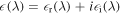 .
.  is the square of the complex refractive index. Assuming a homogeneous static electric field around the nanosphere, a collective displacement of electric charge is induced inside the material with respect to the ionic background. In alternating electric fields, that is, in optical fields, this displacement starts to oscillate, leading to a time-dependent polarization (see figure 1(a)). The sphere then acts as a nano-emitter of light.

Figure 1. Nano-optical near-fields at nanostructures. (a) Illustration of a near-field at a metallic nanosphere induced by a laser field (red). (b) Normalized local electric field strength at a gold nanosphere, λ = 720 nm.
Download figure:
Standard image High-resolution imageFor a quantitative description of the near-field, it is instructive to neglect its time dependence and weak magnetic field components and make use of the quasi-static approximation (Jackson 1999, Maier 2007). Figure 1(b) shows the calculated near-field at a gold nanosphere with a radius of 30 nm when applying an optical field with λ = 720 nm. Three main observations can be made. First, at the surface of the sphere the electric field is strongly enhanced. Second, at increasing distances from the surface into free space, the magnitude of the field rapidly decays and eventually returns to that of the externally applied field. Third, inside the sphere the local field is homogeneous and its magnitude is much smaller than that of the applied field—a screening effect. These three effects, field enhancement, field localization and screening result from charge redistribution and together form the pillar of nano-optics.
The maximum local field enhancement ξ, defined as the magnitude ratio of the total field relative to the applied field, is found at the poles of the sphere and is given by

Most significantly, ξ is independent of the radius of the sphere for spheres that are small compared to λ, but strongly dependent on the dielectric properties of the material and wavelength. The enhancement factor for the gold nanosphere at its optical 'hotspots' is ξ = 3.41 at 720 nm, corresponding to a local intensity enhancement of ξ2 = 11.6. Nonlinear processes are strongly enhanced at these hotspots, enabling low-order harmonic generation (Bouhelier et al 2003, Neacsu et al 2005a, Wolf et al 2016) and strong-field photoemission (Bormann et al 2010, Schenk et al 2010, Dombi et al 2013, Keathley et al 2013) for moderately energetic laser pulses or even continuous wave lasers (Sivis et al 2018).
Nanostructures exist in a large variety of shapes, much more complicated than spheres. Frequently used examples are nanotips, nanorods, nanotriangles and composite structures such as bow-tie antennae and dense nanoarrays. Classical electrodynamics according to the linear Maxwell equations is, in most cases, sufficient to understand and simulate the nano-optical response of such structures. Generally, near-field formation critically depends on the polarization and wavelength of the incident light, the geometry of the nanostructure and on the (wavelength-dependent) dielectric constant of the material (λ). The magnitude of the field enhancement is related to the absolute value of the complex dielectric function: the larger  , the larger ξ becomes.
The appearance of nano-optical hotspots is due to the geometry defining the boundary conditions to Maxwell's equations. The external light field induces charges at discontinuities at material interfaces and boundaries. If the polarization of the external field is aligned with the normal direction of sharp features, these charges give rise to strong local fields. The smaller the length scale of those sharp features such as their local radius of curvature with respect to the incident wavelength, the larger the field enhancement becomes. This mechanism is the time-dependent analog of the electrostatic lightning-rod effect and is a common feature for all materials.
A second geometric effect is strongly related to the wavelength of the light. A linear extension of an odd multiple of half of the wavelength can cause field enhancement significantly surpassing the other mechanisms creating an antenna resonance.
Nano-plasmonics adds a third mechanism to near-field formation, namely localized surface plasmons (LSPs). Referring to the simple example of the nanosphere, equation (1) predicts a resonance at r = −2, a condition called Fröhlich condition (Bohren and Huffman 1998). The Fröhlich condition is met by plasmonic metals in the visible spectral region (r < 0 and  ), such as gold and silver. LSPs can be excited by direct irradiation or by coupling light through a grating imprinted on the nanostructure (see, e.g. Ropers et al 2007b, Berweger et al 2012). Applying the latter method to a plasmonic nanotip leads to a traveling surface plasmon, which is focused and ultimately localized at the tip's apex (Stockman 2004). With the light on resonance, this naturally leads to higher field enhancement than other mechanisms operating in non-plasmonic materials. However, as for every resonance phenomenon, the build-up of the resonance requires a characteristic time, which may limit the suitability of such resonant structures for ultrafast processes.
2.2. Near-fields at nanotips
Nanotips are tapered needles that end in an approximately conical apex. Usually they are modeled as a hemispherical apex with radius of curvature R attached to a tapered shank with half-opening angle θ (see figure 2(a) for an illustration). The presence of the tip shank introduces a dependence of the field enhancement on both the tip radius and opening angle. Unlike for nanospheres (see equation (1)) and ellipsoids there are no analytical formulae available for the field enhancement at the nanotip geometry. The nanostructure closest to a nanotip for an analytical solution within the quasi-static approximation is an ellipsoid (Novotny and Hecht 2012). One therefore relies on numerical methods to solve Maxwell's equations for a realistic incident light field incorporating the nanotip's geometrical boundary conditions. Widely used numerical methods in nano-optics are the finite element method, the finite-difference time-domain (FDTD) method or the boundary element method (BEM) (Taflove and Hagness 2005). In the context of strong-field photoemission, both FDTD and BEM have been successfully applied (see, for example, the works of Yanagisawa et al (2009, 2010), Thomas et al (2013, 2015), Förg et al (2016), Ahn et al (2016, 2017) for FDTD and the study of (Thomas et al 2015) for BEM). In addition, a discontinuous Galerkin time-domain method has been developed for nanotips (Swanwick et al 2014). Finite element methods have been used for simulating static fields around a nanotip once it is integrated into an electron optical device (see, e.g. Paarmann et al 2012, Hoffrogge et al 2014, Bormann et al 2015 McNeur et al 2016, Storeck et al 2017).

Figure 2. Near-fields at nanotips. (a) An FDTD calculation solving Maxwell's equations yields the local electric field strength at the time when the near-field induced by a 5 fs, 800 nm laser pulse is at its maximum. The nanotip is characterized by the tip radius R and the (half-)opening angle α (here R = 10 nm and θ = 15°). The laser field E is linearly polarized along the tip's pointing direction and travels in the y direction. Gray arrows indicate the local field direction. (b) Dielectric function for various materials. Real parts r and imaginary parts i of the complex dielectric function for tungsten (W), aluminum (Al), gold (Au) and silicon (Si) as functions of wavelength λ (color). (c) Maximum field enhancement ξ for tungsten and gold nanotips with varying radius and opening angle (τ = 5 fs, λ = 800 nm). Adapted from Thomas et al (2015). © IOP Publishing Ltd. CC BY 3.0.
Download figure:
Standard image High-resolution imageFigure 2(a) shows the calculated field strength as a function of position for a tungsten tip with R = 10 nm and θ = 15° and an incident laser pulse with a full width at half maximum (FWHM) intensity duration of τ = 5 fs and central wavelength λ = 800 nm (Thomas et al 2015). The field is polarized parallel to the tip axis. In this configuration, the main features of near-field optics, namely field enhancement, localization and screening of the incident optical field become apparent. The tip is acting as a highly effective antenna for the optical field and exhibits strong-field enhancement, with ξ ∼ 6.5, close to the apex of the tip. Away from the tip surface, along the symmetry axis, the near-field strongly decays near-exponentially and relaxes to the field strength of the incident field. The decay length lF is typically of the order lF ∼ 0.8 ... 0.9R and scales approximately linearly with R. The value of lF is crucial when describing sub-optical-cycle electron acceleration driven by the near-field (see Chapter 7). Inside the tip, screening results in a highly reduced field.
Nanotips for strong-field photoemission can be fabricated from various conductive materials, such as tungsten, gold, silver, aluminum or doped silicon (see Chapter 3 for methods of tip fabrication and characterization). As discussed above, it is desirable to either choose a dielectric material with a large absolute value of the dielectric function (λ) or to employ an LSP resonance in a plasmonic material. Figure 2(b) displays the wavelength-dependent dielectric function of various materials. For tungsten, gold and aluminum, moving to longer wavelength in the near-infrared or mid-infrared domain will increase  and hence the field enhancement. The increase is most pronounced for aluminum. Already at 800 nm, the dielectric function is = −64 + 47i. In addition, gold provides plasmonic near-field enhancement because its dielectric trajectory in the complex plane (figure 2) passes near r = −2, the Fröhlich resonance condition for nanospheres (equation (1)). Note that doped semiconductors such as silicon can also exhibit strong-field enhancement.
Figure 2(c) shows the geometry dependence of the maximum field enhancement as a function of R and θ for tungsten and gold tips irradiated by a typical ultrashort laser pulse of 5 fs duration and λ = 800 nm (Thomas et al 2015). Three main observations can be made from the numerical FDTD calculation. First, ξ decreases monotonically with increasing R for both materials and for any given θ, as expected. The dependence on R is confirmed by measurements performed on tungsten and gold tips (Thomas et al 2013, Krüger et al 2014; see figure 3). Second, θ has a strong influence on the field enhancement, with maxima around θ = 40° and θ = 15° for tungsten and gold, respectively. The non-monotonic dependence on θ and the appearance of a maximum at intermediate θ for both dielectric and plasmonic materials can be traced to the build-up of the surface charge density. Its magnitude is controlled by the interplay between the illuminated surface area increasing with θ and the normal component of the electric field decreasing with θ, as predicted by electrostatics. For plasmonic materials, this effect is further enhanced by the excitation of a surface plasmon, where the resonance condition linking the dielectric constant, wavelength and opening angle leads to a maximum at smaller angles. This enhancement favors the fabrication of tips with small radii and with opening angles near the maximum. Third, the maximum enhancement in the calculated parameter space is ξ = 36 at θ = 15° for gold, much larger than for tungsten with ξ = 12 at θ = 35° due to the plasmonic response.

Figure 3. Measured field enhancement factors at tungsten and gold nanotips. Field enhancement factor of tungsten tips (blue dots) and gold tips (red squares) as a function of the tip radius. Uncertainty in ξ represents an estimated systematic error due to the uncertainty in laser intensity. Lines show the results of a numerical calculation of Maxwell's equations for 800 nm 5.5 fs laser pulses (W: solid blue line, Au: dashed red line). Reproduced from Krüger et al (2014). © IOP Publishing Ltd. All rights reserved.
Download figure:
Standard image High-resolution imageThe collective electronic response of the medium leads to a phase shift Δϕ between the incident field and the resulting optical near-field. The magnitude of this retardation effect also depends on the nanotip geometry and material, but not as strongly as ξ. For the parameters used in figure 2(c), the simulations show that tungsten and gold exhibit shifts of Δϕ ∼ 0.3 ... 0.6π and Δϕ ∼ 0.4 ... 0.7π, respectively. Under pulsed irradiation, the optical response of the nanotip also leads to small changes in the central wavelength and pulse duration. In the case of a plasmonic response, long-lived plasmon oscillations might persist after excitation (see, e.g. Sönnichsen et al 2002). Nonlinear effects such as second harmonic generation (Bouhelier et al 2003) can also influence the optical near-field.
Measuring the strength and shape of near-fields at nanotips and other nanostructures is possible using a variety of methods. Nonlinear processes driven by the near-field such as second harmonic generation (Bouhelier et al 2003, Neacsu et al 2005a), two-photon photoemission (Tsujino et al 2009), multiphoton photoemission and strong-field photoemission (Hommelhoff et al 2006b, Ropers et al 2007c, Grubisic et al 2013, Park et al 2013, Thomas et al 2013, Krüger et al 2014, Rácz et al 2017) are extremely sensitive to the enhancement. Some of the latter investigations also exploit electron acceleration or recollision driven by the near-field in order to retrieve the local intensity (for more details, see Chapter 10). Other methods rely on the interaction of a tightly focused high-energy electron beam passing by the nanostructure. The near-field manifests itself in triggering cathodoluminescence (Vesseur et al 2007, Chaturvedi et al 2009), incoherent energy loss of the electron beam (Nelayah et al 2007, Huth et al 2013, Schröder et al 2015b, Yalunin et al 2016) or coherent electron energy loss and gain (Barwick et al 2009, Feist et al 2015), enabling its spatio-temporal characterization. Attosecond nanoplasmonic streaking (Stockman et al 2007, Süßmann and Kling 2011), has been applied to measure the amplitude and phase of a near-field at a nanotip (Förg et al 2016). Recently, an experiment using terahertz streaking successfully resolved surface plasmon propagation at a nanotip (Wimmer et al 2017).
So far, we have discussed optical near-fields within the scope of classical electrodynamics, which is sufficient for most applications. However, quantum effects can become important when considering nanostructures, opening up 'quantum plasmonics' (see Zhu et al (2016) for a recent review). For example, material-vacuum boundaries should not be considered to be infinitely thin. Instead, the electron density at the surfaces is smeared out and slightly leaks into the vacuum (Zuloaga et al 2010). This can lead to an effective decrease of the magnitude of field enhancement (Zuloaga et al 2010, Ciracì et al 2012) and can affect plasmonic antenna resonances in the nano-gap between two nanostructures (Marinica et al 2012, Savage et al 2012, Scholl et al 2013, Marinica et al 2015). Ab initio theory approaches, such as time-dependent density functional theory (TDDFT), are able to provide a self-consistent treatment including such quantum effects, but suffer from technical limits of current computing power. An alternative approach introduces quantum modifications to Maxwell's equations (Esteban et al 2012, 2015). To the best of our knowledge, these effects have not been observed for strong-field-driven nanostructures. The measurement shown in figure 3 is consistent with the description by Maxwell's equations.
Experiments towards and in the strong-field regime were carried out mostly with nanotips, but there are related experiments with other types of nanostructures, such as free-standing nanowire tips with sharp edges (Ahn et al 2017), nanospheres (Schertz et al 2012), nanorods (Sun et al 2013, Kusa et al 2015, Lehr et al 2017), nanotriangles (Putnam et al 2017), nanostars (Sivis et al 2018), carbon nanotubes (CNTs) (Li et al 2017), composite bow-tie antennas and nanorod antennas (Dombi et al 2013, Rybka et al 2016, Hobbs et al 2017, Putnam et al 2017, Rácz et al 2017). In most of these experiments, the nanostructures were located on substrates and were made from gold, hence enabling plasmonic field enhancement when on resonance. In addition, gas-like ensembles of dielectric nanospheres (Zherebtsov et al 2011, Süßmann et al 2015, Seiffert et al 2017a, 2017b), metallic nanoclusters (Passig et al 2017) and C60 'buckyballs' (Li et al 2015) were used in strong-field experiments.
3. Experimental methods
In this chapter, we briefly introduce the experimental methods that enable strong-field studies at nanotips and other nanostructures. Figure 4 shows a typical experimental setup. Femtosecond laser pulses are focused onto the apex of a metallic nanotip situated in an ultrahigh vacuum chamber. Pressures ideally below 10−8 Pa are helpful to maintain atomically clean surfaces over at least one hour. The laser polarization axis is parallel to the tip's symmetry axis, enabling maximum field enhancement and pronounced photoemission in the forward direction. Photoelectrons are usually detected using either a detector with spatial resolution to image the emission pattern or an electron spectrometer to measure the photoelectron spectrum. In the following, we will focus on each element in more detail.

Figure 4. Typical experimental setup for strong-field photoemission from a metal nanotip. A linearly polarized beam consisting of femtosecond laser pulses (red) is focused on the apex of a metallic nanotip with the help of an off-axis parabolic mirror (OAP). Electrons (blue) are emitted in forward direction and are detected either using a micro-channel plate (MCP) detector for spatial resolution or an electron spectrometer for spectral resolution. The transmitted laser beam can be used for diagnostics.
Download figure:
Standard image High-resolution imageInitial experiments used widely available titanium sapphire-based laser sources at a center wavelength around 800 nm generated by both high repetition rate laser oscillator and low-repetition rate amplifier systems. In oscillator-based experiments, the damage threshold of the tungsten nanotip prevented the use of enhanced peak intensities Ieff of more than  (Krüger et al 2011). Using kHz repetition rate systems, higher intensities could be reached, for instance
  for 30 fs, 800 nm pulses (Bormann et al 2010) and a similar value for 4 fs, 700 nm pulses (Hoff et al 2017b). Working towards applications of laser-triggered nanotips as coherent electron guns, blue or UV laser pulses were employed (see, for example, Ehberger et al 2015, Bormann et al 2015, Storeck et al 2017). On the high-frequency frontier, single isolated attosecond XUV pulses were applied in order to perform attosecond nanoplasmonic streaking (Förg et al 2016). In the mid-infrared spectral region, experimental studies relied on fiber lasers (see, e.g. Thomas et al 2012, Rybka et al 2016, Putnam et al 2017) or tunable systems based on optical parametric amplification (see, e.g. Herink et al 2012, Park et al 2012, Homann et al 2012, Piglosiewicz et al 2014, Förster et al 2016, Schötz et al 2018). Also, THz pulses were added to the repertoire of light sources, effectively providing a quasi DC electric field transient strongly localized at the nanotip (Herink et al 2014, Wimmer et al 2014, Li and Jones 2016, Wimmer et al 2017). The laser pulses were delivered onto the sample most often with reflective optics, such as off-axis parabolic mirrors or Schwarzschild-type microscope objectives to prevent chromatic aberration and dispersion effects. Overlapping the nanotip apex with the laser focal spot can be achieved with the help of 3D nanopositioning translation stages.
Most experiments are carried out in ultrahigh vacuum, helping to avoid surface contamination of the sample and allowing the operation of electron multipliers. An exception are nano-devices in ambient air where the gap between the sample and detection electrode is less than 5 μm, sufficient for electron diffusion to the detector (Rybka et al 2016, Putnam et al 2017). Nanotips from some materials can be produced from monocrystalline and polycrystalline wires by electrochemical etching, for example, tungsten tips (Klein and Schwitzgebel 1997) and gold tips (Neacsu et al 2005b, Eisele et al 2011). Tungsten and to a lesser degree gold enable the use of field emission microscopy (Fursey 2005) and field ion microscopy (Müller 1965, Panitz 1982) in order to characterize the field emission properties and the atomic-scale crystallographic surface structure of the tip apex. Field evaporation (Tsong 1990) and resistive flash heating are two techniques to clean the tip in situ. State-of-the-art nanofabrication techniques such as electron-beam lithography, focused ion beam milling and epitaxial deposition significantly extend the range of materials and geometries. For example, recent investigations employed molybdenum nanotip arrays (Mustonen et al 2011), gold nanorod arrays (Dombi et al 2013), pillar arrays (Nagel et al 2013) and junction devices (Rybka et al 2016), silver tips (Bionta et al 2016), doped silicon tip arrays (Swanwick et al 2014), hafnium carbide nanotips (Kealhofer et al 2012) and carbon cone nanotips (Bionta et al 2014). In addition, carbon nanotube (CNT) arrays were used for strong-field experiments (Li et al 2017).
Detection is typically focused either on spatial resolution or spectral resolution. Spatial information can be gained in a field emission microscope setup where the nanotip is combined with an MCP detector with a phosphorus screen, located a few cm away from the tip (see figure 4 and Yanagisawa et al (2009) for example experimental setups). The spatial emission pattern of field emission or photoemission is mapped on the MCP with a spatial magnification of up to 106, enabling nanometric resolution without additional electron optics. Chevron-type MCPs allow detecting emitted electrons with a typical efficiency of roughly 50%. Spectral resolution is achieved by electron spectrometers either based on time-of-flight measurements of laser-triggered electrons (Hilbert et al 2007, 2009, Keathley et al 2013, Hoff et al 2017b) or on electrostatic techniques. Typically, retarding field (see, e.g. Schenk et al 2010, Herink et al 2012) or hemispherical analyzers (Yanagisawa et al 2011, Park et al 2012, 2013, Piglosiewicz et al 2014, Yanagisawa et al 2016) are used. Hemispherical electron analyzers have an additional advantage as they also provide angular resolution. In combination with an imaging screen around their entrance aperture, they furthermore allow for site-selective spectral measurements. Recently, a nanotip has been combined with a velocity map imaging spectrometer (Bainbridge and Bryan 2014). In order to use nanotips for electron source applications, they can be integrated into electron optical imaging systems, both on a macroscopic (Hoffrogge et al 2014) and microscopic scale (Lüneburg et al 2013, Bormann et al 2015, Storeck et al 2017). Typically, a negative bias voltage VDC is applied between nanotip and detector, leading to a static electric field of magnitude 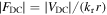 at the tip's apex. The geometry-dependent field reduction factor kr ranges, typically, from 5 to 15 for nanotips.
4. Photoemission mechanisms
The near-field induced at nanotips and other nanostructures opens the door to strong-field photoemission with field strengths in excess of 1 V Å−1. This is the central theme of this article, as it enables strong-field physics. In analogy to gas-phase atomic photoionization, photoemission from metallic surfaces obeys the intensity-frequency scaling of Keldysh's theory (Bunkin and Fedorov 1965, Keldysh 1965). The dimensionless Keldysh parameter γ is given by

where the work function W for the least bound electrons in the solid replaces the binding energy of the electron in the atom. The ponderomotive energy Up

describes the mean quiver energy of a free electron (electron mass m and charge e) in a monochromatic light field of amplitude F0 and angular frequency ω. For the case of a nanotip, the field strength F0 is replaced by the corresponding near-field enhanced strength at the tip apex, Feff = ξ · F0. The Keldysh parameter separates two limiting photoemission regimes, the multiphoton regime (γ ≫ 1) and tunneling regime (γ ≪ 1). In the multiphoton regime, the action of the light field on the electrons at a metal surface can be treated within a perturbative approach. In the tunneling regime, this approach inevitably breaks down since the laser field strength is starting to compete with the strength of the field binding the electrons within the metal. In the following, we will survey important photoemission mechanisms occurring at metal nanotips and discuss their signatures in experimental data.
4.1. Photoemission assisted by a strong static electric field
In contrast to extended flat metal surfaces (and to nanoparticles in the gas phase), metal nanotips offer the possibility of also applying a static electric field sufficiently strong for field emission. At the tip apex, local field strengths of up to −2 GV m−1 can be easily attained and provide an additional control knob not available in other geometries. The static field can also be made slowly time-dependent by applying voltage pulses (nanosecond time scale, Ganter et al (2008)) or THz fields (picosecond to femtosecond time scale, see, e.g. Wimmer et al (2014), Herink et al (2014), Li and Jones (2016), Wimmer et al (2017)). Before discussing multiphoton and tunneling photoemission, we will sketch three emission mechanisms that are enabled by the static field: photoemission assisted by the Schottky effect, photofield emission and thermally enhanced field emission.
4.1.1. Photoemission assisted by the Schottky effect
The photoelectric effect is conceptionally the simplest and most fundamental photoemission mechanism. Accordingly, the energy carried by a single photon must be larger than the work function of the metal, requiring light in the deep UV spectral region for most materials (Einstein 1905). At metal nanotips, applying a static electric field leads to a significant reduction of the potential barrier (see figure 5(a)). This effect is known as the Schottky effect, here occurring at the metal-vacuum interface (Schottky 1914). The effective decrease ΔWs of the work function is given by

Figure 5. Emission mechanisms assisted by a static field. (a) Photoemission assisted by the Schottky effect. The work function is lowered by ΔWs due to the Schottky effect, enabling photoemission at photon energies below W. (b) Photofield emission. After gaining the energy of a photon, an electron is emitted by field emission. (c) Thermally enhanced field emission. The laser pulse is heating the conduction-band electrons, resulting in field emission of excited electrons.
Download figure:
Standard image High-resolution imageThe Schottky effect enables single-photon (and two-photon) photoemission at photon energies well below the work function as ΔWs can reach up to −2 eV. Laser-triggered electron gun designs employ this mechanism to localize the emission to the tip apex (see section 10.2). The static field can even be used to shape the energy distribution of the emitted electron pulses by tuning the work function in order to minimize chromatic electron propagation effects (Hoffrogge et al 2014, Ehberger et al 2015).
4.1.2. Photofield emission
Photofield emission, also called photo-assisted field emission, consists of two steps (Lee 1973, Radoń 1998). First, electrons are excited by single-photon absorption to unoccupied conduction band states. Second, field emission induced by the static field leads to emission of these electrons from the metal surface (see figure 5(b)). The photofield emission rate depends both linearly on laser intensity and nonlinearly on the static field strength at the surface described by the Fowler–Nordheim (FN) theory (equation (5)). The work function W has then to be replaced by a reduced barrier height W − ℏω (Lee 1973, Hommelhoff et al 2006c). The resulting photoelectron spectrum is a convolution of the laser spectrum with the projected surface density of states along the laser polarization axis and with the tunneling probability from the field emission step (Rethfeld et al 2002). Photofield emission is particularly sensitive to electronic decoherence effects in the metal. Electron–electron and electron–phonon scattering inherent to metals and space-charge effects can strongly influence the electron momentum spectrum on time scales larger than 10 fs (Rethfeld et al 2002, Yanagisawa et al 2011, Wendelen et al 2013, Yanagisawa et al 2016). Photofield emission is not restricted to single-photon absorption; recently, also two-photon absorption and subsequent field emission was found at tungsten tips (Yanagisawa et al 2011, Yanagisawa 2013).
4.1.3. Thermally enhanced field emission
Thermally enhanced field emission is also a two-step process (Lee 1973, Kealhofer et al 2012) (see figure 5(c)). Compared to photofield emission, the first step is of a slightly different nature. Laser light strongly excites electrons within the metal, creating a non-equilibrium electron distribution. For a thermalized system of conduction-band electrons, this corresponds to heating to temperatures of the order of 1,000 K (Lisowski et al 2004). During and after heating of the electron gas, electrons transiently occupy states above the Fermi level. These electrons can undergo field emission if a strong static electric field is applied to the tip. On the time scales of several hundred femtoseconds to picoseconds after the excitation, electron–phonon scattering sets in, leading to a full thermalization of the metal (Vurpillot et al 2006, Gault et al 2007). The heating effect depends on many quantities such as laser average power and peak intensity, pulse duration and material properties, and competes with all other emission mechanisms. According to the detailed investigation by Kealhofer et al (2012), the (electronic) thermal conductivity is of particular importance. For instance, hafnium carbide, despite its high melting point and due to its poor electronic thermal conductivity is much more prone to thermal effects than metals such as gold and tungsten. Thermally enhanced field emission has been found to be highly nonlinear in the laser intensity, more than the usual multiphoton scaling, and exhibits a strongly localized emission pattern resembling field emission (Kealhofer et al 2012).
4.2. Multiphoton and above-threshold photoemission
In close analogy to multiphoton ionization in the gas phase, solid surfaces enable multiphoton photoemission (MPP). Its main experimental signature is the power-law scaling of the emission rate w with intensity I0,  , where nmin is the minimum number of photons required to overcome the work function. MPP is associated with Keldysh parameters γ ≫ 1. Many experimental studies at metal nanotips demonstrated MPP, for instance Ropers et al (2007a, 2007c), Barwick et al (2008), Tsujino et al (2008), Hilbert et al (2009) and Yanagisawa et al (2011). Only recently, an experiment identified three-photon MPP by a continuous wave laser field, exploiting the strong near-field enhancement at metallic nanostar structures (Sivis et al 2018). MPP is usually mediated by virtual intermediate states or by resonant states. Resonances allow for coherent control scenarios, where the spectral amplitude and phase of a light field controls the spectral amplitude and phase of an electron wavepacket (see section 10.1).
Moving towards higher intensity and lower γ, substantial contributions from higher multiphoton orders n > nmin are expected. More photons than are required to free an electron are absorbed and ATP takes place, first observed at flat metallic surfaces (see Luan et al 1989). Detecting ATP requires spectrally resolved photoelectron measurements because the photocurrent-intensity power law will be dominated by the lowest multiphoton order. Figure 6(a) displays the first observation of ATP at a nanotip, recorded at different incident light intensities (W, λ = 800 nm) (Schenk et al 2010). With increasing intensity more ATP peaks appear, corresponding to the number of absorbed photons. The spectrum decays exponentially with increasing kinetic energy, as expected from theory (see Chapter 5). The dependence of the total photocurrent on intensity shows that three-photon MPP dominates for all intensities, overshadowing the higher orders appearing in the spectral measurements (figure 6(b)). ATP at nanotips and other nanostructures has been measured with spectral resolution in many systems and wavelength regimes, many of them in the strong-field and tunneling regimes. Prominent examples are Herink et al (2012) (Au tip, 800 nm to 8 μm), Park et al (2012) (Au tip, 1.5 μm), Dombi et al (2013) (Au nano-array, 800 nm), Swanwick et al (2014) (n-doped Si tip array, 800 nm), Bionta et al (2014) (W tip, 800 nm), Bionta et al (2016) (Ag tip, 400 and 800 nm), Förster et al (2016) (W tip, 1.55 μm) and Li et al (2017) (CNT array, 820 nm). Most of these experiments, however, do not resolve the ATP peaks; possible reasons include limited spectral resolution, space-charge broadening and thermal contributions to the emission, surface impurity of the employed emitters, a broad distribution of initial states in energy in the material or intensity averaging due to pulse envelope effects in the strong-field regime. If photon orders are not resolved, care must be taken to distinguish the prompt and coherent ATP from other emission processes.
Figure 6. Strong-field above-threshold photoemission. (a) Count rate as a function of energy for different incident peak intensities (W tip, 800 nm). From bottom to top, the intensities are  . Color symbols mark the features analyzed in (c). Inset: illustration of ATP from a metal surface. (b) Dependence of the total emission current on intensity in a double-logarithmic plot. The red line is an MPP power-law fit to the data, revealing an effective nonlinearity of n ≈ 3.1 (three-photon process). (c) Positions of n = 4 and n = 5 peaks (squares and diamonds) and two neighboring minima (circles and triangles) as function of intensity. The slopes of the linear fit curves are in the range of −1.2 to
  . Adapted figure with permission from Schenk et al (2010), Copyright (2010) by the American Physical Society.
Download figure:
Standard image High-resolution image4.3. Onset of strong-field effects
At even higher intensities and lower Keldysh parameters, the simple picture of MPP and ATP breaks down. Continuum effects gain importance, in particular the dynamics of the liberated photoelectron in the laser field, leading to shifts of ATP peaks and channel closings. The energy of each ATP multiphoton order reads: 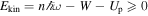 . In analogy to atomic systems (Bucksbaum et al 1987), the peaks shift towards lower energies and more and more photon orders will disappear (channel closing). A simple explanation is provided by the AC Stark effect (or light shift). During the presence of the laser pulse, the continuum states are field-dressed and upshifted in energy by the ponderomotive energy Up (Mulser et al 1993). This energy is lost after the laser pulse has ended. Strong-field effects are visible in figure 6(a). For increasing intensity, the peaks shift to lower energy and the lowest peak (n = 3) finally disappears. The shift of the spectral features is captured quantitatively in figure 6(c).
4.4. Tunneling photoemission
The occurrence of more and more channel closings leads to strong deviations from the MPP power law. The current-intensity relation turns into a tunneling rate scaling exponentially with field strength (see equation (7), Chapter 5), a hallmark of optical tunneling emission. Indications for the multiphoton-to-tunneling transition at a metal surface were observed by Tóth et al (1991) and Dombi et al (2010); the first observation at a nanostructure was reported by Bormann et al (2010) at a gold tip with a low-repetition-rate amplified Ti:sapphire laser system. Figure 7(a) shows the main result of their study: a clearly resolved 'kink' in the scaling of the photocurrent with the pulse energy. A quantitative analysis reveals a pronounced decrease of the effective nonlinearity from n ∼ 5 to n ∼ 1 (figure 7(b)); the authors argued that space-charge saturation can be ruled out since the solid angle of emission measured with an MCP detector does not increase with pulse energy. Figure 7(c) shows the result of a calculation using the strong-field approximation (SFA, see section 5.3) including field penetration into the metal, clearly reproducing the transition and elucidating its origin in the progressive closing of more and more channels.

Figure 7. Transition from the multiphoton to the optical tunneling regime. (a) Hallmark of the transition is the 'kink' in the current-intensity (pulse energy) scaling (here: Au tip, 830 nm). The slope in the double-logarithmic plot is changing rapidly from a multiphoton power-law scaling to a tunneling rate behavior (blue circles: experimental data; dashed black line: multiphoton power law; red curve: SFA calculation). Insets: single-shot images of the emission patterns. (b) Dependence of the effective nonlinearity (red squares) and solid angle of emission (green circles) on pulse energy. (c) Results of an SFA calculation including field penetration (total emission rate: solid black curve; selected individual channels: colored curves). Increasing the intensity (decreasing γ) leads to the closing of more and more channels, resulting in the 'kink'. Adapted figure with permission from Bormann et al (2010), Copyright (2010) by the American Physical Society.
Download figure:
Standard image High-resolution imageThe transition marked by the 'kink' has been observed and studied in a wide range of systems. Among them are Keathley et al (2013) and Swanwick et al (2014) (n-doped Si tip array, 800 nm), Hobbs et al (2014) (Au nano-array, 800 nm), Piglosiewicz et al (2014) (Au tip, 1.65 μm), Kusa et al (2015) (Au nano-array, 3 ... 10 μm), Rybka et al (2016) (Au nano-gap device, 1.5 μm), Putnam et al (2017) (Au nano-array device, 1 μm), Li et al (2017) (CNT, 820 nm) and Keathley et al (2017) (n-doped Si tip array, 800 nm). In some studies, including the pioneering work (Bormann et al 2010), the transition is quite sharp, unlike the predictions of the SFA. Incorporating the penetration of the laser field into the metal into the SFA, as suggested by (Bormann et al 2010), can explain this sharpening; additional processes limiting the emission rate can be depletion or space-charge effects. The observation of a saturation of the intensity dependence of the current by Piglosiewicz et al (2014) is noteworthy but remained unexplained. A recent study presented by Keathley et al (2017) reveals finer structures in the scaling curve related to single-channel closing, as predicted by the SFA (Yalunin et al 2011) (see also figure 9 in section 5.3). The authors also hint at the importance of the initial density of states distribution for the shape of the transition. Recently, signatures of the transition have been observed in a very different system, a bulk semiconductor nano-device (Paasch-Colberg et al 2016).
5. Theoretical methods
A more detailed understanding of the processes involved in laser-nanotip interactions requires the development of theoretical tools which are discussed in this section. Due to the design of typical experimental setups (Chapter 3) one is confronted with a true multi-scale problem: the ground-state electronic wavefunction typically extends over distances a of one to a few Ångstroms, the quiver amplitude α of the liberated electron in the enhanced near-field may reach several nm. The tip radius is about R ∼ 10 nm and the laser wavelength λ is of the order of 1 μm. Associated time scales range from  as for the electrons in motion (vF ... Fermi velocity) over the laser period Topt ∼ 2.7 fs at a wavelength of λ = 800 nm to the duration of the laser pulse τ ≳ 5 fs.
Considering this range of length and time scales, modeling the interaction of laser pulses with metallic nanotips appears to be a formidable task. However, these widely disparate scales allow for a separation of the problem into a mesoscopic part for the propagation of the laser pulse in the presence of the metal tip (solution of Maxwell's equations; see above) and a microscopic part for the simulation of the interaction of the local electric light field with the electronic system. This is because of the negligible effect of the laser-induced electron currents (∼1 electron per pulse) on the propagation of the laser pulse. The solution of Maxwell's equations can therefore be directly used as independent input to any microscopic model for the photoelectron emission.
In the following, we will briefly review the most frequently used methods, which are capable of accounting for recent experimental observations at least on a qualitative and often even on a quantitative level. The level of sophistication ranges from semi-classical approaches including the classical trajectory Monte Carlo (CTMC) method to solutions of the time-dependent Schrödinger equation (TDSE) on a single-particle level to TDDFT as many-body description on a mean-field level. Representative examples of results from different methods and comparison with experimental data will be presented in later chapters. In this chapter, all equations are given in atomic (Hartree) units (a.u.).
5.1. (Semi-) classical trajectory simulations
In the context of laser-nanotip interactions, (semi-) classical trajectory calculations closely mirror those employed in laser-atom interactions, the most prominent of which is the well known three-step model of high-harmonic generation in laser-atom interactions. Accordingly, electrons tunnel through the barrier of the combined surface and laser potentials around the time of the maxima of the electric field (step 1). The liberated electrons are then accelerated in free space and undergo a quiver motion. Depending on the phase of the driving field at the moment of appearance at the tunneling exit and the initial momentum, electrons will be either directly emitted or are driven back towards the surface after an excursion of about the quiver radius α (step 2). A fraction of the latter electrons is eventually (back-) scattered at surface atoms and may reach the detector after a second acceleration cycle in the light field, leading to higher asymptotic kinetic energies (step 3).
The tunneling step 1 is the key non-classical ingredient which renders the three-step model semi-classical rather than classical. Its description can be traced back to the FN theory for field emission in strong static electric fields (Fowler and Nordheim 1928, Nordheim 1928). In this seminal work, the surface potential of the solid was approximated by a potential step function (deviations of the surface potential from the step function were considered negligible) of height EF + W, with EF the Fermi energy of the electron gas and W the work function of the material. Superimposed with the potential of the electric field along the surface normal, VDC = FDCz, the field-dependent current jFN was found to be proportional to

which can be directly converted into a field-dependent emission rate. A more sophisticated version of the equation also accounts for the presence of the image-force potential (see, e.g. Forbes 2006). Applicability of this simple estimate to time-dependent laser fields is far from obvious and is well justified only in the adiabatic limit. For short tunnel distances and sufficiently slowly varying fields, the static approximation provides a good estimate for, now time-dependent, tunneling rates. Keldysh succeeded in quantifying 'short' and 'sufficiently slowly' by introducing the parameter named after him (see equation (2)), which can be alternatively expressed as

relating two time scales, namely the classical time it takes an electron with velocity  to pass through a tunnel of width
  with the characteristic time of the oscillating field, i.e. the optical period Topt. For γ ≪ 1 the barrier may be assumed to be static and equation (5) or a variant thereof can be used. Typically, this condition is not fulfilled in laser-nanotip experiments. The use of equation (5) can therefore only be justified a posteriori when comparing with experimental data. For example, data from recent experimental studies of photoemission by two-color laser pulses strongly deviates from predictions based on tunneling rates. Therefore, alternative emission processes must be involved (Förster et al 2016). For atomic gases, a closed-form tunneling rate taking the time variation of the external field into account has been proposed for nonadiabatic tunneling (Yudin and Ivanov 2001). An analogous analysis for emission from metal surfaces is still missing. In most simulations, equation (5) or static emission rates derived for atoms, e.g. the Perelomov–Popov–Terent'ev (Perelomov et al 1966), Ammosov–Delone–Krainov (Ammosov et al 1986) or Delone–Krainov (Delone and Krainov 1994) rates are used. For laser fields linearly polarized in the direction of the tip axis and for an electron in the Fermi gas with a binding energy in the range of
  , application of equation (5) for a 'slowly' varying laser field gives rise to a time-dependent emission rate
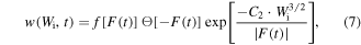
where ![$f[F(t)]$](https://content.cld.iop.org/journals/0953-4075/51/17/172001/revision2/jpbaac6acieqn16.gif) is a field-dependent prefactor to the dominant exponential and C2 a constant. The Heaviside Θ-function ensures that, unlike for atoms, emission takes place only during laser half-cycles with negative field, i.e. when the barrier is lowered toward the vacuum side. It is important to note that in this context
is a field-dependent prefactor to the dominant exponential and C2 a constant. The Heaviside Θ-function ensures that, unlike for atoms, emission takes place only during laser half-cycles with negative field, i.e. when the barrier is lowered toward the vacuum side. It is important to note that in this context  is the kinetic energy of a free electron in the direction of the surface normal. In simple estimates only electrons from the Fermi edge with Wi = W are considered. For an improved simulation, emission rates
  are weighted with the projected density of states
  or, more accurately, the projected surface density of states (SDOS). The simplest and most popular choice is the SDOS of a free-electron gas,
 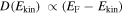 .
.
The tunneling process not only governs the emission rate equation (7) but also the momentum and spatial distributions, i.e. the phase-space distribution of the liberated electron. This distribution provides the initial conditions of the subsequent classical trajectory calculation. A wide variety of choices of initial conditions are available.
As for tunneling emission from atoms, position and momentum distributions at the tunnel exit are a matter of debate and cannot be reconstructed unambiguously. Estimates for parallel and perpendicular momentum distributions are available for atoms (e.g. Delone and Krainov 1994, Popov 1999), but are missing for metal surfaces. Often, the simple ansatz for the position at the geometric tunnel exit,  and p0 = 0 is used (Krüger et al 2011, 2012a). More sophisticated approaches include corrections of the position z0 due to the presence of the image potential,
  , and using a Gaussian momentum distribution for the emitted electron, thereby approximately accounting for the position-momentum quantum uncertainty.
In step 2, the electron trajectory can now be easily simulated numerically by solving Newton's equation of motion for a charged particle in the combined fields of the surface and the external laser pulse,

where p is the momentum along the surface normal and F(z, t) is the effective near-field discussed in Chapter 2.
Depending on the time of emission and their initial momentum, electrons may escape from the tip region and reach the detector directly or they may be driven back to the surface of the solid (indicated in figure 8 by the small light blue wavepackets). In the former case, a Gaussian momentum distribution at the tunnel exit will directly result in an exponentially decreasing low-energy spectrum reaching up to about  (Milošević et al 2006) with a width (1/e-intensity) directly related to the width of the momentum distribution at the tunnel exit. Comparison between experimental and simulated energy spectra in the low-energy region therefore gives information on the momentum distribution of photoelectrons upon release from the surface.
Figure 8. Electron dynamics after tunneling. (a) Orange line: laser electric force, blue: direct wavepackets, light blue: rescattered wavepackets, dashed lines: trajectories suppressed due to screening of the electric field at the surface of the tip. (b) Exponentially decreasing spectrum due the first direct wavepacket  (blue filled curves). (c) The plateau forms due to rescattering of the wavepacket
  (green filled curves). (d) Repetition of the electron emission after one optical cycle Topt = 2π/ω gives rise to interference fringes in the energy spectra between wavepackets
  and
and  . (e) The full spectrum also includes interferences between rescattered wavepackets
  and
and  and closely resembles the experimental spectrum (pink). Reproduced from Krüger et al (2012b). © IOP Publishing Ltd and Deutsche Physikalische Gesellschaft.CC BY-NC-SA 3.0.
Download figure:
Standard image High-resolution imageFor a moderate intensity of the IR laser field of  at λ = 800 nm well below the damage threshold, the quiver amplitude in the enhanced near-field,
  a.u. is still small compared to the characteristic distance over which the near-field enhancement decays. Therefore, one can simulate the trajectories in a spatially homogeneous enhanced field ξ · F(t).
An electron emitted at the maximum of the field is accelerated first towards vacuum for a quarter of an optical cycle. When the direction of the field reverses it is decelerated and finally driven back towards the surface which it reaches close to the end of the next half-cycle with a kinetic energy of up to 3.17 Up (Milošević et al 2006).
While this is the maximum energy for recombination and, hence, high-harmonic generation, for electron emission the third step involves elastic scattering at the surface. For scattering angles close to Δθ ≈ π the momentum direction is impulsively reversed, allowing now for an additional acceleration in the complete subsequent half-cycle and leading to final energies of up to 10.007 Up (second classical cut-off).
The time evolution of the wavefunction of a free electron in momentum space from emission time t0 to rescattering time ts is given by Volkov (1935) as

where the Volkov phase is given by the classical action integral,

In a semi-classical approximation for the free-particle propagation, the classical trajectories are endowed with phases given by the classical actions. Consequently, the Volkov phase  (equation (10)) enters also the semi-classical description of strong-field dynamics, which allows to selectively incorporate quantum effects (Krüger et al 2011, 2012b). This can be viewed as a partial sum over those paths contributing to the Feynman path integral that do not involve classically forbidden trajectories.
The quantitative importance of the third step is controlled by the backscattering cross-section. For the latter, a variety of approximations are in use ranging from hard-wall scattering ( ), which is sufficient to reproduce the plateau and cut-off energy of the photoelectron spectrum (Krüger et al 2011), to full quantum mechanical doubly differential elastic scattering probabilities (cross-sections) for surface atoms modeled by muffin-tin potentials, which also allow to reproduce the relative heights of direct peak and plateau (Salvat et al 2005, Wachter et al 2012). In the energy range considered here, the elastic scattering probability for electrons with Ekin ≲ 20 eV off heavy atoms can reach 10%–20%.
Based on the three steps discussed above, the main features of the energy spectrum of photoelectrons emitted in ultrashort laser-nanotip interactions can be reproduced: the exponential drop at low energies and the formation of a plateau with its carrier-envelope phase-dependent cut-off energy (Krüger et al 2011, Wachter et al 2012). In addition, more complex scenarios can be simulated, in particular those including the spatial decay of the nano-optical near-field in one or more dimensions. However, the notion of rescattering breaks down if the quiver length is of the order of the near-field decay length or larger (see Herink et al (2012), Park et al (2012), Yalunin et al (2013), Piglosiewicz et al (2014), Echternkamp et al (2016b); and Chapters 7 and 8).
5.2. Simple man's model for nanotips
If interference effects such as the ATP peaks and modulations in the electron spectrum are also to be included within a rescattering model, point-like classical electrons have to be replaced by quantum mechanical or semi-classical wavepackets. Here, we formulate a simple man's model for nanotips (SMMNs), accounting for quantum effects. Considering that electron emission is confined to the tip apex (R ∼ 10 nm), which is much larger than the characteristic length of the electron wavefunctions (Fermi wavelength λF ∼ 0.1 nm), we find that translational symmetry of the electron subsystem is approximately conserved in the surface plane, allowing for a quasi-1D treatment along the surface normal z.
For a monochromatic vector potential,  , integral (10) can be solved,
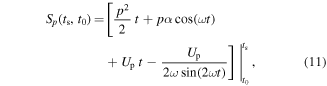
and we obtain the wavefunction emitted at time t0 as

Directly emitted electrons will therefore show a momentum spectrum of  or, equivalently, an energy spectrum exponentially decaying with decay constant
  . σp can be determined directly from comparison with experimental energy spectra or estimated from theory (Popov 1999).
Those parts of the wavepacket that return to the surface at time ts are assumed to be elastically rescattered, reversing their kinetic momentum. After conclusion of the pulse this part of the initial wavepacket will have a momentum spectrum shifted by  ,
,

Choosing t0 and ts to maximize pr gives the cut-off energy  . The sum of direct and rescattered momentum spectra can account for the overall shape of the energy spectrum quite well (Krüger et al 2012b).
Periodic repetition of emission and rescattering of wavepackets in subsequent laser cycles at times  and coherently summing up their contributions results in the emergence of the characteristic ATP peaks in the energy spectrum. Assuming only two wavepackets launched at subsequent field maxima (t0 = 0, t1 = Topt) yields the final momentum spectra for the direct and rescattered parts,
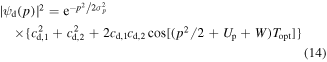
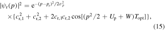
with ATP maxima at  . The large separation of the two contributions in momentum space (p0 ≪ pr ) allows for a final incoherent summation to obtain the momentum spectrum,
  , which closely resembles experimental spectra. In fact, the prediction (equations (14), (15)) is sufficiently close to the observed spectrum that it can be used to directly determine the effective field strength (the free parameter in the model) present in the experiment. To this end, the static field also present should be taken into account. It causes an effective decrease of the work function due to the Schottky effect (see equation (4)). It also leads to a slight decrease of the cut-off energy,
  (Krüger et al 2012b).
Related concepts have been discussed for electron emission from solid surfaces (Yalunin et al 2011, see next section). In this case, however, the microscopic (electronic subsystem) and macroscopic (pulse propagation) models cannot be separated due to the large extension of the surface. Intensity averaging over the beam spot and beam-propagation effects erase irreversibly most of the information about details of the photoexcitation process (Lemell et al 2003, Apolonski et al 2004), highlighting the importance of studies of photoemission from nanostructures.
5.3. Strong-field approximation
The SFA, also called Keldysh–Faisal–Reiss theory (Keldysh 1965, Perelomov et al 1966, 1967, Faisal 1973, Reiss 1980, Gribakin and Kuchiev 1997), successfully describes photoionization of atoms and negative ions triggered by strong laser fields. It corresponds to a version of a first-order distorted-wave Born approximation. The distorted waves used as the final state in the photoionization process are the Volkov wavefunctions describing free electrons driven by a light field (see equation (9)), where the atomic potential is neglected after ionization took place. The SFA to the TDSE is applicable for calculating electron spectra and ionization rates for all Keldysh parameters γ, provided that the ionization potential is much larger than the photon energy of the driving-laser field.
The SFA has been first applied to strong-field photoemission from surfaces by Bunkin and Fedorov (1965). Neglecting the projected SDOS, the strongly nonlinear dependence of the emission rate on the binding energy suggests that the dominant emission processes can be captured by studying the time evolution of a single active electron at the Fermi energy, i.e. with a binding energy equal to the work function of the material. The SFA rate as a function of final drift momentum p is given by a sum over all channels corresponding to the absorption of n photons,
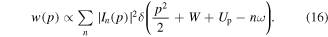
Here, we assume a reduction of the problem to one dimension and excitation by a quasi-monochromatic laser field. The theory correctly predicts ATP peaks enforced by the energy conservation law in the delta function. The peaks are shifted to lower energies by the ponderomotive energy Up. The SFA naturally describes channel closing, i.e. due to the ponderomotive action ionization channels are successively suppressed as the field strength is increased. Neglecting all spatial dependencies of the transition matrix elements, the coefficients In(p) are given by
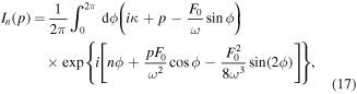
with  (see Yalunin et al 2011). The argument in the exponent is related to the action. The integral can be calculated numerically. Alternatively, the total emission rate can be obtained to a good degree of approximation using a saddle-point approach. The generalized Keldysh rate, which covers all γ with exponential accuracy (Bunkin and Fedorov 1965, Keldysh 1965, Perelomov et al 1966, Tóth et al 1991) is
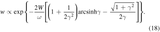
At large γ, in the multiphoton regime, the total photoemission rate scales with intensity as a power law,  , where nmin is the minimum number of photons required to overcome the binding energy. In turn, the tunneling-like behavior (see equation (7)) at higher intensities is the consequence of a rapid sequence of channel closings (see Bormann et al (2010), Yalunin et al (2011) and figure 7).
Application of the SFA to electron emission from the metal-vacuum interface requires modifications and extensions compared to the atomic case due to the broken inversion symmetry along the surface normal. The laser field is strongly screened inside the metal and only acts in the vacuum half-space. Emission only takes place into the positive half-space away from the surface. Furthermore, inclusion of the rescattering process, which provides a much stronger contribution for surfaces than for atoms because of the extended nature of the target, requires a treatment beyond first-order distorted-wave perturbation theory (Milošević et al 2006). So far, most investigations have resorted to atom-like semi-classical models, as described in the previous sections, and only consider electron trajectories on the vacuum side of the interface. Accurate total photoemission rates, however, require the inclusion of rescattering at the surface, in particular in the weak-field regime γ > 1.
In a thorough theoretical study by Yalunin et al (2011), a time-periodic Green's function approach has been applied to the problem, providing an approximate solution that includes the effect of the surface. The key idea is to consider contributions to the total ionization rate due to the reflection of waves at the surface, with the help of field-dependent reflection coefficients. This can lead to an increase of the ionization rate compared to the plain SFA and deviations from the power-law scaling in the multiphoton regime. The results of the modified SFA compare well with Floquet solutions and with a numerical integration of the TDSE (see figure 9). A different embodiment of the SFA includes the influence of field penetration into the metal, influencing the position and shape of the multiphoton-tunneling transition (Bormann et al 2010).

Figure 9. Comparison between different theoretical approaches. Photoemission rate as a function of Keldysh parameter γ or field strength (800 nm, W = 5.5 eV): perturbative SFA calculations (solid orange) are compared to a TDSE solution using the Crank–Nicholson approach (solid green) and Floquet calculations of the four-photon (dashed blue) and five-photon (dot-dashed blue) amplitudes. Adapted figure with permission from Yalunin et al (2011), Copyright (2011) by the American Physical Society.
Download figure:
Standard image High-resolution imageFor a proper description of rescattering photoelectron spectra, a second-order SFA borrowed from atomic physics should be applied (see, e.g. Milošević et al (2006) for the atomic case). Most importantly, the theory predicts interferences of short and long trajectories, photoelectron yield beyond the classical rescattering cut-off and a modified position of the cut-off. In analogy to the HHG cut-off (Lewenstein et al 1994, Smirnova and Ivanov 2014), the rescattering cut-off acquires a quantum correction, which yields an asymptotic value of  for γ ≪ 1 (Busuladžić et al 2006). Including this correction is important for precise determination of near-field intensities from rescattering spectra (Thomas et al 2013, Krüger et al 2014, Rácz et al 2017, 2018).
5.4. Time-dependent Schrödinger equation
As an alternative to semi-classical or perturbative approaches, the time-dependent Schrödinger equation can be solved numerically,
for sufficiently simple (model) Hamiltonians, in particular on a single-particle level when many-body effects due to electron–electron interactions are neglected. The initial state, ψ(z, t = 0), generically the ground state of a single active electron near the Fermi edge, is propagated according to equation (19). To recover the main features of the experimental results, the 'surface' potential V(z) has to fulfill a few requirements: the ionization potential in the ground state has to be equal to W and wavepackets driven back towards the surface should be reflected with sufficiently large probability. In its most simple form, square-well potentials are used with one hard-wall boundary (100% reflection probability). As refinements, the image-force potential (see, e.g. Hommelhoff et al 2006b) and the near-field's spatial decay (Keathley et al 2017) can be included. To achieve the best agreement between simulated and experimental peak positions, the depth and width of the potential well are adjusted to match the ionization potential and peak positions.
At large distances from the surface the emitted wavepacket is analyzed by projection onto plane waves of energy E = k2/2. This can either be done by expanding the wavepacket into box states  with eigenenergy εi, by direct Fourier transform over the detection region,

where  is the probability for detection of an electron with momentum k, or, numerically much more efficient, using the so-called sampling-point method (Pohl et al 2000). To obtain the energy spectrum the wavefunction at some detection point zD is recorded and Fourier-transformed from time to frequency,

Outgoing wavepackets,  can be directly mapped onto
  , yielding the photoelectron spectrum
  (Dinh et al 2013). The advantage of this method lies in the much smaller computing box with the 'detector' close to the (absorbing) boundary of the system.
A solution of the TDSE for a single active electron in 1D qualitatively reproduces the ionization rate scaling and the energy spectrum of photoelectrons with very small numerical effort. TDSE calculations have been successfully applied to strong-field photoemission from nanotips and other nanostructures (Hommelhoff et al 2006b, Krüger et al 2011, Yalunin et al 2011, Krüger et al 2012a, Pant and Ang 2012, Yalunin et al 2013, Ciappina et al 2014, Zhang and Lau 2016, Keathley et al 2017). The role of the SDOS in the solid can be simulated by the incoherent addition of spectra with different initial energies of the single active electron (Yalunin et al 2013).
5.5. TDDFT
To reach a higher level of accuracy, the true multi-particle nature of the electronic target system has to be taken into account. This can be done by applying DFT (e.g. Parr (1994), Liebsch (1997) and references therein) for the calculation of the ground-state electron density of any material. Kohn and Sham have devised a computationally efficient scheme to generate the local ground-state density nGS(r) from a sum of non-interacting pseudo-single-particle wavefunctions (Kohn and Sham 1965),

The orbitals φi(r) are solutions of the single-particle Schrödinger-like Kohn–Sham equation
where the effective potential

is a functional of the local density n(r) and includes the interaction between the electron gas and the ionic cores, the interaction between electrons, and contributions from exchange-correlation, respectively. If the correct functional form of ![${V}_{\mathrm{xc}}[n({\bf{r}})]$](https://content.cld.iop.org/journals/0953-4075/51/17/172001/revision2/jpbaac6acieqn51.gif) were known, a self-consistent scheme based on equations (22) and (23) would converge to the exact ground-state density nGS(r). In practice, approximations to
were known, a self-consistent scheme based on equations (22) and (23) would converge to the exact ground-state density nGS(r). In practice, approximations to ![${V}_{\mathrm{xc}}[n({\bf{r}})]$](https://content.cld.iop.org/journals/0953-4075/51/17/172001/revision2/jpbaac6acieqn52.gif) are sought. As an additional simplification the self-consistency condition for the potential is often abandoned. Instead, parametrized potentials are used (e.g. Jennings et al 1988, Chulkov et al 1999), featuring the correct
are sought. As an additional simplification the self-consistency condition for the potential is often abandoned. Instead, parametrized potentials are used (e.g. Jennings et al 1988, Chulkov et al 1999), featuring the correct  -image tail above the surface. To account for rescattering at the first surface layer(s), a localized potential mimicking atomic cores can be added, e.g. the screened soft-core Coulomb potential

with the Thomas–Fermi screening length  .
.
The subsequent time evolution of the system driven by the external time-dependent potential is described by TDDFT (Runge and Gross 1984). Similar to ground-state DFT, also for the time-dependent many-electron system an effective Schrödinger-like equation for a non-interacting reference system can be constructed that, if the exact exchange-correlation potential were known, would yield the exact density and its time derivative of the interacting system (van Leeuwen 1999). The time-dependent orbitals φi(r, t) are solutions of the time-dependent Kohn–Sham equation
In practice, suitable approximations to the potential Veff have to be employed in order to allow for a numerically efficient solution of equation (26).
Reduction to 1D yields for the density

with the weighting coefficients  from analytical integration over the two coordinates perpendicular to the tip axis and nocc the number of propagated orbitals. Equation (26) reduces to the 1D Kohn–Sham equation,
with the time-dependent external potential

Here,  is the pulse envelope function, usually of Gaussian or sin2 shape, and ϕCE the carrier-envelope phase. The photoelectron spectrum at the sampling point zD is now calculated as the weighted sum of equation (21) for all propagated orbitals,

Using TDDFT detailed comparison between measured and simulated spectra becomes possible. Figure 10 illustrates, for the example of a tungsten tip irradiated by a 6.5 fs laser pulse with λ = 800 nm, the potential of such TDDFT (and to a lesser extent CTMC) methods to successfully simulate and analyze experimental data.

Figure 10. Comparison between experimental and CEP-averaged simulated spectra. TDDFT results (solid lines) for different intensities are compared with an experimental spectrum (symbols) for  and a classical simulation (green dotted line), scaled to match the plateau height of the TDDFT result with identical intensity. Best agreement between experiment and simulation is obtained for an effective field strength
  (field enhancement ξ ≈ 7.5). Adapted figure with permission from Wachter et al (2012), Copyright (2012) by the American Physical Society.
Download figure:
Standard image High-resolution image6. Temporal dynamics of photoemission
In this chapter, we will discuss the temporal dynamics of strong-field photoemission from nanotips driven by an ultrashort laser pulse. The basic question posed here is: is the photoemission prompt, i.e. synchronized with the laser field, or are there delays of more than, say, an optical cycle involved? Moreover, according to the simple picture of tunneling, we expect bursts of photoelectrons with attosecond duration to occur at the crests of the driving field, even in the intermediate regime around γ ∼ 1 (Yudin and Ivanov 2001, Uiberacker et al 2007). The sub-optical-cycle confinement in time is appealing since it enables studies of attosecond electron dynamics at nanostructures. Here, we will discuss experimental evidence for delayed and prompt photoemission and present theoretical predictions for the sub-optical-cycle dynamics.
6.1. Prompt versus delayed photoemission
Delays in photoemission on the femtosecond and picosecond time scales are related to an excited electron population persisting even after the pulse has interacted with the sample. Thermally enhanced field emission is an obvious example, revealed by measuring arrival times of the electrons at the detector with respect to the timing of the laser pulse. Clear evidence of femtosecond delays is provided by experiments in the multiphoton regime with relatively large tungsten nanotips (R ∼ 100 nm) and relatively long laser pulses (∼100 fs) (Yanagisawa et al 2011, Yanagisawa 2013). Supported by simulations that include electron–electron and electron–phonon scattering, the authors attribute spectral shifts of the multiphoton peaks to femtosecond delays of the electron emission with respect to the laser-pulse peak. An extreme case of multi-electron dynamics is presented by Yanagisawa et al (2016). The authors report signatures of strong space-charge broadening, distorting the spectral and temporal profile of the resulting electron bunch with up to 1000 electrons per pulse at a large tungsten tip. The observation of a pronounced low-energy peak is associated with the delayed emission of electrons returning to the tip surface and undergoing inelastic scattering. Another pathway to uncover delays is measuring the interferometric autocorrelation trace of the laser pulse using the nanotip photoemission as a nonlinear element. Current additivity at long delays indicates prompt photoemission and the lack of significant excitation of electrons participating in the photoemission process, as found for sharper tips and shorter laser pulses (Hommelhoff et al 2006b).
A systematic investigation of delays in the multiphoton regime is presented by Juffmann et al (2015). Photoelectrons produced from a tungsten tip (R ∼ 400 nm) by 10 fs, 800 nm pulses were streaked in a microwave cavity, mapping their emission time onto energy shifts of the photoelectrons with 2 fs accuracy. The investigation was carried out for Keldysh parameters 19.1 > γ > 6.6 (using the incident field strength in equation (6)). Below γ ∼ 13 the data is clearly compatible with prompt emission (figure 11). The authors speculate that the measured delays could represent Keldysh tunneling times.

Figure 11. Emission time delay in the multiphoton regime (axis on rhs) and microwave-induced energy shift (axis on lhs) as a function of intensity. Delays are only observed below 75 GW cm−2 (γ ∼ 13). A fit curve (blue) displays the emission time delay Δt derived from Keldysh theory. Adapted figure with permission from Juffmann et al (2015), Copyright (2015) by the American Physical Society.
Download figure:
Standard image High-resolution image
Figure 12. TDDFT simulation of electron emission and rescattering. (a) Absolute value of the induced density  . Full vertical arrows mark maxima of the electric force. Dashed lines follow trajectories of rescattered electrons. Interferences in position space with increasing slopes (velocities) are the signature of the equi-spaced multiphoton peaks in the electron energy spectra. (b) Full red line: laser electric force Feff(t); dashed purple line: time-dependent dipole moment (arb.u.); dash-dotted green line: static field FDC. Reproduced with permission from Wachter (2014).
Download figure:
Standard image High-resolution image6.2. Sub-optical-cycle photoemission dynamics
Ab initio theory provides direct insight into the attosecond dynamics of strong-field photoemission, without the need to rely on drastic approximations. A TDSE calculation shows that the temporal profile of the surface current changes significantly around γ ∼ 1. It switches from following the light field's vector potential, accompanied by very little net emission current, to following the positive crests of the laser field itself, indicating the emergence of the tunneling regime (Yalunin et al 2011). The sub-cycle resolving tunneling picture appears to remain valid even around γ ∼ 1, as revealed by TDSE calculations (Hommelhoff et al 2006b, Krüger et al 2012a). TDDFT (section 5.5) provides insight into temporal dynamics including multi-electron effects, in good agreement with experimental results (see figure 10). As an example, we discuss the result for a tungsten tip irradiated by an 800 nm laser pulse with τ = 6.5 fs and an effective maximum field amplitude of Feff = 0.02 a.u. ( , γ ∼ 2). In this example, the static bias field is chosen to be two orders of magnitude smaller (figure 12(b)).
Inside the tip (z ≤ 0), the external laser field induces density fluctuations (surface polarization) close to the surface screening the external field in the interior. The time scale of the variation of the driving field (T ≈ 110 a.u. ≈ 2.7 fs) is slow compared to the time scale of the electronic subsystem of the tip given by λF/vF ≈ 5 a.u. ≈ 125 as suggesting an almost adiabatic adjustment of the electron gas to the external optical field. This is confirmed by the electric dipole moment (panel (b)), which is almost perfectly in phase with the driving field. The density change induced at the surface is less than 1% of the total density in the electron gas (figure 12(a)).
Turning to the vacuum side (z > 0), we find the physical picture developed in Chapter 5 confirmed. Electron emission is concentrated around the maxima of the external field indicated by vertical arrows. Electrons are then accelerated towards the vacuum (subsequent half-cycle), turn around at the opposite field maximum and are driven back to the surface from where a fraction of the impinging wavepacket is rescattered (classical trajectories indicated by dotted lines). Rescattering will be the focus of the next chapter. As the emission sequence is repeated for every laser cycle, emitted wavepackets interfere, leading to ATP peaks in the energy spectrum of emitted electrons separated by ℏω. The slope of the maxima of δn(z, t) (figure 12(a)) indicates the velocity of outgoing electrons. Classically, the largest slope would correspond to a kinetic energy of 10 Upindicated by the dotted arrows for rescattered electrons reached for a pulse with suitably chosen CEP (minus-cosine-pulse). Indeed, structures with similar slopes are reproduced by TDDFT, identifying the rescattering mechanism as the origin of the high-energy plateau in the energy spectra.
7. Acceleration and recollision of photoelectrons
In this chapter, we discuss electron dynamics after photoemission as the electrons are driven and accelerated by the strong laser field. Electrons start to quiver in the laser field, with a quiver amplitude of  . At nanotips, and in contrast to gas-phase photoionization, a second length scale, the near-field decay constant lF, plays an important role. As discussed in Chapter 2, lF is of the order of the tip radius R. As the electron starts moving away from the surface, it may experience the decay of the near-field. A spatial adiabaticity parameter δ can be defined when comparing the two length scales (Herink et al 2012),

For  , the electron experiences an approximately constant laser field during one laser cycle. This enables the observation of recollision phenomena, closely mirroring recollision in the gas phase. This picture changes once we cross into δ < 1 where the dynamics are strongly modified. Here, the electrons 'surf' down the near-field even before they are able to perform significant quiver motion opening up a true sub-optical-cycle regime of photoemission and acceleration (Herink et al 2012). The research performed with nanostructures, as presented here, is closely related to surface plasmon-driven acceleration at metal surfaces (see, e.g. Irvine et al (2004), Dombi et al (2010), Rácz et al (2011), Földi et al (2015) and the theoretical study of Rácz and Dombi (2011), who predicted effects of non-quiver electron acceleration). This chapter is divided into two sections, discussing rescattering effects (δ > 1) and sub-optical-cycle acceleration (δ < 1).
7.1. Electron recollision and rescattering at nanotips
The first observation of recollision and rescattering at a metal surface was reported by Krüger et al (2011) followed by more systematic investigations by Wachter et al (2012) and Krüger et al (2012b). Figure 13(a) shows an intensity scan of ATP spectra recorded at a tungsten tip. With increasing laser intensity, a plateau develops in the high-energy region of the spectrum with the count rate barely changing as a function of energy. The plateau is terminated by a cut-off, which depends linearly on intensity, as predicted by the 10 Up law. The generation of the plateau is tied to the three steps of the recollision picture: sub-cycle-resolved tunneling, acceleration by the laser field and finally elastic scattering, the shape of the plateau is a result of their interplay. Although recollision does not necessarily need to feed on the tunneling photoemission mechanism since it is mainly a result of field-driven dynamics (steps 2 and 3), the shape of the plateau indicates that a sub-optical-cycle tunneling rate with a maximum around the peak of the laser field is responsible for the emission step. Tunneling also causes a slight displacement of the photoelectron from the surface when it appears in the continuum, leading to a modified cut-off law  .
.

Figure 13. Rescattering plateau in above-threshold photoemission. (a) Intensity scaling of the rescattering plateau. From bottom to top, the incident intensity is  W cm−2 (W tip, 800 nm, 6 fs). The exponential decay (direct electrons) is followed by a plateau (rescattered electrons). The crossing points of the linear fit curves indicate the rescattering cut-off position. Inset: cut-off energy as a function of intensity (red line: linear fit). Reproduced from Krüger et al (2012b). © IOP Publishing Ltd and Deutsche Physikalische Gesellschaft. CC BY-NC-SA 3.0. (b) Comparison of experimental data (Krüger et al (2011), green dots) with TDSE calculations (Yalunin et al (2013), solid green curve). For comparison, we also show results with only a single initial state (solid black curve) and with rescattering switched off (dashed black curve). Yalunin et al (2013) © 2013 by WILEY‐VCH Verlag GmbH & Co. KGaA, Weinheim. (c) Plateau in strong-field photoemission from Au nanorod and bow-tie arrays (800 nm). Three classes of nanorod geometries were used, resonant (gray), red-detuned (red) and blue-detuned (blue) with respect to the laser wavelength of 805 nm. At identical incident intensity (
 W cm−2), different geometries lead to variations in field enhancement, causing differences in the achieved cut-off energy. Reprinted (adapted) with permission from Dombi et al (2013). Copyright (2013) American Chemical Society. (d) Low-intensity (blue) and high-intensity (green) photoelectron spectra from a Si nanotip array. Reprinted (adapted) with permission from Swanwick et al (2014). Copyright (2014) American Chemical Society. Further permissions related to the material excerpted should be directed to the ACS.
Download figure:
Standard image High-resolution imageClear signatures of rescattering at δ ≫ 1 have also been observed at Au nanoarrays (Dombi et al 2013, Kusa et al 2015, Rácz et al 2017), see figure 13(c), n-doped Si nanotip arrays (Swanwick et al 2014), see figure 13(d), and Ag nanotips (Bionta et al 2016). The pronounced dependence of rescattering on the sub-optical-cycle waveform of the driving field is the subject of the next chapter. Krüger et al (2012b) explored the effects of an additional static electric field, which pushes the cut-off towards slightly lower values, in agreement with TDDFT calculations. TDDFT (Wachter et al (2012), Krüger et al (2012b); see figure 10), TDSE (Krüger et al 2011, 2012a, Yalunin et al 2013), (semi-)classical trajectory calculations (Krüger et al 2011, 2012a, Wachter et al 2012, Dombi et al 2013, Rácz et al 2017, 2018) and the SMMN (Krüger et al (2012b); see figure 8) are able to reproduce the experimental data even to a quantitative degree; figure 13(b) shows a TDSE calculation with excellent agreement with the experiment (Yalunin et al 2013). The ATP peaks are smeared out, mostly due to the superposition of a broad distribution of initial states. In the TDSE the backscattering can be switched off, leading to the disappearance of the plateau.
7.2. Sub-optical-cycle electron acceleration in near-fields
In order to decrease δ (equation (31)), it is convenient to move to longer wavelengths than the often used 800 nm driving field (see figures 14(a), (b) for an illustration). The first observation of sub-optical-cycle acceleration in a nanotip near-field was presented by Herink et al (2012), carried out at sharp Au tips with a wavelength-tunable laser system. Keeping the peak field strength Feff approximately constant, they used short pulses at five different center wavelengths ranging from 800 nm–8 μm and measured electron spectra (see figure 14(c)). At long wavelength, as we cross into δ < 1, the cut-off kinetic energy deviates strongly from the 10 Up-law and becomes independent of wavelength. Virtually no quiver motion takes place and the acceleration occurs within less than an optical cycle (see figures 14(d) and (e)). Solely the peak field strength Feff governs the acceleration and determines the shape of the spectrum.

Figure 14. Sub-optical-cycle acceleration regime. (a), (b) Photoelectron trajectories driven by ultrashort pulses depend strongly on whether the quiver amplitude is (a) smaller (δ ≫ 1, short-wavelength irradiation) or (b) larger (δ ≪ 1, long-wavelength irradiation) than the decay length of the nano-optical near-field (white region). In (b), the electron escapes the near-field before substantial acceleration back to the surface. (c) Energy spectra as a function of wavelength for approximately constant intensity (Au tip, R = 12 nm). At long wavelengths, the cut-off of the spectrum is wavelength-independent and solely determined by the intensity—hallmarks of sub-optical-cycle acceleration. (d) Cut-off energy (circles, upper panel) as a function of wavelength for two values of total emitted charge. The curves represent upper and lower bounds to the cut-off as calculated with classical trajectory simulations including the near-field decay, corresponding to local intensities of  (dashed) and
  (solid). Dash-dotted curve shows the theoretical cut-off when neglecting the near-field (I2). (e) Spatial adiabaticity parameters δ as a function of wavelength. Adapted by permission from [Springer Nature]: [Nature] (Herink et al 2012), Nature 483 (7388), 190.
Download figure:
Standard image High-resolution imageThe effect has been further investigated in a systematic study (Echternkamp et al 2016b) and is also applicable to different systems such as CNTs where the near-field decay length can be extremely small (Li et al 2017). The initial observations have been supplemented by spectral measurements with angular resolution, exploring the vectorial nature of the near-field gradient (Park et al 2012, 2013). The sub-optical-cycle acceleration leads to an energy distribution with a narrower cone opening angle than the recollision mechanism. A recent study focused on a low-energy peak at δ ∼ 1, reporting an intensity-dependent shift due to a nonadiabatic ponderomotive shift (Schötz et al 2018). Sub-cycle acceleration is intrinsic to THz-driven electron emission from nanotips (Herink et al 2014). Kinetic energies of up to 5 keV have been reported (Li and Jones 2016), opening up applications as a source of high-energy electron pulses.
8. Sub-optical-cycle waveform control of electron dynamics
Since tunneling photoemission and electron acceleration from nanotips are driven by the sub-optical-cycle waveform, these mechanisms can be controlled by shaping the laser field. To this end, delicate control over the temporal electric field of the laser pulses is required. Two options are frequently used: the use of ultrashort few-cycle pulses with control over their CEP ϕCE and the use of (longer) two-color pulses with control over the relative phase of the two colors. Either method exploits the exponential sensitivity of the emission probability on the field amplitude in combination with symmetry breaking at the metal surface. In this section, we will discuss the first option, the influence of the carrier-envelope phase of ultrashort laser pulses on the regimes δ > 1 (rescattering) and δ < 1 (sub-optical-cycle acceleration). To the best of our knowledge, two-color pulses have only been applied in the multiphoton regime (see section 10.1 for more details).
8.1. Waveform control of rescattering
As discussed earlier (section 5.2), the cut-off energy of the plateau depends on the kinetic energy of the electron wavepacket upon rescattering from the tip surface. Maximum kinetic energy requires maximum force driving the electron back to the surface, i.e. a strong dependence on ϕCE is expected. On top of these classical dynamics of the laser-driven electron, the CEP is affecting the field-cycle-resolved tunneling probability. Figure 15 shows the results of a CEP-resolved strong-field experiment with ∼6 fs pulses at 800 nm at Keldysh parameter γ ≈ 2 (Krüger et al 2011). An FWHM intensity pulse duration of 6 fs translates into ∼2.5 optical cycles, enabling pronounced CEP effects. The count rate is found to be strongly modulated by ϕCE over the whole spectral range, as evidenced by modulation depths ranging from a few percent in the direct part up to 100% above the cut-off (figure 15(a)).

Figure 15. Waveform-controlled rescattering. (a) CEP-averaged photoelectron spectrum (blue solid curve) consisting of the direct part (Ekin ≲ 4 eV) and the rescattering plateau. Green points show the modulation depth of the count rate variation when scanning the CEP. (b) Color plot showing CEP-resolved spectra on normalized linear color scales, defined separately for the direct and rescattered parts. Data have been recorded over a range of 2π and extended to 4π for better visibility. Yellow circles indicate the positions of the cut-offs (red solid curve: sinusoidal fit). (c) Contrast of four spectral peaks in the plateau as a function of the CEP (blue diamonds; red solid curve: sinusoidal fit curve). Adapted by permission from [Springer Nature]: [Nature] (Krüger et al 2011) Nature 475 (7354), 78.
Download figure:
Standard image High-resolution imageUpon closer look, two distinct phase-dependent effects are found in the CEP-resolved data (figure 15(b)). First, the variation of the cut-off position with CEP is solely related to the field-driven dynamics of the liberated electron. The waveform defines the field that the electron experiences between photoemission and rescattering, determining the amount of acceleration up to the time of rescattering and then towards the detector. The second effect reflects quantum interference: the contrast of the peaks in the plateau depends strongly on the CEP ranging from below 10% ( ) to 30% (ϕCE ∼ π, see figure 15(c)). In a simplified one-electron picture, the high-contrast case corresponds to a scenario where two subsequent cycles lead to the generation of electron wavepackets that end up at kinetic energies in the plateau. Their interference leads to spectral fringes, adding a temporal perspective to the notion of ATP peaks. In the low-contrast case, only a single optical cycle within the pulse contributes a rescattered wavepacket. Therefore, no fringes are expected. In essence, we find here a transition from a temporal double- to a single-slit scenario, fully controlled by the waveform of the driver pulse. Such scenarios have also been found in atomic strong-field photoionization (Lindner et al 2005), cold atom optics (Szriftgiser et al 1996) and neutron interferometry (Hils et al 1998). The spectral fringe spacing is related to the temporal separation of the emission of the wavepackets through a Fourier relation, ΔE = h /Δt. Assuming Δt to be equal to the optical-cycle duration (2.7 fs), we end up with the photon energy (1.55 eV). Accordingly, the observed tilt of the fringes (see figure 15(b)) reflects a varying temporal separation, as confirmed by a Fourier analysis of the CEP-dependent spectra (Ott et al 2013). The spectral width of the plateau (9 eV) gives a rough estimate of the duration of the temporal slit (450 as) through Heisenberg's time-energy uncertainty relation.
The experimental data have been successfully modeled with a semi-classical three-step model including quantum interference and a TDSE calculation (Krüger et al 2011, 2012a). Comparing TDDFT results to the ϕCE-resolved experimental data (figure 16) provides a stringent test of the accuracy of the simulation and reveals excellent agreement between theory and experiment over the full spectral range, including the position of the ATP peaks and even some of the fine structure. Figure 16 displays this asymmetry A of the normalized electron spectra as a function of ϕCE. The asymmetry is given by the electron spectrum divided by the CEP average over all spectra,

The dominant feature in the data is a large-scale structure of bent stripes that converge towards a maximum at ϕCE = π (minus-cosine-pulse) for large electron energies. Such bent stripes have also been observed in electron spectra from atoms (Paulus et al 2003, Milošević et al 2006) and dielectric nanospheres (Zherebtsov et al 2011, 2012) and have been exploited to determine the CEP in single-shot measurements (Wittmann et al 2009, Johnson et al 2011, Rathje et al 2012).
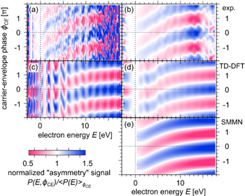
Figure 16. Carrier-envelope phase dependence of photoelectron spectra. (a), (b) Experimental data (Krüger et al 2011) shown as normalized asymmetry signal (equation (32)). Increased signal (large cut-off energy) is shown in blue, reduced emission in red. (a) Raw data, (b) smoothed over 1.5 eV and 0.5 π. Absolute phase has been adjusted to match results of the TDDFT simulation (c), (d). (c) raw data, (d) smoothing as for experiment. (e) CEP-dependent spectrum modeled by the SMMN. Figure from Wachter (2014).
Download figure:
Standard image High-resolution imageA simple estimate (Chapter 5) provides an intuitive understanding of the CEP dependence of photoemission. Assuming electron emission at the field maximum t0, the shift of the rescattered momentum distribution pr in equation (13) reduces to  with ts determined by the solution of Newton's equations for an initial momentum at the tunnel exit of p(t0) = 0 (section 5.1). Obviously, the resulting trajectories and rescattering times ts are sensitive to the CEP leading to the observed CEP-dependent shift of the high-energy part of the electron spectra. More elaborate calculations using the SMMN (section 5.2) lead to the asymmetry structure shown in figure 16(e), closely resembling the experimental and TDDFT results. Both the bent-stripe structure including the curvature and the slope of the low-energy part resulting from the interplay of the strongly nonlinear tunneling rate and the rescattering process are reproduced. For ϕCE = π (minus-cosine-pulse), rescattering is strongest, leading to the largest cut-off energy and largest number of electrons at high energies (blue). The tunneling probability at the maximum preceding the minus-cosine peak is, however, smaller than, e.g. for a plus-sine-pulse, for which, in turn, a smaller rescattering energy is found. Overall, this interplay underlies the bent-stripe pattern in the CEP dependence.
The near-perfect agreement between model calculations and experimental data in combination with simulations of pulse propagation (phase shift of the near-field at the surface induced by the nanostructure) opens up the possibility to determine the absolute phase of ultrashort laser pulses by recording photoelectron spectra in laser-nanotip interactions (see section 10.1).
8.2. Waveform control of sub-optical-cycle acceleration
Kinematic CEP effects in the tunneling regime  and sub-optical-cycle acceleration regime have been investigated by Piglosiewicz et al (2014). The authors used CEP-stable 16 fs 1.65 μm pulses in order to drive strong-field photoemission from a gold nanotip, with an enhanced field strength of
  . Figure 17(a) shows CEP-dependent spectra. Both the low-energy and the high-energy cut-offs of the spectrum depend on the CEP; their positions oscillate approximately out-of-phase (figure 17(b)). Classical trajectory calculations, taking into account a very small near-field decay constant, match the experimental results (figures 17(c), (d)). The waveform predominantly affects the dynamics of the accelerated electrons.
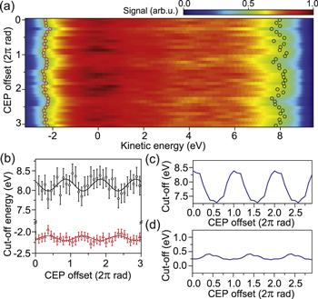
Figure 17. Waveform control of sub-optical-cycle acceleration. (a) CEP-resolved energy spectra (Au tip, 1.65μm). Clear modulation of both low-energy and high-energy cut-offs are observed, marked by red and black circles, respectively. (b) Position of low-energy cut-off (red triangles) and its high-energy counterpart (black circles) as a function of the CEP. Solid curves represent sinusoidal fits; the two cut-off energies oscillate almost fully out-of-phase. (c), (d) Classical trajectory calculation results for both cut-offs. Adapted by permission from [Springer Nature]: [Nature Photonics] (Piglosiewicz et al 2014), Nat. Phot. 8, 37.
Download figure:
Standard image High-resolution imageAnother route to explore the temporal dynamics in the sub-optical-cycle acceleration regime has been implemented by Echternkamp et al (2016b). At the long-wavelength frontier, the authors employed ultrashort laser pulses at 8.7 μm. Then, only one optical cycle contributes to the emission; a single wavepacket is generated and immediately accelerated in the near-field without any further interaction with the surface. With the knowledge of the dynamics of the electron inside the near-field, the spectral shape of the emitted photoelectrons can be directly mapped on the sub-optical-cycle emission rate (see figure 18). The reconstructed rate agrees well with the FN tunneling rate (equation (5)), confirming its suitability to describe tunneling photoemission from metallic surfaces.

Figure 18. Reconstruction of the sub-optical-cycle emission rate. (a) Time-to-energy mapping (blue) enables the reconstruction of the instantaneous rate from the electron spectrum ((b), driven by a 8.7 μm pulse). The reconstructed rate compares well with the FN rate (gray). Adapted by permission from [Springer Nature]: [Applied Physics B: Lasers and Optics] (Echternkamp et al 2016b), Appl. Phys. B 122 (4), 80.
Download figure:
Standard image High-resolution image9. Harmonic generation
So far, we have focused on the energy spectra of the electrons photoemitted from a metal nanotip by ultrashort laser pulses. In this section, we will discuss another consequence of strong-field laser-matter interaction, namely the emission of radiation with photon energies of n · ℏω, a process known as HHG. HHG from atoms is well understood based on the three-step model. Although not experimentally demonstrated, the possibility of plasmon-enhanced gas-phase HHG has triggered extensive theoretical work (see, e.g. Yavuz et al (2012), Ciappina et al (2012), Lupetti et al (2013), Pérez-Hernández et al (2013), Wang et al (2017), Yuan et al (2018), for the influence of plasmonic effects on field enhancement for nanotips see Chapter 2). Three-step models of HHG from bulk solids in momentum space have only recently been proposed (see, e.g. Golde et al 2008, Vampa et al 2014, Higuchi et al 2014, Vampa and Brabec 2017, Chizhova et al 2017). For atoms, a high-energy cut-off at 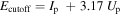 was predicted from classical trajectory analysis and confirmed in experiment. For solids and surfaces of nanostructures, the influence of collective effects, e.g. plasmon excitation, on HHG is difficult to assess. A single active electron TDSE calculation has been performed to study HHG from nanotips (Ciappina et al 2014). Here, we will use TDDFT to investigate HHG from nanotips and provide estimates for the possibility to observe the emission of high-energy photons in experiment.
To the best of our knowledge, direct HHG from nanostructures including metal tips has not been observed. The reason for this can be found by an order-of-magnitude estimate for the emission rate of HHG from a nanostructure compared to that for HHG from a gas of atoms. The number of gas atoms in the laser focus is typically about 1010, while the surface of a nanotip of radius 10 nm only contains about 5000 atoms. This huge disparity in the number of potential emitters considerably reduces the emission rate and, thus, the likelihood for the observation of HHG from isolated nanostructures. We can further estimate the order of magnitude of the linear response at the driving frequency. Modeling the metallic nanotip as a nanosphere of the same radius R as the tip, the induced dipole moment,

at the driving wavelength in linear response serves as a measure of its scattering power. The angle-integrated emitted radiation calculated from the dipole acceleration is then given by (Jackson (1999))
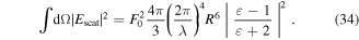
For typical ultrashort pulses employed in laser-nanotip interactions (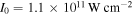 , focus size ∼1.5 μm, τ = 6.5 fs, λ = 800 nm), only about half a photon is scattered on average for the incident number of photons, in our example more than 108. This sets the scale for the results shown in figure 19. The total spectrum (
 shown for various intensities) features a strong linear-response peak at ℏω, three orders of magnitude more intense than the plateau region extending up to the plasmon energy. High-energy components of the spectrum are observed up to around
  (panel (a)), with ωp the plasma frequency and Up calculated from the locally enhanced field strength Feff. The appearance of even harmonics is a consequence of the broken symmetry at the surface. Time-frequency analysis of the emission process, i.e. a windowed Fourier transform, relates the emission times of the most intense harmonics with the recollision times of the photoemitted electrons (vertical dotted lines in panel (b)). Note that in this (nearly) free-electron gas calculation the influence of the plasmon excitation, in particular the extension of the plateau region by the plasmon energy ℏωp, is clearly visible and differs from atomic spectra. This extension can serve as an indicator for possible metal-surface and nanostructure effects.
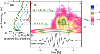
Figure 19. Simulated HHG spectra from metallic nanotips. (a) Harmonic spectra for Feff = 0.005, 0.01 and 0.018 a.u. The dielectric response of the system to a δ-kick containing all frequencies is shown in red. (b) Time-frequency analysis of emitted radiation for Feff = 0.018 a.u. The highest harmonics well above the cut-off energy of HHG in atoms are emitted in time close to the zero-crossings of the driving-laser field (c) when emitted electrons are rescattered at the surface (vertical dotted lines). Figure from Wachter (2014).
Download figure:
Standard image High-resolution imageComparison of our estimate for the linear response with the intensity of higher-order harmonics in figure 19 gives an impression of the expected photon yield. Taking for example the 7th harmonic around 11 eV photon energy and taking the reduction of the intensity of the plateau compared to the response at the driving frequency, we arrive at a yield of ∼10−3 harmonic photons per laser pulse. This small signal can only be mitigated by an increased repetition rate of the incident pulsed laser beam or the irradiation of large ensembles of nanostructures such as free-standing copper nanowires grown in polymer ion-track membranes (Maurer et al 2006) or nano-patterned arrays of doped silicon tips (Swanwick et al 2014), possibly further enhanced by superradiance effects. Very recently, the irradiation of blades has come into focus (Paschen et al 2018), enhancing the number of atoms in the laser focus and potentially boosting HHG yield by a factor of λ/R ∼ 100.
10. Applications of tip-based photoemission
A wide range of applications of pulsed nanoscale electron sources has been developed in the past ten years. Here, we turn our attention first to applications that make direct use of the sub-optical-cycle nature of the electron dynamics occurring at the source itself (Section 10.1) and then extend our scope to experiments and applications that employ the coherent electron pulses subsequent to their generation (section 10.2).
10.1. Lightwave metrology and control of electron dynamics in time and space
The work presented in the previous chapters shows that the photoemission and acceleration of electrons are field-driven processes and can be controlled by the waveform of the driving-laser field. This enables control of electric currents on the attosecond time scale, opening up pathways towards 'lightwave electronics'. Here, instead of a static field or a microwave field in conventional electronics, an optical field controls and steers electric currents at PHz frequencies (Goulielmakis et al 2007, Krausz and Ivanov 2009, Krausz and Stockman 2014) for which single-cycle optical pulses can be achieved (Manzoni et al 2015, Hassan et al 2016). In order to make use of the control capability, a nanoscale device is necessary since the typical speed of an electron in a metal is given by the Fermi velocity, which is of the order of nanometer per femtosecond. Initial work towards a vacuum nano-gap diode driven by a 5 fs, 800 nm laser pulse was performed by Higuchi et al (2015), who approached two tungsten nanotips with different radii to a distance of about 200 nm and measured the photocurrent crossing the gap from the sharper tip (serving as an anode) to the blunter tip (serving as a cathode). The time resolution is of the order of hundreds of femtoseconds corresponding to the gap crossing time. The first sub-optical-cycle-resolved study of a laser-driven nano-gap diode was performed by Rybka et al (2016). CEP-stable 6 fs pulses at a central wavelength of 1.3 μm were generated and focused on a nano-gap antenna structure fabricated from gold with electron-beam lithography (see figures 20(a) and (b)). The gap was only 8 nm wide, which is why the experiment could be performed in ambient air and at room temperature. Scanning the CEP of the 1.4-cycle pulses leads to the generation of a net current through the gap and also influences its direction and magnitude. The mechanism here is the strong dependence of tunneling photoemission on the waveform of the pulse. Current pulses generated from half-cycles with negative sign can exceed those generated from half-cycles with positive sign and vice versa. It is the asymmetric light field that breaks the symmetry and leads to a net current flow. Waveform-induced forward-backward symmetry breaking can be enhanced by symmetry breaking of the nano-electrode's geometry. Putnam et al (2017) have reported on an experiment where strong-field photoemission from nanotriangle or nanorod arrays is triggered by 10 fs, 1.2 μm pulses and detected by a large collector electrode at a distance of about 5 μm. The authors find a detectable CEP-dependent current only for the nanotriangle array since nanorods exhibit forward-backward symmetry, while at nanotriangles a single sharp feature contributes to the photoemission process. In the latter case, only every other half-cycle produces photoelectrons, significantly enhancing CEP effects.

Figure 20. Lightwave electronics and coherent control of electric currents. (a) Sketch of a lightwave-driven nano-gap antenna device in air. The electric field F of a CEP-stable 6 fs laser pulse at 1.3 μm (red and blue curves) drives a current I between two gold nanoelectrodes separated by an 8 nm gap (inset: scanning electron micrograph). The waveform asymmetry introduced by the CEP determines the magnitude and direction of the current, which is measured by a high-precision amperemeter. (b) Average current expressed in pA and electrons per pulse as a function of the CEP (red solid curve). The gray solid curves represent eight subsequent measurements used for averaging. Waveforms corresponding to three data points are indicated. Adapted by permission from [Springer Nature]: [Nature Photonics] (Rybka et al 2016)), Nat. Phot. 10. (c) Sketch of a coherent control experiment of above-threshold photoemission from a tungsten nanotip using two colors (1.55 μm and a weak admixture of its second harmonic). The ω − 2ω delay is the experimental control parameter. (d) Total emission current as a function of sub-optical-cycle delay. The current is modulated by up to 97.5%, corresponding to an almost perfect switch-on-off scenario. Reprinted figure with permission from Förster et al (2016), Copyright (2016) by the American Physical Society. (e) Illustration of the underlying physical mechanism: two-path quantum interference leads to a modulation of the total current. A resonance located at an intermediate energy level (dashed line) mediates the interference (EF: Fermi energy. Weff: Schottky-lowered work function).
Download figure:
Standard image High-resolution imageSymmetry breaking by the waveform of the light field can also be achieved using two-color pulses. Working in the multiphoton regime, Förster et al (2016), Paschen et al (2017) and Seiffert et al (2018) used 74 fs, 1.55 μm pulses with a weak admixture of the second harmonic and measured electron spectra and total current as a function of the two-color delay (see figures 20(c)–(e)). They found strong sinusoidal oscillations of the total current with a periodicity of Topt/2 and a modulation depth of up to 97.5%. The experimental results are consistent with two-path quantum interference where one path includes the absorption of a second harmonic photon and the other includes the absorption of two fundamental photons (see figure 20(e)). A DFT calculation revealed a possible resonance in the SDOS, allowing for this type of quantum path interference and a high degree of coherent control. Another recent experiment explored the polarization and delay dependence of multiphoton photoemission driven by a two-color field (800 + 400 nm), but did not observe sub-optical-cycle quantum interference (Huang et al 2017).
The waveform dependence of strong-field photoemission and electron acceleration allows for the determination of the CEP of ultrashort laser pulses. Nanotip experiments enable CEP sensing, but for practical applications such as the stabilization of the carrier-envelope offset frequency or single-shot CEP measurements, the electron yield needs to be increased by several orders of magnitude, for example by using nanostructure arrays (Schenk et al 2011). The CEP of the nano-optical near-field at a nanotip is shifted by a wavelength- and geometry-dependent phase retardation with respect to the CEP of the incident pulse (see section 2.2). Therefore, spectrally resolved photocurrent measurements enable measurements of the local CEP up to a constant phase shift. Rescattered electrons are very sensitive to the CEP (see Chapter 8). Strong-field photoemission from the apex of a nanotip has been employed to measure the spatial variation of the local CEP inside a focused broadband 4 fs laser pulse at a wavelength of 700 nm as a function of longitudinal and radial position. The focal phase does not follow the behavior of the monochromatic Gouy phase, as one could naively assume, but rather shows a strong dependence on the chromatic beam properties, characterized to first order by the wavelength-dependent Rayleigh range of the beam prior to focusing (Porras 2009, Hoff et al 2017a, 2017b). The phase retardation of the near-field with respect to the incident field has been measured in a streaking experiment employing single isolated attosecond XUV pulses (Förg et al 2016), implementing attosecond nanoplasmonic streaking (Stockman et al 2007, Süßmann and Kling 2011). Electrons released by XUV photoemission are streaked by the near-field generated by an ultrashort infrared pulse enabling its reconstruction.
Rescattered electrons also encode the strength of the light field, which led to their creation and acceleration. For δ ≫ 1 (see Chapter 7), the rescattering cut-off encodes the intensity of the near-field. Spectral measurements have been employed to determine the near-field enhancement at nanotips (Thomas et al 2013, Krüger et al 2014) and nanorod and bow-tie arrays (Rácz et al 2017, 2018). For δ ∼ 1, the near-field decay must be taken into account, enabling a vectorial reconstruction of the near-field (Park et al 2013). In addition to spectrally resolved studies, measuring photoemission rates enables rough estimates of the strength of the near-field, both in the multiphoton regime (Ropers et al 2007c, Grubisic et al 2013) and the transition regime to strong fields with its 'kink' around γ ∼ 1.
Superimposing strong-field photoemission of a nanotip with a low-frequency sub-two-cycle THz field adds a slowly varying time-dependent electric field to the process (Herink et al 2014, Wimmer et al 2014). Controlling the time delay between the THz pulse and the strong infrared driving pulse controls the kinetic energy distribution of the resulting electron pulse, which can be used to fully suppress photoemission. A systematic experimental and theoretical study revealed the strong potential of spectro-temporal electron pulse shaping using a combination of static and THz fields (Wimmer et al 2017), in analogy to THz manipulation of free-electron beams (Kealhofer et al 2016).
Most experiments described in this article are concerned only with electron emission from the tip apex in the forward direction, but the geometry and surface structure of a nanotip allow manipulation of the spatial emission pattern by means of laser polarization and incidence angle. Such manipulations were reported by Yanagisawa et al (2009, 2010, 2013) for a tungsten tip (R ∼ 100 nm) in the photofield emission regime. The interplay between the locally varying work function, corresponding to different facets on the hemispherical tip apex, and the local strength and direction of the near-field enables a high degree of directional emission control. In addition, emission from facets with low local work function enables spatial double-slit experiments with polarization-controlled fringe contrast (Yanagisawa et al 2017).
10.2. Laser-triggered nanotips as coherent source of electron pulses
Pulsed coherent electron beams open up a wide range of applications in ultrafast electron diffraction, microscopy and matter-wave quantum optics. Nanotips are highly coherent electron sources not only when operated in DC field emission but also when triggered by ultrashort laser pulses. The virtual source radius reff (also called effective source size) of a nanotip is defined as the radius of a virtual incoherent emitter that resembles the coherence properties of the tip. The smaller reff, the more the tip acts like a (fully coherent) point source of electrons. In DC field emission, reff can be in the order of 1 nm and even less for tips with radii of the order of 10 nm (Spence 2013). The transverse coherence length is defined as the size of coherent illumination of a sample by the electron beam and is inversely proportional to reff. The coherence properties of laser-triggered electron beams from a nanotip were investigated for single-photon photoemission assisted by the Schottky effect with kinetic energies in the order of 50 eV (Ehberger et al 2015). Diffraction from a CNT placed close to the nanotip was used to determine reff ≃ 0.8 nm for a tip radius in the order of 10 nm, which compares well with reff ≃ 0.55 nm for DC field emission. The ratio K of transverse coherence length to beam size was found to be 0.36—the highest reported value for a laser-triggered electron source. Comparable results have been found in an ultrafast transmission electron microscope (UTEM) with a nanotip triggered by two-photon photoemission (Feist et al 2017); at 200 keV electron energy, the authors find K ≈ 0.11. Compared to photocathode sources used for ultrafast electron microscopy (Reed et al 2009), nanotip emitters offer superior coherence. Fully coherent femtosecond electron sources might result from laser-driven single-atom tips. These tips end in a single atom and are known to be fully coherent in DC field emission operation (Fink 1986, Fu et al 2001, Hommelhoff et al 2009).
Laser-triggered nanotip-based electron guns require electron optics to deliver the electrons on the sample. Point-projection microscopy (PPM) is the simplest electron imaging technique and relies on the nanometric size of the tip with respect to a spatially resolving electron multiplier serving as a screen (Fink et al 1990). A sample is placed very close (sub-μm scale) to the tip and the electron trajectories emanating from the tip apex lead to a magnification of the sample on the screen of up to 106 allowing for ∼1 nm-resolution holographic imaging of single molecules in PPM (Longchamp et al 2017). Several pioneering experiments explored implementations of time-resolved PPM using laser-triggered nanotips (Quinonez et al 2013, Bainbridge et al 2016, Müller et al 2016), with one experiment reporting the observation of photo-excited currents in a nanowire with 50-fs resolution (Müller et al 2015). At close tip-sample distances, it is desirable to separate the optical excitation of the tip from that of the sample. This can be achieved using grating-coupled surface plasmon nanofocusing (Schröder et al 2015a, Vogelsang et al 2015, Müller et al 2016) or a metal-coated fiber tip (Casandruc et al 2015).
The integration of a laser-triggered nanotip into an electron gun assembly usually requires a combination of a suppressor electrode followed by acceleration and focusing electron optics (Paarmann et al 2012, Hoffrogge et al 2014, Bormann et al 2015, Storeck et al 2017). Due to matter-wave dispersion of free electrons on the way to the sample, electron pulse durations are limited to about 40 fs. Temporal electron bunch compression to femtosecond durations, even up to the formation of attosecond pulse trains, can be achieved through interactions with microwave cavities, with near-fields at nanostructures and material discontinuities in the THz and optical domain (Kealhofer et al 2016, Hassan et al 2017, Kozák et al 2017, Priebe et al 2017, Morimoto and Baum 2018) and with the field of high-intensity optical traveling waves (Kozák et al 2018a, 2018b). Sub-keV electron pulses from nanotips have been applied for low-energy electron diffraction (Gulde et al 2014, Müller et al 2015, Storeck et al 2017, Vogelgesang et al 2018). The integration of a laser-triggered nano-emitter has been demonstrated in a scanning electron microscope (SEM) (Yang 2010, Kozák et al 2018a) and in a UTEM reaching electron energies in excess of 100 keV (Caruso et al 2017, Feist et al 2017, Plemmons and Flannigan 2017, Houdellier et al 2018).
Nanotip photoemission is also explored for source applications in electron accelerators because of its high-brightness B. The brightness is defined as  , where β is the beam's full opening angle and j is the total emission current. A laser-triggered nanotip can serve as the electron source in a multi-stage dielectric laser accelerator, requiring high-brightness electron beams (Breuer and Hommelhoff 2013, Peralta et al 2013, England et al 2014, McNeur et al 2016). In addition, conventional electron accelerators benefit from high-brightness sources of electron bunches. Fundamental emission mechanisms and beam properties of nanostructure arrays were studied in order to increase the total charge per electron bunch (see Mustonen et al 2011, Nagel et al 2013, Keathley et al 2013, Vilayurganapathy et al 2013, Swanwick et al 2014, Gubko et al 2014, Hobbs et al 2014, Dong et al 2015, Li et al 2017).
Highly coherent electron pulses from nanotips also allow for fundamental matter-wave quantum optics with free electrons in the single-electron regime (see Jones et al (2016) for a recent review). Notable is the test of the dispersionless nature of the magnetic Aharonov–Bohm effect, adding a time-dependent perspective to a basic quantum phenomenon (Caprez et al 2007, Hilbert et al 2011, Batelaan and Becker 2015). The interaction of nanotip-based UTEM electron pulses with nano-optical near-fields has enabled studies of coherent manipulation and reconstruction of electron quantum states (Feist et al 2015, Echternkamp et al 2016a, Priebe et al 2017). Recently, ponderomotive acceleration of an electron bunch in free space has been demonstrated with the help of a laser-triggered SEM (Kozák et al 2018a, 2018b). Finally, nanotips open up tests of Pauli degeneracy of free electrons (Lougovski and Batelaan 2011, Jones et al 2016) as the strong confinement of electron emission in time will lead to much higher degeneracies than the record degeneracy of 10−4 achieved with a DC field emitter (Kiesel et al 2002).
11. Conclusion
Strong-field-driven photoemission from nanotips has been developed into a powerful small-scale strong-field laboratory, revealing for the first time fundamental attosecond phenomena at the surface of nanoscale solids. The versatility of nanotips has led to a wide variety of applications, with ramifications in lightwave electronics and ultrafast material science. Now the way is open to apply advanced methods of attosecond spectroscopy to the nanoscale in order to study ultrafast phenomena at surfaces and interfaces in real time. We anticipate new and exciting research in the coming decade, enabled by the extreme localization of light and matter on the (sub-) nanometer length and attosecond time scales.
12. List of symbols
- A(t): vector potential
- α: quiver radius
- β: electron beam full opening angle
- c, C: constants
- d: dipole moment
- D: density of states
- δ: dimensionless spatial adiabacity parameter
- δn: induced charge density change
- Δϕ: near-field phase shift
- Δθ: scattering angle
- ΔWs: lowering of the surface-vacuum barrier by the Schottky effect
- e: electron charge
- Ecutoff: cut-off energy
- EF: Fermi energy
- Ekin: kinetic energy
- Ephot: photon energy
- : dielectric function
- 0: dielectric constant
- f: prefactor to tunneling rates
-
 : light field envelope function
 - F(t): time-dependent optical near-field
- F0: electric field amplitude
- FDC: DC field
- Feff: effective field amplitude including field enhancement
- γ: Keldysh parameter
- ℏ: (reduced) Planck constant.
- I0: cycle-averaged peak intensity
- Ieff: effective cycle-averaged peak intensity including field enhancement
- In: coefficients for the strong-field approximation
- Ip: atomic ionization potential
- j: electric current
- jFN: field emission current
- k: wave number (electron or photon)
- kr: field reduction factor
- K: ratio of the transverse coherence length and electron-beam size
- lF: near-field decay constant
- λ: wavelength
- λF: Fermi wavelength
- λTF: Thomas–Fermi screening length
- m: electron mass
- nmin: minimum required number of photons to overcome the work function
- n(z, t): charge density
- ω: angular frequency
- ωp: plasma frequency
- Ω: solid emission angle
- p: momentum
- P: electron spectrum
- ϕCE: carrier-envelope phase
- ϕi: non-interacting pseudo-single-particle wavefunctions
- ψ: wavefunction
- ψd: direct wavepacket
- ψr: rescattered wavepacket
- reff: effective source radius
- R: tip radius of curvature
- S: action
- σp: width of momentum distribution
- t: time
- t0: ionization time
- ts: recollision time
- Topt optical-cycle duration
- θ: tip half-opening angle
- Θ: Heaviside function
- Up: ponderomotive energy
- v: velocity
- vF: Fermi velocity
- V: potential energy
- Veff: effective potential
- Vext: external potential
- Vsurf: surface potential
- w: emission rate
- W: work function
- Wi: electron binding energy
- ξ: field enhancement factor
- z: reaction coordinate along surface normal
- zD: detector position

13. List of acronyms
- 2PPE: two-photon photoemission
- APT: atom probe tomography
- ATI: above-threshold ionization
- ATP: above-threshold photoemission
- BEM: boundary element method
- CEP: carrier-envelope phase
- CNT: carbon nanotube
- CTMC: classical trajectory Monte Carlo
- DFT: density functional theory
- SDOS: surface density of states
- FDTD: finite-difference time-domain
- FN: Fowler and Nordheim
- FWHM: full width at half maximum
- HHG: high-harmonic generation
- IR: infrared
- LSP: localized surface plasmon
- MCP: micro-channel plate
- MPP: multiphoton photoemission
- OAP: off-axis parabolic mirror
- PPM: point-projection microscopy
- SEM: scanning electron microscope
- SFA: strong-field approximation
- SMMN: simple man's model for nanotips
- SNOM: scanning near-field microscopy
- TDDFT: time-dependent density functional theory
- TDSE: time-dependent Schrödinger equation
- TERS: tip-enhanced Raman scattering
- TOF: time of flight
- UTEM: ultrafast transmission electron microscope
- UV: ultraviolet
- VMI: velocity map imaging
- XUV: extreme ultraviolet
Acknowledgments
MK and PH acknowledge funding through ERC Consolidator Grant 'Near Field Atto', DFG SFB 953, DFG SPP 1840 'QUTIF'. CL, GW and JB thank the Austrian Science Fund (FWF), project numbers SFB-041 ViCoM, SFB-049 NextLite, and doctoral college W1243, and also the COST Action CM1204 (XLIC) and the IMPRS-APS for support. Calculations were performed using the Vienna Scientific Cluster (VSC). MK acknowledges financial support from the Minerva Foundation and the Koshland Foundation.