
Abstract
Polar (001) and nonpolar (110) ZnO epitaxial thin films were grown on SrTiO3 substrates by the pulsed laser deposition method and the in-plane electric transport was investigated. Both films display semiconducting behavior. The polar thin films have linear I–V relations with mobility increasing almost linearly with temperature. In contrast, for nonpolar ZnO thin films, the I–V curves are symmetric and nonlinear with room temperature resistivity 30 times larger than that of polar thin films. We conclude that in nonpolar ZnO thin films the bound polarization charge induced barrier limits the carrier transport. Instead, for polar thin films, the polar effect on the in-plane transport is negligible, and the charged dislocation scattering is dominant. Our observations suggest the polar effect should be considered in the design of ZnO related devices.
Export citation and abstract BibTeX RIS
1. Introduction
ZnO is a direct wide band gap semiconductor with a high exciton binding energy (60 meV) at room temperature (RT). It has attracted substantial attention in recent years due to its wide use in a variety of applications such as UV photodetectors and sensors. ZnO crystallizes into a wurtzite structure. Along the [001] direction, layers of Zn and O atoms are stacked alternately. Because of a lack of inversion symmetry and the ionic nature of the Zn–O bond, ZnO has a strong spontaneous polarization along the [001] direction. Theoretically, the spontaneous polarization of ZnO along the [001] direction is as large as − 0.057 C m−2 [1, 2], much larger than that of GaN ( − 0.029 C m−2), another industrially important wurtzite wide band gap semiconductor [2]. In ZnO epitaxial thin films, the substrate induced strain produces extra polarization resulting from the piezoelectric effect. The total polarization would generate bound positive and negative charges on  O-polar and (001) Zn-polar surfaces, respectively. The polarity in wurtzites has significant influence on the morphology of epitaxial thin films [3–5], electrical and optical properties of heterostructures [6–9], surface chemistry [10, 11], designing and performance of devices [12–16].
On the other hand, as an important class of strongly correlated electron systems, perovskite transition-metal oxides (TMO) exhibit many exotic properties such as high temperature superconductivity, colossal magnetoresistance (CMR), and ferroelectricity. Integration of ZnO with TMO may generate new fascinating functions. SrTiO3 is one of the most important single crystal substrates on which many perovskite TMO thin films can be epitaxially grown. Fabricating epitaxial ZnO thin films on STO substrate is the first step to incorporating ZnO with TMO. Previously, successful fabrication of epitaxial ZnO thin films on STO substrates has been reported by a few authors [17–22]. However, the polarity dependent electric transport of ZnO/STO thin films has not been comparatively investigated, which is an important issue for its applications in solar cells and liquid crystal displays. In our work, we prepared polar and nonpolar ZnO films on STO substrates and studied the influence of polarity on their electric transport.
2. Materials and methods
100 nm thick ZnO thin films were grown by a pulsed laser deposition (PLD) method from a target sintered by pure ZnO (99.99%) powder with a substrate temperature of 700 °C and oxygen pressure of 2 Pa. The 5 mm long and 3 mm wide substrates were cleaned in acetone and ethanol alternately by ultrasonic cleaning before being mounted in the vacuum chamber. The base pressure of the deposition chamber was 5 × 10⁻⁴ Pa. The purity of oxygen gas used in the experiments was 99.999%. A KrF excimer laser (Lambda Physik LPX 300) with wavelength of 248 nm was used, and the energy density on the target is about 1 J cm−2. After deposition, the films were cooled to 600 °C at a rate of 5 °C min−1. Then the growth chamber was filled with oxygen to 1 atmosphere, and the films were annealed at 600 °C for 0.5 h, followed by cooling to room temperature (RT) at a rate of 5 °C min−1. The crystallinity of as-grown ZnO films was characterized by x-ray diffraction (XRD, Rigaku, D/max-RB, Cu Kα). The surface morphology and microstructure were observed by atomic force microscopy (AFM, Digital Instruments, MultiMode Nanoscope III). The atomic stoichiometry was measured by a scanning Auger nanoprobe (PHI 700, Hong Kong). A four-probe method was used to measure the resistance and I–V characteristics of the films in the temperature range from 80 to 300 K. Four parallel rectangular silver electrodes with a size of 0.5 mm × 3 mm were deposited by sputtering on ZnO films. In order to avoid the possible Joule heating during the transport measurements, the resistance was measured by applying a pulsed electric current of 1 μA with a time interval of 10 s between the two subsequent pulses. The I–V curves were measured by applying a pulsed dc voltage with an interval of 12 s. The measurements of the carrier concentration and Hall mobility were performed through the Van der Pauw method. The sample is rectangular with a size of 5 mm × 3 mm . Four circular silver electrodes with a diameter of 0.3 mm were sputtered at the middle of the four side edges of the sample.
3. Results and discussions
θ–2θ and ϕ-scans of XRD (not shown here) indicate that as-prepared ZnO thin films on (110) STO substrates are singly (001) oriented with the relations of ZnO[110] ∥ STO[001] and ![$\mathrm{ZnO}[1\bar {1}0]\parallel \mathrm{STO}[\bar {1}1 0]$](https://content.cld.iop.org/journals/0953-8984/24/29/295801/revision1/cm425077ieqn36.gif) in the film plane. While on (001) STO substrates, (110) orientated ZnO thin films are fabricated with in-plane orientation of either ZnO [001] ∥ STO[110],
in the film plane. While on (001) STO substrates, (110) orientated ZnO thin films are fabricated with in-plane orientation of either ZnO [001] ∥ STO[110], ![$\mathrm{ZnO}[1\bar {1}0]\parallel \mathrm{STO}[\bar {1}1 0]$](https://content.cld.iop.org/journals/0953-8984/24/29/295801/revision1/cm425077ieqn38.gif) or
or ![$\mathrm{ZnO}[0 0 1]\parallel \mathrm{STO}[\bar {1}1 0]$](https://content.cld.iop.org/journals/0953-8984/24/29/295801/revision1/cm425077ieqn39.gif) ,
, ![$\mathrm{ZnO}[\bar {1}1 0]\parallel \mathrm{STO}[1 1 0]$](https://content.cld.iop.org/journals/0953-8984/24/29/295801/revision1/cm425077ieqn40.gif) . These results are consistent with previous observations [17–22].
. These results are consistent with previous observations [17–22].
Figure 1 shows the AFM images of as-prepared ZnO thin films. For (001) ZnO thin films, the uniform grains are densely packed, implying a three-dimensional island and columnar growth mode as proposed by Bellingeri [19]. The root-mean-square (rms) roughness of the surface is 4.38 nm. The enlarged view of the image shows that the grain looks polygon-shaped, and the contact angle at the grain boundaries is near to 120°. In contrast, the (110) orientated ZnO film is covered by brick-like grains with two perpendicular configurations, in accord with the XRD observations. The surface rms roughness is 2.14 nm. The presence of two grain configurations with 90°-rotation to each other is favorable to release the strain induced by lattice mismatch between the ZnO thin film and STO substrate. Thermodynamically, the orientation and morphology of ZnO thin films are determined by the total free energy, including strain energy, surface energy, and electrostatic energy due to the polar character of ZnO. Considering the electrostatic energy produced from the bound polarization charges on the opposite (001) and  surfaces, we believe that the long side of the brick-like grains of nonpolar (110) ZnO films is parallel to the c-axis of ZnO.

Figure 1. AFM images of (a) (001) ZnO films on (110) STO (5 μm × 5 μm); (b) (110) ZnO films on (001) STO (1 μm × 1 μm). Inset of (a): expanded view of (a) (650 nm × 650 nm).
Download figure:
Standard imageShown in figure 2 is the temperature dependent resistivity of polar and nonpolar ZnO thin films. Both films exhibit semiconducting behavior. The in-plane resistivity of nonpolar (110) ZnO films (ρnp) is much larger than that of polar (001) films (ρp) in the whole temperature range investigated. At room temperature, ρnp is about 2.27 Ω cm, 30 times larger than that of ρp (0.074 Ω cm). At 100 K, ρnp/ρp ≈ 280. It is known that the n-type carriers in unintentionally doped ZnO originate from the self-doping of oxygen vacancies, or zinc interstitials, which is sensitive to the film growth conditions, especially oxygen vacancies in PLD fabrication. Comparison studies indicated that in the low carrier density range the carrier mobility in ZnO ceramics, polycrystalline and epitaxial thin films is much lower than that in single crystals due to the dominant scattering contribution from the grain boundaries [23]. In our case, both polar and nonpolar ZnO films were prepared simultaneously under the same conditions. The oxygen concentration in both films should be similar, which was proved by our AES measurement (not shown here). The large difference in resistivity may result from the different carrier scattering mechanisms.
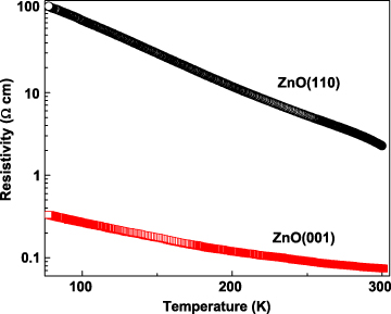
Figure 2. Temperature dependent resistivity of ZnO thin films on STO substrates.
Download figure:
Standard imageIn order to shed light on the effective transport process, the temperature dependent carrier concentration and Hall mobility of polar ZnO films are presented in figure 3(a). For nonpolar thin films the resistance is too large so that the Van der Pauw measurement cannot be accurately performed. It is seen from figure 3(a) that the carrier density of the polar ZnO thin films is weakly temperature dependent. From 20 to 300 K, the carrier density only increases from 2.57 × 10¹⁸ to 2.99 × 1018 cm−3. However, in the same temperature range the Hall mobility is increased from 4.7 to 31.2 cm2 V −1 s−1, within the range of published values in literature for doped and undoped ZnO thin films with similar electron density fabricated by magnetron sputtering and PLD [23]. But its almost linear increasing dependence on temperature is unexpected. It is worth pointing out that we have fabricated and measured several pairs of films. All the results presented in the manuscript are consistent and reproducible. In undoped ZnO single crystals, Look et al [24] observed a peak on the carrier mobility–temperature curve. Below and above the peak temperature the mobility was decreasing. They found that several electron scattering mechanisms, including polar optical-phonon scattering, acoustic-phonon scattering both through the deformation potentials and through piezoelectric interactions, and ionized-impurity scattering, contributed to the electric transport. For ZnO thin films, comprehensive studies on the carrier mobility–concentration relations indicated that at large carrier density ionized-impurity scattering governs the transport, while at low carrier density grain barriers limit the carrier mobility [23, 25, 26]. Around the carrier density of 1019 cm−3 the electron–plasmon interaction may play a significant role [27]. However, none of these mechanisms alone can explain the measured linearly increasing mobility as a function of temperature. On the other hand, theoretical calculation showed that electron scattering by charged dislocations could yield mobility proportional to the temperature [28]. It is interesting to note that although dislocation scattering seems to be a natural scattering process in semiconducting thin films, this scattering process is rarely used to explain the carrier transport behavior in transparent oxide thin films. In our case taking account of the lattice mismatch between the ZnO and underlying STO substrates together with the polar nature of the ZnO structure, the existence of charged dislocation is inevitable, especially in the region of grain boundaries. It is reasonable to ascribe the linearly increasing dependence of carrier mobility on temperature to the scattering from the charged dislocations in ZnO thin films.

Figure 3. (a) The carrier density (black squares) and mobility (red circles) as a function of temperature; (b) I–V curves at different temperatures for polar ZnO(001) thin films.
Download figure:
Standard imageIn order to clarify further the transport mechanism, the current–voltage (I–V) curves were measured. In contrast with the linear I–V curves of polar ZnO(001) thin films shown in figure 3(b), all I–V curves for nonpolar films at temperatures from 80 to 300 K are slightly but clearly nonlinear and symmetrical with respect to positive and negative bias, as typically shown in figure 4. Obviously, the nonlinearity does not come from the electrode–film contacts, because the I–V curves were measured by the four-probe method. By comparison with the linear I–V relations for polar films, the nonlinearity in the I–V curves of nonpolar thin films should originate from the regions of grain boundaries or domain boundaries. The conventional back-to-back double Schottky junction model appropriate for describing the non-ohmic voltage dependent resistance of bulk polycrystalline ZnO [29, 30] cannot physically fit our experimental data. Instead a simple Schottky thermionic emission model fits our data very well. Taking account of the morphology and polar character of (110) ZnO thin films (figure 1(b)), a layer of negative bound polarization charges on the Zn surface would lead to down bending of energy bands on both sides of the surface, as schematically shown in the inset of figure 4(a). Due to the probable existence of a larger density of defects at grain boundaries between perpendicular grains, the depletion width inside the grain (W1) is much larger than that at the grain boundary (W2). External applied voltage mainly drops across the depletion region inside the grain. In this sense, this barrier can be approximated as a single Schottky barrier. In contrast, on the opposite O surface the positive bound polarization charges would result in an electron accumulation region. As a result, along the current direction, each pair of adjoining perpendicular grains would have a single Schottky barrier. If the carrier transport is limited by the barrier, then the current can be expressed by
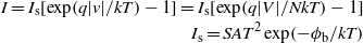
where q, v, k, T, N, S, A, ϕb are, respectively, electron charge, voltage drop across a single barrier, Boltzmann constant, absolute temperature, number of perpendicular grain pairs between voltage electrodes, cross-section area of flowing current, Richardson constant (A = 36 A cm−2 K−2 for ZnO [31] ), and barrier height. The above equations fit our data fairly well as plotted by red solid lines in figure 4(a). The extracted barrier number N is approximately 9500, in agreement with the estimation number of perpendicular grain pairs between the two voltage electrodes with 1 mm spacing found through AFM images. The calculated barrier height ϕb as a function of temperature is drawn in figure 4(b). At RT ϕb is 0.218 eV, corresponding to a bound polarization charge density of 0.0040 C m−2. This value is much smaller than the theoretical value 0.057 C m−2, but is comparable to the difference in Schottky barrier heights on Zn-polar and O-polar ZnO surfaces [9].
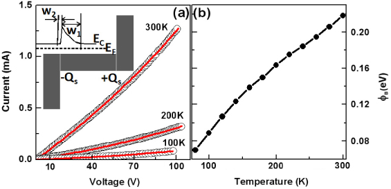
Figure 4. (a) Typical I–V curves of (110) ZnO/(001) STO thin films. Symbols are for measured values and red solid lines for fitting curves. Inset: schematic demonstration of a pair of perpendicular grains and the energy band bending near to the Zn-polar surface due to bound polarization charges Qs. EC and EF represent the bottom energy of the conduction band and the Fermi energy, respectively. W1 and W2 stand for the respective widths of the depletion region in the grain and grain boundary. (b) Calculated Schottky barrier heights at different temperatures.
Download figure:
Standard imageHowever, in polar ZnO thin films, the bound polarization charges are located on the surface and film–substrate interface. The polar effect on the in-plane electric transport is small, which is consistent with its lower resistivity and linear I–V curves.
4. Conclusions
We investigated the electric transport of the polar (001) and nonpolar (110) epitaxial ZnO thin films prepared on STO substrates by the PLD process. For nonpolar ZnO films, the potential barrier induced by the bound polarization charges on the Zn-polar surface limits the carrier transport, leading to the nonlinear I–V curves. In contrast, for polar thin films, the polar effect is negligible. Instead, the carrier scattering from the charged dislocations is dominant, resulting in the linear I–V behavior and lower resistivity. Our results suggest that the polar effects of ZnO should be considered in the future device design.
Acknowledgments
We acknowledge the financial support from the National 973 Project of China (Grant Nos 2011CB921904, 2012CB927402), National Natural Science Foundation of China (Grants Nos 11074142, 11021464), Key Project of the Chinese Ministry of Education (No. 309003), and the Tsinghua TNList Cross-discipline Foundation.