

Abstract
Multi-probe instruments based on scanning tunnelling microscopy (STM) are becoming increasingly common for their ability to perform nano- to atomic-scale investigations of nanostructures, surfaces and in situ reactions. A common configuration is the four-probe STM often coupled with in situ scanning electron microscopy (SEM) that allows precise positioning of the probes onto surfaces and nanostructures enabling electrical and scanning experiments to be performed on highly localised regions of the sample. In this paper, we assess the sensitivity of four-probe STM for in-line resistivity measurements of the bulk ZnO surface. The measurements allow comparisons to established models that are used to relate light plasma treatments (O and H) of the surfaces to the resistivity measurements. The results are correlated to x-ray photoelectron spectroscopy (XPS) and show that four-probe STM can detect changes in surface and bulk conduction mechanisms that are beyond conventional monochromatic XPS.
Export citation and abstract BibTeX RIS
Introduction
The four-probe scanning tunnelling microscopy technique combined with in situ scanning electron microscopy (SEM) was pioneered by Hasegawa and co-workers beginning in 2000 and the proceeding years after [1–3]. Since that era the technique has been commercialised and combined with numerous other in situ capabilities to achieve some incredible results on various surfaces and nanomaterials. Some notable results have refined our knowledge of defects in topological insulators using scanning tunnelling potentiometry [4], contacting and manipulating single atoms at 4 K [5], tuning of atomic chains by chemisorption [6], conductance measurements of self-assembled single layer molecules [7], identification of metallic twin grain boundaries on monolayers [8], charge transport in nanowires [9–13], and using four-probe measurements to separate surface and atomic step conductivity from bulk conductivity [14, 15].
In the area of sensors, where surface modification is typically used to induce a change in the electrical conductivity of a device, for example via adsorption [16], covalent attachment or bio-functionalisation [17], understanding the details of surface modification and correlating these details with the changes in surface conductivity due to band bending and the influence of surface states is a crucial step in realising the potential of such devices. These devices depend on changes in channel conductivity, typically this necessitates that one of the dimensions of the channel is reduced to the nanoscale at which the Debye length becomes a significant fraction of the relevant dimension. This is now commonly achieved by incorporating semiconductor nanostructures such as nanowires, nanosheets and more exotic structures into these devices.
However, when studying surface modification, there exist challenges in applying standard surface science methods to nanostructures such as free standing nanowires, likely due to the complications encountered when dealing with samples varying significantly from the semi-infinite 2D sheets best suited for relatively large area surface averaging techniques such as XPS, FTIR, Raman and ellipsometry. Electrical conductivity measurements of nanostructures which are inherently surface sensitive have become routine using lithography and multiprobe STM; however, studies of surface modification using established techniques are complicated by the morphology and dimensions of the nanostructures. Conversely, large area surface science techniques have matured around the study of semiconductor single crystals but true surface sensitive conductivity measurements on bulk substrates using micro four point probe remain rare [18].
For an idealised collinear four point probe measurement, the measured bulk resistance is inversely proportional to the contact spacing, whereas the surface resistance is independent of contact spacing [19]. Therefore, local surface sensitive conductivity measurements can be made on macroscale semiconductor single crystals provided the current probe contact spacing is made sufficiently small. Accurate sub-micron positioning of sharp probes made possible by multi-probe STM/SEM allow flexible surface sensitive conductivity measurements to be made without the need for advanced and permanent lithographic processing or the fabrication of monolithic microscale four-point probe devices.
Here we present four-point probe surface sensitive conductivity measurements conducted on a ZnO single crystal modified via simple surface plasma treatments. The four-point probe conductivity measurements are compared with valence-band and core-level XPS in order to validate the effects of these treatments on surface conduction.
The results show that correlation of surface modifications on relatively well understood, highly ordered and readily characterisable single crystal substrates with surface sensitive electrical conductivity measurements are possible. In addition, the multi-probe technique is shown to provide invaluable insight's when studying changes in surface electrical conductivity that are relevant when device dimensions are reduced down towards the nanoscale.
Zinc oxide (ZnO) is a metal oxide semiconductor with a wide band gap of 3.37 eV and high exciton binding energy of 60 meV [20]. Over recent years it has attracted a significant amount of scientific research due to its properties that include high transparency, piezoelectricity, high electron mobility and room temperature ferromagnetism [21]. ZnO can be formed into large single crystals as well as a number of nanostructures including nanowires, nanorods and nanosheets [22, 23].
ZnO crystallizes into the wurtzite structure which when viewed along the c-axis consists of alternating planes of Zn and O atoms, arranged in threefold coordinated 'double layers' separated by a single Zn–O bond. Truncation of the crystal along this axis always results in one of two polar surfaces—the Zn-polar (0 0 0 1) Zn-face or the O-polar ZnO (0 0 0  ) O-face. Due to the large electronegativity of oxygen, these polar faces have a significant ionic character and are electrostatically unstable [24, 25]. Three stabilization mechanisms are commonly proposed: (a) a fractional negative charge transfer from the O-polar to Zn-polar face; (b) a surface reconstruction which removes 25% of the surface atoms; (c) the adsorption of hydroxide (hydrogen) on the Zn-polar (O-polar) face [24–27]. In the case of the Zn-polar face, some form of condition-dependent (i.e. pH, temperature, H2/H2O partial pressure) competition between the formation of triangular islands and pits with O-terminated step edges and the adsorption of hydroxyl (OH) groups may occur [26, 27]. The O-polar face, except under rare circumstances, has been shown to exhibit an unreconstructed 1 × 1 H-termination and was therefore chosen for this study to simplify the interpretation of the electrical and XPS measurements [28, 29].
Methods
Sample preparation
ZnO single crystal grown by SurfaceNet Gmbh was cut and polished normal to the c-axis such that the (0 0 0  ) facet was uppermost on which the measurements were performed. The same wafer was cleaved into portions such that the same crystal could be used for the several treatments and measurements that were performed. Measurements were attempted on the sample fresh from the packaging but contamination prevented conductive electrical contacts to be achieved. Therefore, the as-received samples discussed in the manuscript were treated with a standard solvent clean of ultrasonically agitated acetone, methanol and IPA.
Short plasma treatments using oxygen or hydrogen gases were applied using an SPTS inductively coupled plasma system for duration of 5 min. A short exposure was chosen to limit the effect to the surface and not induce any sub-surface modifications such as defects or doping that longer, e.g. 1 h, plasma treatments create [30, 31]. Gases were introduced to the chamber at a flow rate of 100 sccm and a chamber pressure of 20 mTorr was maintained throughout the treatment. A power of 400 W was supplied by the RF generator to the chamber coil, with the platen generator switched off so as not to bias the sample.
Multi-probe STM electrical measurements
The single crystal ZnO samples were mechanically fixed to the sample plates and loaded into the UHV chamber (base pressure 1 × 10⁻¹¹ mbar) and measurements were performed at least 24 h after loading to eliminate the effect of residual photo-induced carriers. Nanoscale two-point and four-point probe measurements were carried out with an Omicron LT Nanoprobe with in situ SEM using a Keithley 2636B sourcemeter. Tungsten STM tips were etched in a solution of 2 Mol KOH using the method described by Ibe [32]. The tips were direct current annealed in UHV to remove probe oxide using the method described by Cobley et al [33] to minimise the field effects caused by shank oxide [34]. The tips where approached with the automated tunnelling feedback function. Once the 1 nA setpoint was reached the tip was retracted and the feedback function was disengaged. The tips were then manually lowered in 1 nm steps until a current above the noise was observed on to the sample to avoid local modifications to the crystal surface that may affect the resistance measurements [35].
For the two-point probe measurements the tips were lowered to the surface in this manner on to the sample surface and current–voltage (I–V) measurements were taken in the transmission line fashion. Four-point probe (4pp) measurements were performed in a linear configuration with the outer probes supplying the current and the inner sense probes measuring the voltage drop. I–V measurements were taken with the outer probes at fixed separation and the inner probe separation was varied to investigate bulk resistivity. Additionally, measurements were performed with the inner probes at fixed separation and the outer probe separation varied to investigate the surface resistivity and sensitivity of the four-probe STM technique to probe configurations [36, 37].
X-ray photo-electron spectroscopy (XPS)
The samples were analysed using a Kratos Axis Ultra-DLD photoelectron spectrometer at the University of Auckland, New Zealand, utilising monochromatic Al Kα radiation (hν = 1486.6) from a source operating at 150 W with an effective energy resolution of ~400 meV, and a take-off angle of 90°. Each sample was electrically grounded to the spectrometer to avoid sample charging and to enable the zero of the binding energy (BE) scale to be directly referenced to the Fermi level of each sample. In each case the analysis area was 700 µm by 300 µm. Survey spectra were collected at a pass energy of 160 eV, from −5 eV to 1300 eV, while high resolution spectra were collected between 526 eV and 538 eV (O 1s), from 1015 eV to 1030 eV (Zn 2p 3/2), from 280 eV to 295 eV (C 1s) and valence band (VB) spectra were collected over the range −4 eV to 15 eV. For each high resolution scan a pass energy of 20 eV was used.
Results and discussion
Four-probe STM was used to measure the resistivity of the three sample types: As-received, hydrogen plasma treated and oxygen plasma treated. The probes were manually lowered to the surface with nanometre precision in 1 nm steps until a current above the noise level was observed. Two-probe I–V sweeps (±0.2 V) were then performed between each of the probes to ensure the probe contacts were conductive and the I–V graphs were linear, a current of µA magnitude was typically recorded. It should be noted here that it was not possible to achieve conductive contacts to the sample with no cleaning treatment and as such the as-received sample underwent a standard solvent cleaning process [38].
The four contacts were aligned in a straight line, known as an in-line measurement, as shown in figure 1. Due to the highly conductive nature of the samples four probe sweeps were taken at ±0.5 mV where a current of several µA's was recorded. The current was comparable to the two-probe I–V sweeps at ±0.2 V which displays the inherent need to use the four probe configuration to overcome the contact resistance for accurate electrical resistivity measurements [37].

Figure 1. In situ SEM image from the four-probe STM instrument of a typical probe configuration used for the in-line resistivity measurements along with the four probe I–V measurement of a hydrogen plasma treated sample.
Download figure:
Standard image High-resolution imageNative ZnO is well known to be n-type conductive and although the source of this intrinsic doping remains controversial, oxygen vacancies are thought to be deep donors (~0.8–1.0 eV) below the conduction band minimum (CBM) in ZnO and therefore are not expected to provide a source of the intrinsic n-type conductivity of ZnO [39, 40]. However, Janotti and Van de Walle showed in those works that multi-coordinated H trapped inside an oxygen vacancy is predicted to be a significant shallow donor. Oxygen plasma treatment may displace hydrogen from oxygen vacancies by the filling/annihilation of oxygen vacancies. Furthermore, Brillson et al have shown that the density of oxygen vacancies can significantly increase in the near-surface region [41]. Hydrogen is well characterised as an electron donor in ZnO, with previous studies suggesting that the presence of hydrogen in the form of hydroxyl termination of the bulk lattice results in a surface electron accumulation layer (downward band bending) for bulk single crystals [42, 43].
For micro four-point probe measurements (4pp) on a bulk substrate with the probes far away from any boundaries the sample may be approximated by a semi-infinite volume of uniform resistivity material. The floating potential  in the material at a distance
  from a point contact current probe is given by [14]:
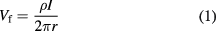
where  is the resistivity of the material. With two current probes in contact with the sample, each probe carries the same current magnitude but in opposite directions. The floating potential is then given by the difference in potentials induced by each of the current probes:
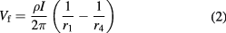
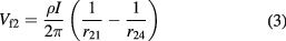
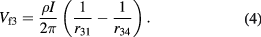
where  and
and  are the distances from probes 1 and 4, respectively. If
  , for example, represents the distance between probes 2 and 1, the floating potentials at voltage probes
  and
and  may be written as:
The potential difference between the voltage probes is then:
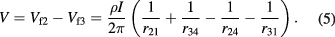
In the case of the equidistant collinear four point probe configuration, this equation simplifies to:
The four point probe resistance is defined to be:

The resistivity of the material is then given by:
where  is obtained from a linear fit to the four point measurement I–V characteristics.
Figure 2(a) shows resistivity values calculated using equation (8) (subsequently referred to as the apparent resistivity) plotted as a function of voltage (inner) probe separation with the current (outer) probes kept fixed at a separation of approximately 60 µm. A distinct change in apparent resistivity is seen following both plasma treatments. The as-received sample shows an apparent resistivity of ~0.45 Ωcm across the voltage probe separation range which is increased to ~0.6 Ωcm following oxygen plasma treatment and decreased to ~0.2 Ωcm following hydrogen plasma treatment.

Figure 2. Four point probe resistivity calculated using the semi-infinite volume approximation (equation (8)) showing resistivity as a function of: (a) voltage probe separation keeping current probe separation constant; (b) current probe separation keeping voltage probe separation constant. The graphs include resistivity error bars for the H-treated sample but the deviation in values is such that they are not apparent.
Download figure:
Standard image High-resolution imageIn the case of a bulk homogeneous and semi-infinite sample this apparent resistivity should be independent of probe spacing. Here, where a plasma treatment has been applied, local changes in resistivity would be expected to be spatially confined to the surface, invalidating the assumption of homogeneity inherent in equation (8) and resulting in a dependence of apparent resistivity on probe separation. In figure 2(a), a slight decrease in apparent resistivity is seen with reduced voltage probe spacing for all samples. This could be explained by the presence of downward band bending from a high conductivity electron accumulation layer at the surface of the as-received sample. Bands would then be modified either towards the flat band condition by oxygen plasma or further towards additional electron accumulation by the hydrogen plasma.
For reduced voltage probe separations on a bulk substrate in surface accumulation with a constant current being supplied by the outer probes, the measured voltage drop between the inner probes through the conductive surface will be less than expected for a bulk sample of uniform resistivity. This will lead to a lower 4pp resistance (equation (7)), which when multiplied by the bracketed geometric correction factors in equation (8) will result in a decrease in apparent resistivity with voltage probe separation rather than the constant resistivity expected from a homogeneous semi-infinite sample. Greater surface electron accumulation will lead to a lower apparent resistivity and consequently a greater degree of dependence on voltage probe separation. This is what is observed for the three samples, with the lower apparent resistivity hydrogen treated sample exhibiting a higher dependence on voltage probe spacing.
To investigate this further, the inner voltage probes were kept fixed at a separation of <10 µm while the outer current probes were moved. As the current probe separation is reduced, for a homogeneous sample this has the effect of confining the current to the sample surface. If this assumption of homogeneity is invalid and surface conductivity is different to the bulk, this will be reflected in the apparent resistivity calculated using equation (8). Particularly for the hydrogen plasma treated sample, reducing the current probe separation results in a decrease in apparent resistivity from ~0.35 Ωcm at 60 µm probe separation to ~0.2 Ωcm at ~18 µm before a dramatic reduction is observed to <0.05 Ωcm below 10 µm probe separation, indicating the conductivity is higher at the surface for this treatment than in the bulk, which can be explained by the effect of H-plasma treatment loading oxygen vacancies with H (figure 2(b)). A similar trend for the as-received sample is also observed but with a much smaller change from ~0.5 Ωcm at 60 µm to ~0.4 Ωcm at 5 µm probe separation. The oxygen plasma treated sample shows much higher apparent resistivity as expected for this treatment of ZnO and remains approximately constant at ~0.65 Ωcm indicating more insulating surface properties [30]. These trends of decreasing apparent resistivity with reduced current probe spacing are an expected consequence of a surface layer with higher conductivity than in the bulk. An apparent resistivity independent of probe spacing would indicate a homogeneous sample i.e. flat band conditions at the surface. The fact that all samples exhibit this downward trend suggests some degree of surface electron accumulation is present in all samples. For the as-received and hydrogen treated samples shown in figure 2(b), it is clear that surface conduction is prominent which has been previously observed by Allen et al [38] amongst others [44]. This is observed even at the largest current probe separation of ~60 µm (figure 2(b)) due to the slight difference in resistivity between samples at this spacing when compared to the 40 µm and 50 µm measurements in figure 2(a), respectively. The data also suggests that the samples were laterally homogeneous in resistivity as revealed by the measurements corresponding to the SEM images in figure 3 that show 4pp measurements on different regions of the sample with the probes orientated at ~45° to the horizontal (figure 3(b)) and with respect to the initial measurement (figure 3(a)). In these measurements the voltage probes were located at a spacing of 9.64 µm and 9.81 µm for figures 3(a) and (b), respectively, with both measurements recording a resistivity value of ~0.19 Ωcm. However, to uncover any crystallographic dependency of the resistivity comprehensive measurements would be required rotating the in-line measurements at several intervals through 60° and directly correlating the results to the crystallographic orientation of the wafer.

Figure 3. SEM images from the multi-probe instrument showing two four-probe resistivity measurements on the hydrogen plasma treated sample with the probes in (b) orientated at ~45° with respect to the probes in (a). The voltage probes are approximately at equal spacing in (a) and (b) and both measurements recorded a similar ~0.19 Ωcm resistivity.
Download figure:
Standard image High-resolution imageCoppa et al have used oxygen/helium plasma at elevated temperatures to clean 0 0 0  single crystal zinc oxide and found that it improved the gold Schottky contacts, in a similar fashion to the use of pure oxygen plasma shown by Brillson et al that reduced subsurface point defects [30, 45]. Hydrogen plasma can be used to increase the carrier concentration of ZnO single crystal by up to an order of magnitude [46] and it has been seen that hydrogenation using H plasma can reduce the defect band measured using cathodoluminescence [47]. The short plasma treatments used here are thought to have minimal effect on the subsurface defects that are usually modified by prolonged plasma treatments [30].
Core-level and valence band XPS
The effect of the surface treatments was investigated with core-level and valence band XPS. This is a useful tool for measuring near surface band bending and the resultant effect of chemical modifications on electrical properties and has been widely applied for the investigation of the bulk ZnO surface and many of the facets and nanostructures [42, 48–50].
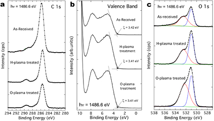
Figure 4(a) shows the C 1s peak for each of the samples and reduces significantly for the plasma treated samples. This can be seen quantitatively in table 1 that shows a reduction of 29.4% and 39.7% in surface associated carbon for the hydrogen and oxygen plasma treated samples, respectively. No significant change in the Zn 2p 3/2 peak was observed other than the Zn concentration increasing to 23.0% and 26.0% for the hydrogen and oxygen treated samples, respectively, seemingly due to the cleaning effect and removal of the adventitious carbon species present on the as-received sample. Interestingly, figure 4(b) shows the valence band edge for the three samples with no significant change in the valence band onset ζ. Although the exact carrier concentration was not known for these samples it can be estimated by referring to similar work by Heinhold et al that investigated Li concentration in ZnO crystals that had a resistivity as low as 0.3 Ωcm, similar to the samples measured here [51]. The carrier concentration of the 0.3 Ωcm crystals was ~1.1 × 1017 cm−3 (mobility ~190 cm2 V−1 s−1) so we can estimate the as received sample with resistivity of ~0.5 Ωcm has a carrier concentration of ~6.6 × 1016 cm−3.
Table 1. Compositional XPS data for the as-received, hydrogen and oxygen plasma treated samples. A significant reduction in carbon is shown for both plasma treated samples and an increase in oxygen while the cleaning effect increases the Zn 2p 3/2 signal.
| Sample | Zn (%) | O (%) | C (%) |
|---|---|---|---|
| As received: | 9.95 | 23.65 | 66.40 |
| H plasma treated: | 23.01 | 39.97 | 37.02 |
| O plasma treated: | 26.01 | 47.30 | 26.69 |
Figure 4. XPS data for the as-received sample, the hydrogen plasma treated sample and the oxygen plasma treated samples: (a) the carbon C 1s peak; (b) the valence band edge showing minimal change in ζ the valence band edge for the three samples; (c) the oxygen O 1s peak and surface-associated secondary peak displaying a significant difference on the oxygen plasma treated sample.
Download figure:
Standard image High-resolution image
When a material has a well-defined bandgap the surface band bending can be calculated directly from the valence band spectrum using linear fitting to locate the point at which the valence band emission onset occurs. XPS collects the photoelectrons emitted at energies from the Fermi level EF to the valence band (VB) maximum EV and beyond. The valence band offset (VBO) can be directly measured with a linear fit that is extrapolated from the lower binding energy edge to a line fitted to the instrument background providing the exact onset ζ = EV − EF as shown in figure 4(b) [38, 48–50]. The position of the Fermi level EF was calculated using the free carrier concentration n described above using ξ = (kT/q)ln(NC/n) relative to the conduction band (CB) minimum which gives ξ = 0.0975 eV, where the CB effective density of states [42] for ZnO is NC = 2.94 × 1018 cm−3. Therefore, the surface potential barrier VBB can be calculated from the measured ζ = 3.41 eV as VBB = Eg − ξ − ζ, where Eg = 3.37 eV is the bandgap of ZnO [20, 21] and VBB is approximately −0.14 eV (±0.05 eV). Positive values of VBB correspond to upward band bending (and consequently surface electron depletion) while negative values indicate downward band bending (and electron accumulation) and a value of −0.14 eV indicates slight downward band bending at the surface which is consistent with values between −0.2 eV and −0.4 eV that have previously been found on O-polar ZnO [38].
It is possible that by using a conventional monochromated XPS with relatively high x-ray energies (i.e. electron inelastic mean free path of ~18 Å for hν = 1486.6 eV x-rays) that small changes in ζ were not detected and the higher energy x-rays were not surface sensitive enough to detect the light surface plasma treatments that were applied. Further investigation of this with lower photon energy synchrotron x-rays with a lower inelastic mean free path and increased surface sensitivity is required but for this study it shows that conventional or monochromated XPS, used for many studies of surfaces, in this instance cannot detect changes in surface band bending that are usually associated with changes in surface conductivity [38, 48–50]. The precision of the VBO could be improved by adopting the method of Kraut et al that involves fitting an instrumentally-broadened theoretical valence band density of states to the low binding energy component of the measured VB spectra (figure 4(b)) [52, 53]. However, this is unlikely to affect the almost identical relative positions of the VBO for the as-received, H-plasma treated and O-plasma treated ZnO samples, obtained using the simpler linear extrapolation of the VB spectra low binding energy edge, that has been used in the literature for a range of oxide semiconductors [54–56]. Even so, the effectiveness of the XPS analysis and the surface treatments is revealed by the O 1s peak and surface associated shoulder shown in figure 4(c).
Examining the core-level peaks of O 1s and Zn 2p 3/2 can provide details of the surface chemistry that in this case leads to the change in surface conductivity. Table 2 shows that there is no change to the Zn 2p 3/2 peak position confirming that no change in surface band bending occurred. Examining the O 1s spectrum in figure 4(c) it is apparent there are significant differences between the samples. The O 1s spectrum contains contributions from hydroxyls, adsorbed water, surface lattice oxygen and organic molecules. The O 1s peak was fitted with two or three Gaussian–Lorentzian components [49, 57] which accurately matched the raw data. The raw peaks are shown in figure 4(c) and the associated compositional data in table 2. Here, the main O 1s peak associated with the ZnO lattice is labelled as O–Zn and the surface oxygen shoulder at greater binding energy in the O 1s peak as O–S. The FWHM of the O–Zn component for each sample was fixed at 1.1 eV which was obtained from the fitting of the as-received sample O 1s data.
Table 2. XPS Data for the three samples showing the binding energy peak positions for the O 1s bulk peak and surface associated shoulder fitted with one or two Gaussian–Lorentzian components, the full width half maximum (FWHM) of each component, and the atomic percentage along with the same data for the Zn 2p 3/2 peak.
| O 1s | Bulk O | Surface O | Zn 2p 3/2 | ||
|---|---|---|---|---|---|
OH/O2−/ |
H2O | ||||
| As-received | Peak (eV) | 531.00 | 532.50 | 534.70 | 1022.40 |
| FWHM (eV) | 1.10 | 2.00 | 2.00 | 1.80 | |
| AT.% | 46 | 48 | 6 | — | |
| H-plasma | Peak (eV) | 531.00 | 532.50 | n/a | 1022.40 |
| FWHM (eV) | 1.10 | 2.00 | n/a | 1.80 | |
| AT.% | 53 | 47 | 0 | — | |
| O-plasma | Peak (eV) | 531.00 | 532.20 | n/a | 1022.40 |
| FWHM (eV) | 1.10 | 2.00 | n/a | 1.80 | |
| AT.% | 42 | 58 | 0 | — | |
Both plasma treatments have had the effect of removing the H2O component. The presence of water on the ZnO surface under the ultra-high vacuum conditions used in XPS has been previously reported by a number of authors and is attributed to extensive hydrogen bonding between adsorbed water molecules and the terminating hydroxyl groups on the ZnO surface that the plasma treatments disrupt [42, 58, 59]. For both the as-received and hydrogen (figure 4(c)) treatments the proportion of the O–S component is similar, see table 2, and the FWHM and binding energy remain the same. Most interestingly, the increase in oxygen content on the oxygen treated sample, see table 1, has had the effect of increasing the O–S atomic percentage to 58% when compared to the hydrogen treated sample that shows no increase in O–S from the as-received sample at 47%. The increase in O–S on the oxygen treated sample coincides with a shift in the O–S peak by 0.3 eV to a lower binding energy indicating that the chemical bonds of the surface oxygen are different between the two treatments. The interpretation of the O–S peak is inherently complex due to the variety of chemical interactions that oxygen and hydrogen can have with the ZnO surface. There are a number of plausible explanations for the O–S peak (often attributed to OH groups) being greater for the oxygen treated sample: (1) there could be a different surface O contribution in addition to OH which is exhibited by the different O–S peak binding energy for the O-plasma treated sample that has shifted from the as-received and H-plasma treated samples; (2) the O-plasma treatment could increase the surface roughness and surface area which could increase the O–S signal (possibly revealing a greater contribution from H coming from the bulk of the ZnO crystal); (3) the O-plasma treatment removes/annihilates HO defects (H multi-coordinated inside an oxygen vacancy) which are predicted to be shallow donors in ZnO increasing the sample resistivity.
The chemical interaction of hydrogen introduces OH groups to the surface increasing hydroxyl formation by reaction with lattice oxygen while also reacting with adventitious carbon cleaning the surface. In comparison, oxygen plasma has the effect of reducing oxygen vacancies VO and increasing Zn vacancies VZn in the ZnO lattice near the surface. Prolonged or aggressive treatment can lead to oxygen radicals penetrating into the ZnO to form oxygen interstitials or antisite defects; however, the short treatment performed here is thought to isolate the effect to the surface as shown by the lack of change in the VB spectra [60, 61]. Hydrogen can induce surface metallicity from binding of H to the lattice oxygen  where the hydroxyls act as donors at the ZnO surface/sub-surface [38, 42, 43, 50, 58, 59, 62]. The effect on the surface conductivity is enhanced by the reaction of hydrogen with adsorbed surface oxygen ions that act as acceptors (O−, O2−) [63]. The oxygen plasma has an opposing effect reducing the number of oxygen vacancies and possibly increasing Zn vacancies which results in a reduction in the carrier concentration near the surface increasing the sample resistivity as shown by the multi-probe transport measurements [30, 49, 57, 64, 65].
The O–S peak of the as-received sample contains contributions from hydroxyls, adsorbed water, oxygen ions and organic molecules all competing for adsorption sites. On surveying the literature it is possible to associate the emission of hydroxyl groups or O2− ions on the ZnO surface to peaks that originate at a greater BE of ~2 eV from the O–Zn peak. Adsorbed H2O, adsorbed O2− and oxocarbons are generally considered to create a peak up to ~3 eV greater BE than the O–Zn [42, 66, 67]. This is shown by fitting a third peak to the as-received O 1s spectrum that is ~3.7 eV from the O–Zn peak and associated with adsorbed water. The XPS analysis of the oxygen plasma treatment shows the O–S peak is closer in BE to the O–Zn peak by ~0.3 eV than the as-received and hydrogen treated samples that could suggest an increase in surface acceptor O2− ions. The observed difference in O–S BE for the plasma treated samples is not large enough to allow fitting of 2 separate O–S peaks that clearly distinguish hydroxyls and adsorbed oxygen because the peak separation of O–S to O–Zn (table 2) is close to ~1.4 eV and often attributed to hydroxyl bonds [42, 49]. However, the other evidence provided by the electrical measurements and the detailed data of the O 1s shoulder show there are some significant differences between the samples that lower photon energy synchrotron x-rays with a lower inelastic mean free path and increased surface sensitivity could uncover.
The presence of the C–O bond from the solvent treatment on the as-received sample can have the effect of changing the O–S position to a different BE to that of hydroxyl bonds alone. However, in the analysis here the as-received sample, expected to have water and hydrocarbons on the surface, and the hydrogen plasma sample, expected to have a hydroxylated surface, show a similar O–S position at a BE of 532.5 eV but with very different electrical properties. Oxidising treatments can reduce oxygen point defects near the ZnO surface increasing the emission due to O2−/ that also appears at a similar BE as O–H bonds [67, 68]. The oxidising effect of the O plasma treatment provides the measured increase and ~0.3 eV shift in the O–S component and consequent reduction in sample conductivity [48]. The valence band spectra, electrical measurements and the detailed data of the O 1s shoulder show there are some significant differences between the samples that are only truly revealed by the multi-probe STM measurements. To explain the observed differences in the O–S components of the plasma treated samples we can look at the hydrogen treated sample and the reaction of H that will create a hydroxyl with a surface lattice O atom and act as a reducing agent cleaning and donating electrons at the surface. Hence, there is a relatively lower concentration of O shown in table 1 and O–S shown in table 2 that creates the lower resistivity and prominent surface conductivity.
Conclusions
The multi-probe measurements have been shown to reveal changes in surface conductivity that cannot be directly correlated to surface band bending as studied using monochromated XPS. The treatment of the same (0 0 0  ) bulk ZnO single crystal with relatively moderate hydrogen and oxygen plasma provided a significant change in sample resistivity and revealed surface conduction that results from surface hydrogen doping. Significant correlation using XPS with changes in sample resistivity were only detectable by the analysis of the O 1s and surface oxygen XPS components. These results have confirmed that multi-probe STM is a prime technique for detecting surface modifications that are beyond other staple surface science techniques.
Acknowledgments
AML would like to thank the support of the Sêr Cymru II fellowship scheme part-funded by the European Regional Development Fund through the Welsh Government and the facilities at the Centre for NanoHealth, Swansea University, UK. JEE would like to thank the Engineering Research Network Wales. MWA acknowledges support from the Royal Society of New Zealand Rutherford Discovery Fellowship scheme. CJB acknowledges the support of the Sêr Cymru National Research Network in Advance Engineering and Materials (NRN150). Support was provided to ARB by the Welsh Government Ser Cymru Programme and the Robert A Welch Foundation (C-0002). Support was provided by the Engineering and Physical Sciences Research Council-funded Impact Acceleration Account (grant number EP/K504002/1).