

Abstract
Two dimensional (2D) semiconductors feature exceptional optoelectronic properties controlled by strong confinement in one dimension. In this contribution, we studied interlayer excitons in a vertical p-n junction made of bilayer n-type MoS2 and few layers of p-type GaSe using current sensing atomic force microscopy (CSAFM). The p-n interface is prepared by mechanical exfoliation onto highly ordered pyrolytic graphite (HOPG). Thus the heterostructure creates an ideal layered system with HOPG serving as the bottom contact for the electrical characterization. Home-built Au tips are used as the top contact in CSAFM mode. During the basic diode characterization, the p-n interface shows strong rectification behavior with a rectification ratio of 104 at ±1 V. The I–V characteristics reveal pronounced photovoltaic effects with a fill factor of 0.55 by an excitation below the band gap. This phenomenon can be explained by the dissociation of interlayer excitons at the interface. The possibility of the interlayer exciton formation is indicated by density functional theory (DFT) calculations on this heterostructure: the valence band of GaSe and the conduction band of MoS2 contribute to an interface-specific state at an energy of about 1.5 eV. The proof of excitonic transitions to that state is provided by photoluminescence measurements at the p-n interface. Finally, photocurrent mapping at the interface under an excitation wavelength of 785 nm provides evidence of efficient extraction of such excitons. Our results demonstrate a pathway towards a 2D device for future optoelectronics and light harvesting assisted by interlayer excitons in a van der Waals (vdW) heterostructure.
Export citation and abstract BibTeX RIS
Introduction
Semiconductor p-n junctions are fundamental building blocks for electronic and optoelectronic applications. In conventional p-n junctions the two electrically active regions result from doping a single crystalline semiconductor layer and thus are covalently bonded at the interface. Several interface phenomena such as inter-atomic diffusion during growth, surface roughness, lattice mismatch, and inhomogeneous compositional distribution at the hetero-interface broaden the electronic spectrum of the heterostructure and deteriorate the device performance, especially for the very thin films. Thanks to the remarkable properties of 2D semiconductors, one can overcome such limitations and build ultra-thin van der Waals (vdW) heterostructures or even atomically thin p-n junctions [1–8]. Due to strong confinement effects, the electronic structures of these materials can be different from those of the corresponding bulk crystals [4]. Among the 2D semiconductors, transition metal dichalcogenides (TMDCs) such as MoS2 and related materials have attracted most of the attention until now [9–12]. While they are indirect gap semiconductors in their layered bulk form, they exhibit a direct gap when thinned down to monolayer thickness [1]. Moreover, TMDC monolayers of the trigonal prismatic structure type exhibit a valley degree of freedom and nonlinear optical response, due to the loss of the inversion symmetry in comparison to the hexagonally stacked bulk structure. Thus, such TMDC monolayers promise great potential in valleytronics and higher harmonics generation [13–18]. The dramatically reduced dielectric screening in the out-of-plane direction creates strongly bound excitons with exciton binding energies in the range of hundreds of meV [19, 20], and hence offers an ideal platform to investigate excitonic or many-body physics at room temperature [21–27]. Even though studying such individual 2D semiconductors has been an ongoing effort for about a decade, their combination to create vertically stacked vdW heterostructures is a more recent trend. Due to the weak vdW forces, lattice mismatch is not the most important issue for the fabrication in contrast to the epitaxial growth of 3D heterostructures. Assembling different 2D semiconductors into a hetero-stack enables the engineering of the optoelectronic properties with atomic scale precision and also creates new physical phenomena such as field effect tunneling transistors and non-volatile transparent memory devices [28–34].
One of the most interesting features of these heterostructures is the observation of interlayer excitons, which are either of charge transfer nature or coupled intralayer excitons, and in which the electron and hole of the bound electron–hole (e–h) pair are located in adjacent layers [35–39]. Here, the e–h wave function overlap is reduced in the out-of-plane direction for geometric reasons, which leads to suppressing the magnitude of the exciton oscillation strength and the exchange interaction. As a consequence, the exciton population is greatly enhanced. Due to the large spatial separation of the e–h pair, the interlayer excitons have much longer life times than those in monolayer 2D semiconductors, thus they promise potential for a wealth of interesting applications [34, 40, 41]. Such type of excitons was already studied in quantum well (QW) based systems such as GaAs–AlGaAs heterostructures. [42] However, compared to QW systems interlayer excitons in 2D heterostructures have binding energies significantly higher, which makes them stable at room temperature.
The experimental realization of interlayer excitons in vdW heterostructures involves type I and II band alignments. In a type I system, electron and hole layers are spatially separated by a barrier layer in a semiconductor/insulator/semiconductor architecture [43–45]. In a type II system, on the other hand, electrons and holes (e–h pair) are from adjacent layers, which create a conventional p-n like interface [20, 37, 38, 46]. In 2D materials such type II interfaces were shown to exhibit diode rectification and to enable band-to-band photocurrent generation [8, 47–50]. Even though the formation of interlayer excitons was demonstrated in these systems using optical spectroscopy, to the best of our knowledge, reports of such excitonic devices for optoelectronics are yet to be published. In this work, we created a type II p-n interface using n-type bilayer MoS2 and p-type few layer GaSe. The interlayer excitons are probed by measuring the photocurrent using current sensing atomic force microscopy (CSAFM).
Even though bilayer MoS2 is an indirect band gap semiconductor, the near degeneracy between indirect and direct transitions allows efficient exciton generation at the direct transition point from the K valleys in the Brillouin zone [26, 51, 52]. Moreover, a p-n junction made with bilayer MoS2 has a much higher external quantum efficiency than monolayer MoS2 [8]. Analogous to MoS2, GaSe is also a 2D semiconductor from the closely related family of metal monochalogenides. Like TMDCs, GaSe also possesses thickness dependent optoelectronic properties [53]. However, contrary to most of the TMDCs, low-lying defect states associated with Se vacancies make GaSe naturally a p-type semiconductor [54–57]. Therefore, this combination of MoS2 and GaSe is a suitable option for fabricating vdW p-n junctions from intrinsic materials, which avoids any sophisticated technological challenges encountered in doping TMDCs into a p-type material. Hence, stacking of both materials on top of highly ordered pyrolytic graphite (HOPG) creates a p-n junction. This 2D device shows very good diode rectification behaviour. The CSAFM scan at the p-n interface under illumination with light of an energy below the band gap excitation generates a spatially resolved photocurrent map that indicates the dissociation of the interlayer exciton.
Experimental details
The MoS2 used in this experiment was purchased from 2D semiconductors, USA, as bulk crystal. The GaSe crystal is of ɛ-GaSe type and was prepared by the Bridgman method. The 2D heterostructures were prepared by mechanical exfoliation. A home built stamping machine was used to control the stamping of the flakes with a lateral precision of 1 µm. After preparation of the junction, Raman spectroscopy was employed to identify the materials. An Xplora Raman spectrometer from HORIBA was used for the measurements. The sample was excited at a wavelength of 532 nm using a 100× objective and 105 µW power. The scattered light was dispersed by a 2400 l mm−1 grating and detected by an electron multiplying charged coupled detector. The thickness of bilayer MoS2 was confirmed by the difference in the Raman shift of two first order MoS2 Raman modes as well as by tapping mode atomic force microscopy (AFM) using a commercially available silicon tip and an AIST-NT scanning probe microscope. Spatially resolved photocurrent mapping was performed in CSAFM mode using the same AIST-NT system and a home built gold tip. The tip was prepared by gluing an Au wire onto a Si plate and then etching in KBr solution [58]. The I–V characteristics of the p-n junction were measured in the dark and under illumination of 638 nm and 785 nm light. Photoluminescence measurements of the heterostructure were performed using the same excitation wavelength and detector used for the Raman characterization with a laser power of 105 µW.
For the theoretical investigations, the geometric arrangement and the electronic structure at the GaSe|2ML-MoS2 interface (with GaSe at the bottom and MoS2 top layer) shown in figure 1 were investigated by density-functional band structure calculations employing a plane-wave basis set using QuantumEspresso [59, 60] and optimized, norm-conserving Vanderbilt pseudopotentials [61]. The system studied experimentally—ten layers of GaSe covered by two layers of MoS2 on HOPG—is out of reach for density functional calculations. Thus, we employed the lowest order approximation which is bilayer-MoS2 on a monolayer of GaSe. The bilayer of MoS2 is required to reproduce the relative energy of the valleys correctly [62]. For GaSe the band gap shrinks from the monolayer to the tetralayer, but for thin samples of GaSe the structure of the valence and the conduction band is hardly influenced by the number of layers and moderate strain states of few percent [63]. We chose a slab geometry, in which 15 Å of vacuum separates the periodic replica of the GaSe|2ML-MoS2 layers. The in-plane lattice parameters amount to a = 3.1602 Å (exp.) and a = 3.14 Å (calc.) for MoS2 and a = 3.755 Å (exp.) and a = 3.74 Å (calc.) for GaSe, i.e. upon direct stacking the lattice mismatch amounts to 17.2% (exp.) and 17.4% (calc.). In order to find the smallest supercell with a small, reasonable lattice mismatch, the two layered materials were rotated by 30°. Then, a (2 × 2) MoS2-layer fits on top of a (√3 × √3) GaSe layer with a lattice mismatch of about 1%, which was accommodated evenly in the two layers. The second MoS2 layer is then added with the same lateral translation state as in the thermodynamically stable bulk MoS2 phase (ABA stacking, see figure 1), such that a GaSe|2ML-MoS2 layered stack is formed. Following the recent work by Zolyomi et al [64] on gallium chalcogenides, calculations for the electronic structure were performed with the HSE06 functional for bilayer and trilayer supercells.

Figure 1. The geometry of the simulated GaSe|2ML-MoS2 system (left) together with the unit cell (right): a (2 × 2) MoS2 unit cell (bilayer, ABA stacking) approximately fits on top of a (√3 × √3) unit cell of GaSe rotated by 30°. The layer thickness is taken as the difference of the atomic positions disregarding their spatial extension. Top view of the simulated geometry (bottom left).
Download figure:
Standard image High-resolution imageResults
Figure 2(a) shows the schematic of the vdW heterostructure. The p-n junction was prepared on an HOPG substrate acting as the bottom contact for the 2D device. Since the surface of GaSe oxidizes in air rather quickly [65], a few layers of the materials were considered for the heterojunction formation. In order to minimize the oxidation effect, the heterojunction was prepared in less than two minutes of exposure of the GaSe flake to air. In this way, we can protect a large amount of defect-free surface of freshly cleaved GaSe by covering it with bilayer MoS2 film [66], as oxidation starts at dangling bonds at the edges and at defect sites on the surface. Therefore, oxidation of GaSe is likely to have minimal effect on interlayer exciton formation due to the protective capping with the MoS2 layer. Moreover, it was already demonstrated by several groups [43–45], that interlayer excitons can form between two monolayer TMDCs separated by an insulating layer, which in our case would be a monolayer oxide. A home built Au tip was used as the top contact for the electrical characterization. The tip was used for both I–V measurements in a point contact geometry and for current mapping of the p-n interface. Figure 2(b) presents the optical image of the heterostructure with an enlarged image of the area of interest (AOI) in the inset. Conventional micro-Raman spectroscopy was performed to identify the heterostructure and to determine the thickness of the MoS2 film. GaSe has three Raman modes around 132 cm−1 ( ), 211 cm−1 (E2g) and 306 cm−1 (
 ) [65], while MoS2 has two prominent Raman modes around 385 cm−1 (E2g) and 405 cm−1 (A1g). The Raman spectra of the heterostructure (figure 2(c)) reveal the features of both materials, which confirms the formation of a weakly interacting heterojunction. To determine the MoS2 film thickness, the two Raman features of MoS2 were fitted with a Voigt function as presented in the online supplementary information (figure SI1) (stacks.iop.org/JPhysCM/31/114001/mmedia). The frequency difference between the two main MoS2 features is 23.6 cm−1 thus characteristic for bilayer MoS2 [67]. A height profile determined by tapping mode AFM is displayed in the inset of figure 1(c). The height profile is taken along the dashed line shown in the inset of the optical image in figure 2(b). Here, the thickness of the bilayer MoS2 is determined to be (1.7 ± 0.3) nm, which compares well with the value of 1.4 nm estimated on the basis of the crystal structure. The slightly higher thickness value of the flake could be due to absorbents such as water or organics accumulated on the surface in air.

Figure 2. Schematic (a), optical image (b), and Raman spectra (c) of the heterostructure. A home built Au tip is used for the electrical characterization. The height profile of the bilayer MoS2 flake is presented in the inset of (c) taken along the dashed line shown in the inset of (b) using tapping mode AFM. The Raman spectra of bulk GaSe is presented in (c) for comparison.
Download figure:
Standard image High-resolution imageFigure 3(a) presents I–V curves of the device shown in figure 2(b). Importantly, a clear rectification behaviour, which is characteristic for a diode is observed for the device. Since the bias is applied to the tip (see figure 2(a)), the p-n junction passes current at negative applied voltage; whereas the diode is turned off at positive bias. The rectification ratio of the device is determined to be 104 at a bias voltage of ±1 V measured in the dark. To further characterize the device, I–V curves were taken under illumination of 638 nm excitation (blue curves in figure 3(a)). These curves reveal a clear photovoltaic effect for the heterostructure indicating a type II band alignment between GaSe and MoS2. To compare the I–V curves in the dark and under illumination a magnified view within the dashed rectangular box is presented in the inset of figure 3(a). The short circuit current,  , and open circuit voltage,
  , of the device are determined to be (33 ± 1) pA, and (−0.36 ± 0.1) V, respectively, for an excitation power of 18 µW (equivalent to approximately 1 kW cm−2). The photovoltaic parameters, namely photocurrent and corresponding V · I product of the I–V curve within the dotted rectangular box (see inset of figure 3(a)), are depicted in figure 3(b). The optimum current
  and operating voltage
  for the photovoltaic operation are determined from the corresponding V · I product, which shows a parabolic shape. The fill factor FF of the device is determined using the equation,
  . To determine the photoresponsivity of the device, the photocurrent was measured at a bias voltage of 0 V as presented in figure 3(c). The upper dashed line marks the average photocurrent. The photoresponsivity of the device is determined to be 1.2 µA W−1 with a maximum photoresponsivity of 2.7 µA W−1 at the above mentioned excitation power. There are several factors which can influence the decaying behaviour of the photo-current measurement in figure 3(c). One of the possible reasons could be defect states at the interface. Since the heterostructures were prepared by a transfer method using mechanical exfoliation, one cannot exclude point defects at the interface which could be a limiting factor for the photo-current generation. Thus, these local defects can act as trap states for the photo-generated charge carriers and lead to their faster decay. In order to confirm that the present results do not originate from defects or from a single device experiment, three additional similar devices were prepared. Spatial mapping of the photocurrent at different bias voltages of those other samples are presented in figure SI2. One can see that the photocurrent is spatially homogeneous under the same excitation condition at the p-n interface and confirm the reproducibility.
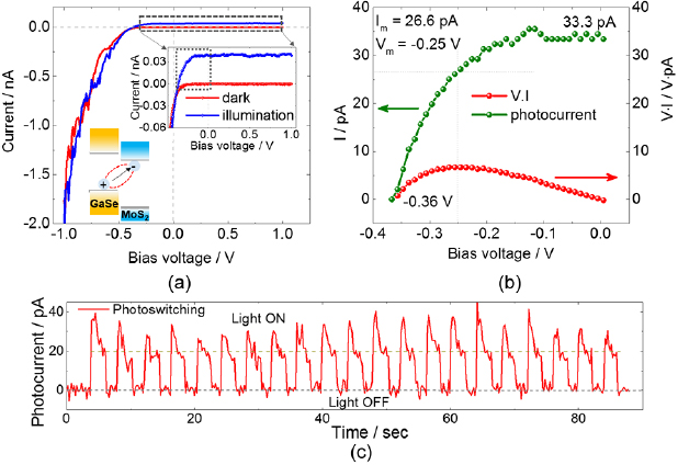
Figure 3. I–V curves of the heterostructure measured in dark and under illumination (a). The I–V curves within the dashed rectangular box are enlarged in the inset. Moreover, a sketch of the band alignment of the device is shown with interlayer exciton formation. I–V curve under illumination and corresponding V · I product of the dotted rectangular box (b). The short circuit current, open circuit voltage, and the fill factor of the device are determined to be (33 ± 1) pA, (−0.36 ± 0.1) V, and 55%. Demonstration of photoswitching at a bias voltage of 0 V (c). Dashed lines indicate the average photocurrents for light on and off. All photocurrent measurements were performed under 638 nm excitation.
Download figure:
Standard image High-resolution imageAnother very interesting observation of the photocurrent results as shown in figure 3 regards the excitation energy. The optical bandgap of bilayer MoS2 is 1.81 eV [68] and the exciton binding energy is about 0.43 eV [69]. Therefore, in order to dissociate excitons (created in MoS2) across the p-n interface one needs to illuminate with a photon energy of about 2.24 eV at least. On the other hand, the band gap of GaSe is 2 eV with an exciton binding energy of approximately 19 meV [70, 71]. Hence, to dissociate excitons generated in GaSe across the interface the minimum energy required is about 2 eV. In the present case, however, we can generate a photocurrent across the p-n interface using an excitation wavelength of 638 nm (equivalent to 1.94 eV). At comparable energies, density functional calculations have indicated spatially localized defect states associated with S vacancies [72, 73]. The conductivity in MoS2 in the very low carrier density regime was thus discussed in terms of a variable range hopping model [74], but the conductivity observed in the present investigation shows a homogeneous distribution of the photocurrent over the whole p-n interface. On the other hand, local defects such as metal vacancies or grain boundaries induce metallic states at the Fermi level even without illumination [75], which we did not observe in our measurement. We therefore conclude that local defects are not the dominating species involved in the photocurrent here. The observation of photocurrent can therefore be explained by the creation of interlayer excitons at the p-n interface as reported very recently in the literature [38, 39, 41]. To validate this hypothesis, we prepared another heterostructure of similar kind with two distinct interfaces and performed PL measurements. The results are displayed in figure 4. As shown in figure 4(a), MoS2 has two distinct interfaces; (1) with HOPG (interface I), and (2) with GaSe (interface II). In the first case, MoS2 creates a Schottky interface; whereas in the second case, a p-n junction is formed. The PL spectra of both interfaces in figure 4(b) resolve two excitonic peaks of MoS2 called A and B (1.88 eV, and 2 eV), while the PL emission of GaSe in the case of interface II is masked by the B peak of MoS2 (a comparative study of all PL spectra is shown in SI4). However, comparing the relative intensities of the PL peaks for both interfaces, one can see that the PL emission of MoS2 is quenched at the HOPG interface. This could be due to either a charging effect, a common phenomenon in MoS2 [76], or to quenching into the metallic HOPG substrate. Interestingly, in the case of interface II, a new broad feature around 1.48 eV is observed. This particular peak does not belong to either MoS2 or GaSe and is completely absent at interface I (HOPG|2ML-MoS2). This alien feature around 1.48 eV can, however, be formed by an e–h pair from adjacent layers of MoS2 and GaSe at the interface, known as interlayer exciton. The inset of figure 3(a) visualizes a likely mechanism of this type of exciton formation. Due to favourable band alignment at the interface, one can excite electrons from the valence band of GaSe to the conduction band of MoS2. The energy of the interlayer exciton peak suggests that it is possible to generate photocurrents with an excitation energy of 1.5 eV. To answer this question, we performed spatially resolved photocurrent mapping of the device shown in figure 2(b) using 785 nm (equivalent to 1.58 eV) excitation. The spatially resolved photocurrent maps are presented in figure 5. The AFM topography and the spatially resolved current map using CSAFM of the heterostructure in the dark at 0 V are depicted in figures 5(a) and (b). As expected, no current is observed in the CSAFM image scanned in the dark. However, under illumination with an excitation wavelength of 638 nm, the p-n junction shows a spatially distributed current map at the interface, which is in agreement with the results obtained in figure 3. Interestingly, the CSAFM images under illumination (figures 3(c) and (d)) resolve the heterointerface much better than the AFM topography in figure 3(a) since, photocurrents at p-n interface enhance the contrast of the heterointerface over dark GaSe region (no photocurrent). This is consistent with our interpretation, since the excitation energy is well below the band gap and exciton energies of GaSe amount to at least 2 eV in freshly cleaved samples [77]. The absence of the photocurrent at the HOPG|GaSe interface also confirms that the photocurrent generation solely depends on the GaSe|2ML-MoS2 interface properties. In addition, a photocurrent can be mapped at the p-n interface region under 785 nm excitation. This is a clear indication that we are accessing the interlayer excitons of 1.48 eV (838 nm) shown in figure 4(b). This further confirms the origin of photocurrents from interlayer excitons.
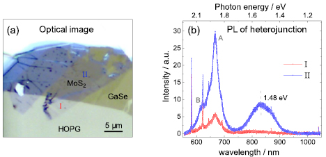
Figure 4. Optical image of the sample for PL measurements (a). Two distinct interfaces of MoS2 are created; (1) with HOPG (interface I), and (2) with GaSe (interface II). PL spectra of the two interfaces (b). Peaks A and B are PL emission from MoS2. A broad new feature around 1.48 eV is observed at the interface II and stems from interlayer excitons. The sharp lines are Raman features of HOPG.
Download figure:
Standard image High-resolution image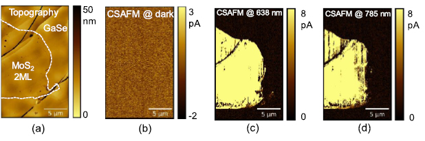
Figure 5. AFM topography of the heterostructure shown in figure 2(b) (a). A white dashed line is drawn at the boundary of the 2L-MoS2 to distinguish the heterostructure area. Spatially resolved current maps (CSAFM image) of the heterostructure in the dark (b), under 638 nm (c), and 785 nm (d) excitation. The CSAFM images were taken at 0 V. The observation of photocurrent at 785 nm excitation is a clear indication of interlayer excitons assisted photocurrent generation.
Download figure:
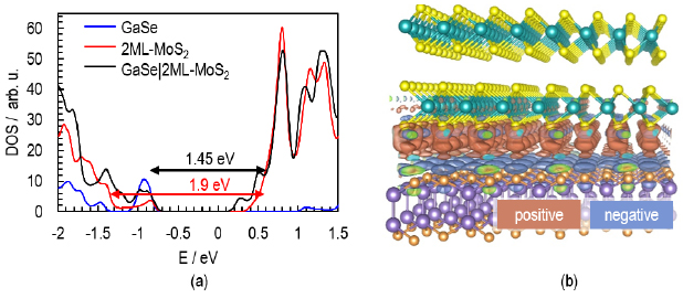
Standard image High-resolution imageIn order to get more insight into the interlayer exciton formation, density functional band structure calculations of the heterostructure were carried out. The generalized gradient approximation (GGA) was used to describe exchange and correlation. More details on the calculation are described in the supplementary information, SI5–6. The most important result is depicted in figure 6(a), where the density of states of the isolated layer systems (red and blue line) and their heterostructure (black line) are displayed. The arrows indicate the optically allowed electronic transitions (direct transitions/direct 'gap'). Indirect transitions from different k-points also contribute to the density of states and pretend some density inside the gap, which, however, cannot be probed optically. The hybridization of the electronic states between the different layers is small and the underlying selection of the transitions and the according band structures are discussed in detail in the supporting information. Figure 6(a) shows that for the combined system (black line) additional states appear in the valence band region. Such states are not observed in isolated MoS2 and clearly stem from GaSe. The electronic transition between these states from the valence band of GaSe to the conduction band of MoS2 are optically allowed and contribute to the PL. Further, the energy differences for the direct transitions between valence and conduction band agree very well with the observed features: the A-exciton of MoS2 can be found at about 1.9 eV (1.88 eV in the experiment) and the interlayer transition at about 1.45 eV (1.48 eV in the experiment). It should be noted that the selection rules for the optical transitions in k-space depend on the rotation angle between the two layers, whereas the density of states is nearly independent of the rotation angle (besides differences due to different hybridization patterns—which is, however, shown to be small). The rotation of the layers with respect to each other in the experiment is not specified, and may vary from device to device. As the bands that contribute to the interlayer exciton may depend on the rotation angle (according to the selection rules in k-space) and the rotation in the experiment cannot be controlled, many different bands in about the same energy range may contribute to the interlayer exciton. This could be the reason why the signature in figure 4(b) is extremely broad as indicated already in the density of states. More details of the theoretical analysis can be found in the supporting information. Additionally, the partial oxidation of the GaSe surface discussed above may also change the interlayer excitons slightly and may add to the broadening of the interlayer exciton peak.
Figure 6. (a) DFT band structure of the isolated layers GaSe (blue line) and bilayer MoS2 (red line) and the interacting layers GaSe|2ML-MoS2 (black line). The direct band transitions of the respective layers are indicated by arrows of the corresponding color: MoS2 (1.9 eV, red) and GaSe|2ML-MoS2 (black). The transitions are selected ones according to the band structure calculations provided in the supporting information SI5 and SI6. (b) Charge density difference plot of the bilayer MoS2 on the GaSe: negative charge (blue) is transferred from MoS2 to GaSe and leads to a p-doping of MoS2.
Download figure:
Standard image High-resolution image
From a methodological point of view, this agreement of the DFT data with the experiment is, to some extent, accidental: principally, DFT is not able to accurately predict optical transitions. For a more rigorous treatment, quasi particle excitations and exciton formation should be taken into account—which is, however, extremely challenging for this setup, as the selection rules depend on the orientation angle between the layers. However, as quasi particle corrections and exciton formation counter correct each other (approximately), the DFT transitions are sufficient in the present case to demonstrate the concept of the interlayer exciton formation and support the experimental finding.
Figure 6(b) depicts the charge density difference when the bilayer MoS2 interacts with the GaSe monolayer: negative charge (blue) is transferred from bilayer MoS2 to the GaSe substrate and leads to its p-doping (as expected for a p-n interface formation with a type II band alignment). As the density of states in figure 6(a) is hardly perturbed, the electronic structure of each layer remains almost the same; a more detailed k-resolved confirmation of this picture is given in the supplementary information. Thus, the interface-related polarization together with a partial transfer of hole density from GaSe to MoS2 is the underlying mechanism, which leads to both the doping effect and the additional interlayer excitons as the most important features of the bilayer GaSe|MoS2 hybrid system regarding electronic applications.
Conclusion
We demonstrated diode rectification behaviour of a 2D p-n interface made of few layer GaSe and bilayer MoS2. Interestingly, the p-n interface gives rise to photocurrent under below bandgap excitation. The phenomenon is explained by interlayer excitons which is further proved by PL measurement at the interface showing a feature around 1.48 eV, which corresponds to interlayer excitons. Photocurrent mapping at the interface under illumination with a wave length of 785 nm excitation (equivalent to 1.58 eV) resolves the p-n interface and confirms the interlayer exciton dissociation. Finally, DFT calculations are introduced to validate the experimental results and confirm the interlayer exciton formation at the p-n interface. To the best of our knowledge, this is the first experimental demonstration of the interlayer excitons in photovoltaic applications of vdW heterojunctions. Our findings not only further the basic understanding of this new type of vdW heterostructures but also shed light on the next generations of 2D material based optoelectronic devices.
Acknowledgment
We would like to thank DFG Research Unit FOR 1497, DFG Research Unit FOR 1713, and the DFG Cluster of Excellence CFAED (Center for Advancing Electronics Dresden) for supporting the research work. SG and CW acknowledge funding by the Helmholtz Initiative and Networking Funds via project W2/W3-026.