
Abstract
Using atomistic quantum simulation based on a tight binding model, we have investigated the transport characteristics of graphene nanomesh-based devices and evaluated the possibilities of observing negative differential conductance. It is shown that by taking advantage of bandgap opening in the graphene nanomesh lattice, a strong negative differential conductance effect can be achieved at room temperature in pn junctions and n-doped structures. Remarkably, the effect is improved very significantly (with a peak-to-valley current ratio of a few hundred) and appears to be weakly sensitive to the transition length in graphene nanomesh pn hetero-junctions when inserting a pristine (gapless) graphene section in the transition region between n and p zones. The study therefore suggests new design strategies for graphene electronic devices which may offer strong advantages in terms of performance and processing over the devices studied previously.
Export citation and abstract BibTeX RIS
1. Introduction
Graphene nanostructures have emerged as natural candidates for developing 'beyond CMOS' nanoelectronics [1–4]. In particular, thanks to its high charge carrier mobility [5], graphene is expected to emerge as an excellent material for radiofrequency (RF) electronic applications [2–4]. In various devices based on conventional semiconductors, the effect of negative differential conductance (NDC) has been exploited for high frequency applications [6]. Hence, this effect has been investigated in several graphene structures (see, e.g., [7–13]). However, due to the lack of bandgap in 2D graphene systems [7–10] or to the influence of edge defects in narrow graphene nanoribbons (GNR) [12, 13], it was shown that the NDC effect is generally weak in such structures.
Recently, we have demonstrated that a strong NDC effect can be achieved in graphene pn junctions [14], and especially in GNR hetero-structures [15], with a peak-to-valley current ratio (PVR) of at least a few hundred at room temperature. To obtain such a strong effect, a large energy bandgap in the graphene channel is essential. This may be realized by growing the graphene sheet on a SiC substrate [16] or by using armchair GNRs [17]. Indeed, an increase in the bandgap strongly reduces the valley current and may result in an increase in the PVR of NDC [14]. However, a large bandgap also results in the appearance of evanescent states in the transition region between p-doped and n-doped zones, which reduces the peak current. This feature limits the operation of the junction when the transition length is large and difficult to control accurately. In [15], by taking advantage of the possibilities of bandgap engineering in armchair GNRs, we demonstrated that the NDC effect can be improved significantly in specific GNR pn hetero-junctions wherein the bandgap is large in two junction sides while it is small in the transition region. This improvement comes from the fact that due to the small or even vanishing bandgap in the transition region, the interband tunneling is enhanced in the peak current regime, while the valley current remains small since it is limited by the bandgap width in the two highly doped sides of the junction. However, though it was shown to provide a very strong NDC effect, this GNR design still raises a technological issue regarding the precise control of the ribbon shape and edges.
Experimentalists have recently reported the fabrication of a new graphene nanostructure called a graphene nanomesh (GNM) [18–21] in which the size of nanoholes and the distance between them can be controlled down to the sub-10 nm scale. Various techniques have been developed to produce such GNM lattices, such as block copolymer lithography [18, 19], nanosphere lithography [20], and nanoimprint lithography [21]. This type of nanostructuring may open up a bandgap in large sheets of graphene to create semiconducting thin films. Moreover, it was demonstrated that GNM-based transistors can support driving currents nearly 100 times greater than individual GNR devices, with a comparable on–off ratio [18]. On this basis, the GNM lattices with variable periodicity and neck width are expected to offer various possibilities of bandgap engineering, and therefore of graphene electronic applications.
These considerations suggested that we examine in this work the possibility of using GNM lattices to design effective NDC devices. In comparison with the devices based on graphene epitaxially grown on a SiC substrate [14], GNM devices may offer the advantage of various possibilities of bandgap engineering while providing higher driving current than the GNR structures [15]. Additionally, for practical use, by means of the experimental techniques mentioned above GNM lattices should be much easier to produce and handle than GNRs.
2. Model and calculation
In the graphene honeycomb lattice of carbon atoms, the charge transport can be described well by a simple nearest-neighbor tight binding model [22]. The Hamiltonian of conduction electrons in graphene hence reads

where Un is the on-site/potential energy that can be modulated by the external voltage, Cn ( ) is the operator which annihilates (creates) an electron on the nth site of the graphene lattice, and the sum in 〈n,m〉 is restricted to the nearest-neighbor atoms with a hopping energy t ≈ 2.7 eV [23]. To conveniently study the charge states in GNM lattices, the structure may be split into elementary cells as shown in figure 1(a). The Hamiltonian (1) can therefore be expressed in the following form:

where Hp,q is the Hamiltonian of cell {p,q}, Hp,q→q±1 denotes the coupling of cell {p,q} to cell {p,q ± 1}, and Hp→p±1,q the coupling of cell {p,q} to cell {p ± 1,q}.
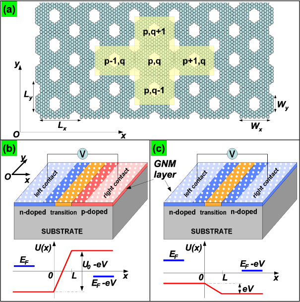
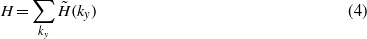
Figure 1. (a) Atomistic lattice of a GNM sheet and ((b), (c)) sketch of GNM devices considered in this work together with their potential profile (red solid line): (b) pn junction and (c) n-doped structure. U0 in (b) is the potential barrier at zero bias which results from the difference in doping levels between the two sides of the pn junction [8, 14, 15, 29]. EF (EF − eV) indicates the Fermi level in the left (right) contact at finite bias.
Download figure:
Standard imageIn the simulated devices, we assume the lateral size (along the OY direction) of the GNM sheet to be much larger than the length (along the OX direction) of the active region between the two contacts (seen in figures 1(b) and (c)), e.g. about a few tens of nanometers. Therefore, the potential energy U in equation (1) can be modeled as a function of x only. This assumption neglects the influence of graphene edges and lateral confinement effects which are important for narrow GNR channels. On this basis, the GNM channel is considered as an infinite sheet and the translational symmetry of the crystal lattice can be applied along the OY direction, i.e. similar to the 2D graphene systems studied in [10]. Hence, we can Fourier transform the operators in equation (2) as follows:

where the indices {n,p,q} denote the nth site in the cell {p,q}, Lx,y indicates the size of an elementary cell of the GNM lattice (see figure 1(a)), and Mcell, assumed to be very large, is the number of periodic structures along the OY direction. The Hamiltonian (2) is finally rewritten in the following decoupled form:

In this form, since the terms  are obtained by Fourier transform of the operators Hp→p±1,q which describe only the coupling between the cells of the same index q, they are ky-independent. In contrast, the term
  determined from the Fourier transform of the first three operators in equation (2) is ky-dependent.
From the Hamiltonian (4), the non-equilibrium Green's function formalism [22, 24–26] can be easily applied to study the charge transport in GNM structures. With the assumption that left and right contacts are semi-infinite along the transport direction OX, the problem of device-to-contact coupling is solved as a boundary condition [24], which is encoded in terms of the so-called self-energy. The device retarded Green's function for a given momentum ky is then defined as

where ΣL(R) is the self-energy describing the device-to-left (-right) contact coupling. In our simulation, this equation is solved using the recursive Green's function algorithms as in [22, 25, 26]. The transmission probability needed to define the current is calculated as T(E,ky) = Tr[ΓLGΓRG†], where  is the transfer rate at the left (right) contact. The current is then computed using the Landauer formula:
where fL(R)(E) = 1/[1 + exp((E − EFL(R))/kbT)] is the left (right) Fermi distribution function with the Fermi level (chemical potential) EFL(R), and the integral on ky is performed in the first Brillouin zone.
The above formalism is used to investigate the transport characteristics of the GNM devices schematized in figures 1(b) and (c) with the GNM atomistic lattice as shown in figure 1(a). The doped graphene regions are assumed to be possibly generated by using electrostatic doping [27–29] or by chemical doping [30, 31]. Between the p-doped and n-doped zones, there is a transition region wherein the charge density changes monotonically from n-type to p-type. The potential profile U(x) is hence modeled as in figures 1(b) and (c). This model of a pn junction is similar to that studied in [8, 14, 15, 29]. Throughout this work, the ballistic current is investigated at room temperature.
3. Results and discussion
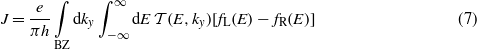
We first present in figure 2(a) a picture of the electronic band structures of a GNM lattice obtained by solving the Hamiltonian (2). Note that with the aim of demonstrating the typical transport characteristics of GNM devices, throughout this work the results presented were obtained for lattices based on a particular nanohole shape wherein 24 carbon atoms are removed as shown in figure 1(a). The most important property of GNM lattices is the energy bandgap opening that makes them semiconducting while 2D pristine graphene sheets are semi-metallic. This property has been predicted theoretically using a tight binding model and/or the density functional theory [32–34], and has also been demonstrated experimentally [18–21]. It was shown that the electronic structure of GNM lattices depends strongly on the density (lattice periodicity), size and shape of nanoholes. More importantly, it has been shown that a GNM lattice may be seen as a multiple GNR network. Therefore, its bandgap was demonstrated to originate from the finite size effect of these effective nanoribbons and to be inversely proportional to the GNR width [21, 32, 34]. This important feature is illustrated in figure 2. Indeed, it shows that a finite bandgap Eg (i) appears around the zero energy point (see figure 2(a)) and (ii) increases with decreasing Wx,y (see figure 2(b)), where Wx,y are the GNR widths along the OX and OY directions, respectively (see figure 1(a)). Moreover, another significant characteristic of the GNM lattice is also observed in figure 2(a), i.e. the existence of mini-bands and mini-gaps Emini−gap. Such a feature appears very frequently in many structures with different nanohole sizes and shapes, e.g. [32–34]. The band structure of GNM lattices hence offers various possibilities for a controllable energy bandgap, which opens many opportunities for graphene electronic applications such as the pioneering device named GNM–FET [18, 21].
Figure 2. (a) Energy band structure of a GNM lattice as in figure 1(a) and (b) evolution of its bandgap Eg as a function of 1/Wx for different Wy.
Download figure:
Standard imageTaking advantage of the bandgap engineering discussed above, we now investigate the use of GNM lattices to design effective NDC devices.
3.1. GNM pn junctions
As suggested by [14], we now study the pn junction (see figure 1(b)), a building block of the well-known tunnel diode [35]. In such a structure, the interband tunneling of charge carriers from filled electron states (in the conduction band) in the n-side to empty hole states (in the valence band) in the p-side results in a high peak current at low bias. The valley current (NDC effect) occurs at high bias when the filled states in the n-side find a reduced number of empty states available for tunneling in the p-side. The latter feature can be observed clearly in the case of a large bandgap in the channel material [14, 35]. Actually, the GNM lattices with the electronic structure shown above meet such a condition well. In figure 3, we present a schematic band diagram (a) and the I–V characteristics for different transition lengths L (b) of the pn junction using the GNM lattice studied in figure 2(a). In this band diagram, the thermionic regions correspond to the energy ranges above the potential barriers (for electrons and holes) in which the contribution to the total current may be significant at high temperature. Though small in normal operation, the thermionic current must be considered carefully since it can result in an increase in the total current in the valley regime. Due to a finite bandgap (Eg ≈ 0.27 eV, see in figure 2(a)), a strong NDC effect can be observed in the considered device (see figure 3(b)). However, as discussed for graphene-on-SiC structures in [14] and schematically described in the diagram of figure 3(a), the interband tunneling through the pn junction is strongly influenced by evanescent states (due to the channel bandgap) around the neutral points in the transition region, i.e. around the red line in figure 3(a) which corresponds to the potential profile in the middle of the bandgap. Therefore, as similarly demonstrated by figure 2 of [14], this tunneling is reduced when increasing the length L and/or the bandgap Eg. Such a feature essentially explains the strong reduction in the peak current and the PVR with increasing L observed in figure 3(b). In spite of this effect, the PVR obtained here is still high (i.e. ∼320, 90, and 30 for L ≃ 5.5 nm, 11.1 nm, and 22.1 nm, respectively) in comparison with that reported (≤16) in conventional tunnel diodes (see [36] and references therein).
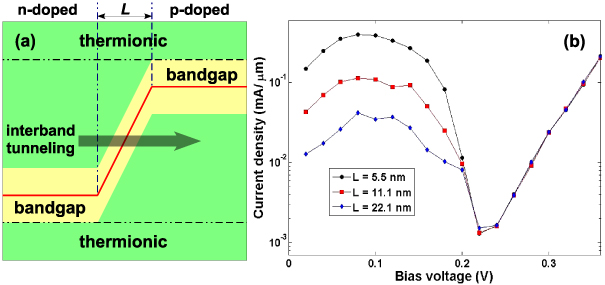
Figure 3. (a) Schematic band diagram and (b) semilog plots of the I–V characteristic of simple GNM pn junctions obtained for different transition lengths. The red solid line in (a) indicates the potential profile of the device at the neutral point, i.e. in the middle of the bandgap. It is modeled as in figure 1(b). The GNM lattice is as that studied in figure 2(a) and the potential barrier U0 = 0.5 eV.
Download figure:
Standard image3.2. n-Doped GNM structures
We next propose to design another NDC device where instead of different doping levels as in the pn junction, the same n-doped GNM sections are used in both sides of the device as schematized in figure 1(c). In this device, the normal transmission within a miniband leads to a high peak current at low bias. Due to the finite mini-gap, when the applied voltage is high enough, the filled states in the left side find a reduced number of empty states in the right side as schematically described in the diagram of figure 4(a). Therefore, the transmission probability/the current decreases when increasing the bias. Indeed, this idea is demonstrated by the I–V curves for different Fermi levels EF shown in figure 4(b). On the one hand, the NDC effect is observed in all cases of different EF. On the other hand, both the peak and valley currents are reduced when decreasing EF. The study therefore shows that the strongest NDC effect is achieved when EF ≈ Ec + Emini−gap, where Ec and Emini−gap are the bottom of the conduction band and the width of the mini-gap, respectively. For instance, the largest PVR observed in figure 4(b) is about 5.8 for EF = 0.25 eV, while Ec ≈ 0.135 eV and Emini−gap ≈ 0.115 eV. Note that though the obtained NDC effect (due to the small mini-gap, i.e. Emini−gap < Eg) is not as strong as in the GNM pn structures, the advantages of this design are (i) the high current density (due to normal transmission instead of the interband tunneling) and (ii) the fact that the device operation is not affected by the change in the transition length L as in the pn junctions discussed above.

Figure 4. (a) Schematic band diagram and (b) I–V characteristics of an n-doped GNM structure plotted for different Fermi levels EF. The device is modeled as in figure 1(c), the GNM lattice as studied in figure 2(a) is used, and the length L = 11.1 nm.
Download figure:
Standard image3.3. GNM/pristine graphene/GNM pn hetero-junctions
As suggested by [15], to reduce the sensitivity of the peak current and the PVR to the transition length in GNM pn junctions as discussed in section 3.1, we propose to use GNM/pristine graphene/GNM hetero-structures wherein the bandgap (of pristine graphene) in the transition region is zero. The schematic band diagram and the I–V characteristics for different L of such pn hetero-junctions are shown in figure 5. The idea is explained as follows. Due to the gapless character of pristine graphene, while the evanescent states around the neutral points in the transition region were observed clearly in the normal gapped graphene structures, as schematically drawn in the diagram of figure 3(a) or as similarly shown in the local density of states (LDOS) of GNR structure plotted in figure 3(a) of [15], they do not appear in the proposed pn hetero-junctions, as schematically illustrated in the diagram of figure 5(a) or as similarly shown in the LDOS displayed in figure 3(b) of [15]. Hence, while the valley current controlled by the large bandgap in both junction sides is maintained at a low value, the current peak is enhanced significantly and becomes much less sensitive to L (see figure 5(b)) in comparison with that in the normal GNM pn junctions (figure 3(b)). As a consequence, a PVR of about a few hundred can be achieved even for large L, e.g. L = 44.3 nm here, which cannot be obtained in normal junctions. However, though the bandgap is zero in the transition region, figure 5(b) (see the inset) shows that the peak current is still slightly reduced with increasing L. It is basically different from the armchair GNR hetero-junctions [15] where the results are independent of L if the bandgap is actually zero in the transition region. This behavior can be understood as follows. It should be kept in mind that the charge transport through a pristine graphene sheet is governed by its electronic structure around the Dirac (K-) point [37], where the energy dispersion obtained from the tight binding model (1) tends to the form  (e.g. see [1]) with q = k − K and vF ≈ 106 ms−1. Hence, there exists an energy gap
  which is actually zero for qy = 0 but is finite for other momenta in the pristine graphene section. As a consequence, though the magnitude of the transmission probability is unchanged when increasing L for qy = 0 (
 ), as illustrated in figure 5(c), it is slightly reduced for other modes (finite
  ), as seen in figure 5(d). This feature and the fact that the current here results from the contribution of many momentum modes ky (see equation (7)) explain well the small dependence of the peak current/the PVR on L observed in figure 5(b).

Figure 5. (a) Schematic band diagram and (b) semilog plots of the I–V characteristic of GNM/pristine graphene/GNM pn junctions obtained for different transition lengths L. The red solid line in (a) indicates the potential profile (neutral points) of the device, which is modeled similarly to that in figure 1(b). The inset in (b) shows the I–V curves plotted on a linear scale. Parts (c) and (d) show the dependence of the transmission probability on L for different ky corresponding to the ky-dependent energy gaps  and 98 meV (see discussions in the text). The GNM lattice is like that studied in figure 2(a), the longitudinal size of pristine graphene of 60 nm ( > L) is used, and U0 = 0.5 eV.
Download figure:
Standard image4. Conclusion
Using the non-equilibrium Green's function technique within a tight binding model, we have investigated and evaluated the design of some NDC devices based on GNM lattices. Due to quantum confinement in their GNR-like network, the GNM lattices offer various possibilities for a controllable energy bandgap, e.g. when changing the nanohole size and spacing. On this basis, we have demonstrated that a strong NDC effect can be achieved at room temperature in GNM pn junctions and in n-doped GNM structures. While a high PVR of NDC can be obtained in the former structures at the price of strong sensitivity to the transition length L, the peak current is high and is not affected when changing L in the latter structures. Remarkably, in GNM/pristine graphene/GNM pn hetero-junctions both a high peak current and a very high PVR (a few hundred) can be observed and are proved to be weakly sensitive to the transition length. We hope that this study will stimulate further investigations of the possible applications of GNM lattices with the benefit of bandgap engineering which is no longer restricted to narrow GNRs but may now be extended to large sheets of graphene.
Acknowledgments
This work was partially supported by the French ANR through the projects NANOSIM-GRAPHENE (ANR-09-NANO-016) and MIGRAQUEL (ANR-10-BLAN-0304). The authors would like to thank Mairbek Chshiev for useful discussions. One of the authors (VHN) acknowledges the Vietnam National Foundation for Science and Technology Development (NAFOSTED) for financial support under project no. 103.02-2010.33 and thanks Huy Viet Nguyen for fruitful discussions on computational techniques.