
Abstract
We propose and demonstrate strongly enhancing electric field and Raman scattering with a large tolerance to the light incident angle and polarization by using x-shaped quasi-3D plasmonic nanostructure arrays (X-Q3D-PNAs). The finite-difference time-domain simulations were used to study the reflectance spectra and electric field profiles of X-Q3D-PNAs. Results show that both surface plasmon polaritons and localized surface plasmon polaritons (LSPPs) can be generated at the metal/dielectric interfaces of the top gold thin film with square grating x-shaped nanoholes. The resonance of the LSPPs generated at the gold islands formed between x-shaped nanoholes at the top gold thin film greatly enhance the electric fields at the tips of the cross-sectors of the x-shaped nanoholes. Both plasmon resonances and electric field enhancements are affected by the structural dimensions. The strong electric field enhancement and the large tolerance to the laser polarization were demonstrated by surface-enhanced Raman scattering experiments. This unique plasmonic property of X-Q3D-PNAs could be attractive for photovoltaics and biosensing applications.
Export citation and abstract BibTeX RIS
1. Introduction
Plasmonic nanostructures containing subwavelength metallic nanoholes and nanodisks can greatly enhance the local electric fields in the vicinity of metallic nanostructures due to the localized surface plasmon resonances (LSPRs) arising from the coherent oscillation of free conduction electrons of metal excited by the incident light [1]. This fascinating optical property has led to a variety of applications ranging from manipulating [2] and enhancing light transmission [3–7], absorption [8–11], and emission [12–14] for photonic and optoelectronic devices to enhancing vibrational spectroscopy for sensitive chemical and biological detection and sensing [15–19]. The plasmonic and optical properties of plasmonic nanostructures strongly depend on the size, shape, and spatial arrangement of the subwavelength constituents, and the dielectric media [20–24].
Plasmonic nanostructures made out of quasi-3D plasmonic nanostructure arrays (Q3D-PNAs) have simple structures and are easy to fabricate, and they also exhibit rich plasmonic and optical properties. Composed of a gold thin film with subwavelength nanoholes on the top and gold nanodisks at the bottom of the nanowells, Q3D-PNAs can be fabricated by one-step electron beam lithography (EBL) [25–27] or nanoimprinting [28, 29] followed by metallization. The electromagnetic energy is confined to nanoscale volumes due to the interplay of different plasmonic elements and surrounding dielectric materials. Both propagating surface plasmon polaritons (SPPs) and localized surface plasmon polaritons (LSPPs) are generated at the top gold film with a nanohole array. The resonance of SPPs can be described using the Bloch wave SPP (BW-SPP) model and is sensitive to the lattice periodicity and surrounding dielectric materials [27, 28, 30]. The LSPPs can be generated at both the top gold thin film with periodically arranged nanoholes and bottom gold nanodisks. The upper surface of the gold nanodisks at the bottom and the bottom surfaces of the nanoholes on the top create a Fabry–Pérot (FP) resonant nanocavity [27]. In addition, both the dielectric material (e.g. photoresist) that separates the top and bottom gold layers and the materials of the substrates on which Q3D plasmonic nanostructures are fabricated influence the overall plasmonic and optical properties [31]. It was reported that the light transmission and surface-enhanced Raman scattering (SERS) effects significantly depend on the depth of the FP resonant nanocavity [30, 31]. Investigations of the circular Q3D-PNAs showed that the intensity and the location of the maximum enhanced local electric field can be tuned to either the top gold nanoholes or bottom gold nanodisks by varying the diameter of the nanoholes [32] or the depth of the FP nanocavities [31]. This unique plasmonic property has been applied for the optimal detection of small molecules and large microorganisms using SERS [32]. It has also been reported that the coupled LSPR peak [28] and the FP resonance peak [27] are highly sensitive to the refractive index (RI) change and their application for biosensing has been exploited.
While all the previous investigations of Q3D-PNAs have been focused on the circular-shaped nanostructures, it is known that nanostructures with vertices such as triangle [33, 34] and bow-tie [35, 36] ones can confine the electromagnetic energy in the tips, resulting in strong local electric fields at the fixed locations. In this work, we demonstrate that x-shaped Q3D-PNAs (X-Q3D-PNAs) can efficiently confine the electromagnetic energy to the tips of the cross-sectors of the x-shaped nanoholes with a large tolerance to the light incident angle and polarization. The finite-difference time-domain (FDTD) simulations were first conducted to investigate the reflectance spectra and electric field profiles as a consequence of the interplay of different plasmonic elements as well as their dependence on the structural dimensions and the light incident angle and polarization. The X-Q3D-PNAs were then fabricated via EBL and the reflectance spectra were measured experimentally. Finally, the strong energy confinement was verified by SERS experiments and the large tolerance to the variation of the laser polarization was also demonstrated.
2. Experiments and methods
2.1. FDTD simulations
The FDTD method4 was used to calculate the reflectance spectra and electric field profiles of X-Q3D-PNAs. Figure 1(a) depicts the 3D structure and 2D top view of an X-Q3D-PNA. The simulations were conducted using a single x-shaped Q3D nanostructure as a unit cell with an infinite periodic Bloch boundary condition. A continuous wavelength (cw) plane wave light source was placed 450 nm above the top gold/air interface. One monitor at 50 nm above the light source was used to collect the reflectance spectrum from the X-Q3D-PNA. The other two monitors were placed at the top gold/air interface and the cross-sectional x–z plane at the center of the x-shape to obtain the near-field electric field profiles. The mesh size was set as 3 nm in three dimensions throughout the simulation unit cell. The wavelength-dependent refractive indices of gold and silicon in the simulation wavelength range were adapted from those provided in the software database. For PMMA, the wavelength-dependent refractive index was obtained from the ellipsometry measurements on the PMMA thin films spun on silicon substrates. The X-Q3D-PNA is considered to be exposed to air.
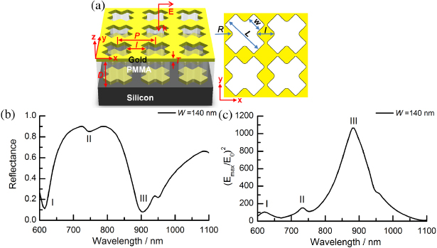
Figure 1. (a) A 3D illustration and a 2D top view of the X-Q3D-PNA on a silicon substrate. The key parameters varied in the FDTD simulations are labeled. (b) The FDTD simulated reflectance spectrum of an X-Q3D-PNA with the parameters of lattice periodicity P = 520 nm; separation depth D = 400 nm; length and width of the x-shape L = 420 nm and w = 140 nm; curvature of the tips of the cross-sectors of the x-shape R = 40 nm; and thickness of the gold layer T = 50 nm. The light is illuminated normally from the gold side with the polarization along the x-direction. (c) The electric field enhancement in terms of |Emax/E0|2 as a function of the wavelength, where the Emax are the maximum electric fields at the top gold/air interface at each wavelength and E0 (1 V m−1) is the electric field of the incident light.
Download figure:
Standard image2.2. Fabrication of X-Q3D-PNAs
A clean silicon wafer was spin coated with 400 nm PMMA photoresist (Microchem, 950 K), baked at 180 °C for 90 s, and then cut into 10 mm × 10 mm square chips. The thickness of PMMA was measured by ellipsometry. EBL was performed using an FEI Sirion scanning electron microscope (SEM) equipped with a Nabity nanopattern generation system (NPGS). A fine electron beam (spot size 1) with the line dose of 0.32 nC cm−1 and a small beam center-to-center distance of 10 nm were used in order to obtain x-shapes that were better written. The total written area was 150 μm × 150 μm. The nanohole pattern was generated after development in 3:1 isopropanol:methyl isobutyl ketone (IPA:MIBK) PMMA developer for 70 s followed by an IPA rinse and a N2 blow-dry. The X-Q3D-PNA was formed by depositing a 50 nm gold onto the nanohole array substrate in a thermo-evaporator (Edward, auto 306) at the deposition rate of 0.1 nm s−1 under the background pressure of 2 × 10⁻⁶ mbar.
2.3. Optical reflectance spectra measurements
The reflectance spectra were measured via a laboratory setup. White light from a halogen lamp (Ocean optics, HL-2000) was guided via an optical fiber and then collimated and polarized along the x-direction defined in figure 1(a). The light was reflected to 90° by a beamsplitter to illuminate an X-Q3D-PNA at normal incidence. The reflected light from the array was collected through an objective (4 × , 0.1 NA, Nikon) into an optical fiber connected to a spectrometer (Ocean optics, S2000). All reflectance spectra of X-Q3D-PNAs were normalized to the spectrum collected from a flat gold surface.
2.4. SERS measurements
A fresh gold coated chip was rinsed with deionized (DI) water and cleaned in a UV ozone cleaner for 20 min before being immersed into 3 mM 4-mercaptopyridine (4-MP, Sigma) solution for 3 h to form a self-assembled monolayer (SAM). The chip was rinsed with DI water intensively to ensure that only one monolayer of 4-MP molecules was formed on the gold surface. The SERS measurements were conducted using a Renishaw InVia Raman spectrometer connected to a Leica DMLM upright optical microscope. A 785 nm diode laser was used to excite the Raman scattering and the laser power after a 10 × objective was measured using a handheld power meter (Edmund Optics). The SERS spectra in different polarization directions were acquired by mounting the chip on a small rotation stage.
3. Results and discussion
3.1. FDTD simulated reflectance spectra and electric field profiles
Figure 1(a) depicts the structure of an X-Q3D-PNA fabricated via one-step EBL followed by gold deposition. The structure consists of two plasmonic layers: a gold thin film with a 2D array of x-shaped nanoholes on the top and a 2D array of x-shaped gold nanodisks at the bottom. They are physically separated by a layer of the dielectric material PMMA and air cavities above gold nanodisks. The top gold thin film has a unique structure. Stripes of continuous gold films exist between rows (x-direction) and columns (y-direction) of x-shaped nanoholes, which support propagating SPPs. Gold islands with tips on both sides are formed between x-shaped nanoholes in the same row and column. Because these islands are isolated by the nanoholes, LSPPs can be generated on these islands. But since these islands are connected to the continuous strips of gold thin films, they also can support SPPs. The key parameters that influence the plasmonic properties of X-Q3D-PNA are labeled in figure 1(a), including the length (L), width (W), and curvature (R) of the x-shaped nanohole, the periodicity (P) of the square grating array, the depth (D) of the cavity, and the thickness (T) of the gold film. The length (I) of the gold island is also indicated in figure 1(a), which can be calculated by using the formula  when the curvature (R) is ignored.
Figure 1(b) shows the FDTD simulated reflectance spectrum from an X-Q3D-PNA illuminated by normally incident light with the polarization parallel to the x-direction. Three obvious dips at ∼610, ∼730, and ∼900 nm, marked I, II, and III, respectively, and one shoulder at ∼950 nm are observed in the reflectance spectrum in the range of 600–1100 nm. The dips in the reflectance spectrum are caused by different plasmonic modes generated upon the light illumination of the X-Q3D-PNA. The electric field enhancement was estimated by using the relationship of the square of the maximum local electric field at the top gold/air interface with respect to the incident electric field (|Emax/E0|2). The plot of |Emax/E0|2 versus wavelength in figure 1(c) clearly shows that the peaks in the electric field enhancement spectrum correspond to the dips in the reflectance spectrum. Note that the calculated local electric fields depend on the mesh size used in the FDTD simulations because of the exponential decay of the electric field from the metal surface. A simulation was conducted by using the same mesh size in the x- and y-directions but reducing the mesh size to 0.5 nm in the z-direction for the same X-Q3D-PNA. The results show that the reflectance spectrum is not affected, but the value of electric field enhancement (|Emax/E0|2) increases about 3.5-fold from 1064 to 4032 for mode III (figure S1 in the supporting information available at stacks.iop.org/Nano/23/405201/mmedia). Because the features of the fundamental interactions of photons and an X-Q3D-PNA are not influenced by the mesh size, the mesh size of 3 nm in three directions throughout the unit cell was used in all the FDTD simulations.
The electric field profiles at the top gold/air interface (Column A) and the cross-sectional x–z plane (Column C) at the wavelengths corresponding to the dips (modes) I, II, and III in figure 1(b) are plotted in figure 2. The electric charge profiles overlaid with the Poynting vector maps at these two planes are shown in Columns B and D in figure 2. Mode I generates weak electric field enhancements at the four ends of the x-shaped nanohole and at the gold/PMMA interface due to counter-propagating SPPs at both gold/air and gold/PMMA interfaces as indicated by the Poynting vectors. Opposite charges resulted from the counter-propagating SPPs. Mode II generates weak electric field enhancements at the four ends and at the cross-sectors of the x-shaped nanohole. Poynting vectors clearly show that the energy flux flows along the edges of the four ends of the x-shaped nanohole and confines the energy at the cross-sectors of the x-shaped nanohole, which is also due to counter-propagating SPPs. Poynting vectors in the cross-sectional x–z plane show the coupling of SPPs between the gold/air and gold/PMMA interfaces, resulting in an enhancement of the electric field at the edge of the cross-sectors of the x-shaped nanohole. In contrast to modes I and II, mode III induces very strong electric fields at the tips of the cross-sectors of the x-shaped nanohole along the x-direction and almost no enhancement at the four ends. Poynting vectors directly point towards the tips of the cross-sectors of the x-shaped nanohole, indicating LSPPs generated at the gold islands between x-shaped nanoholes in the same row. The cross-sectional electric field profile shows strong electric field enhancement at the edges of the cross-sectors of the x-shaped nanohole, which resulted from the coupling of LSPRs at the gold/air and gold/PMMA interfaces of the gold islands as indicated by the Poynting vectors. The shoulder at ∼950 nm in the reflectance spectrum could be due to the LSPPs at the gold nanodisk at the bottom, which will be discussed in section 3.2.
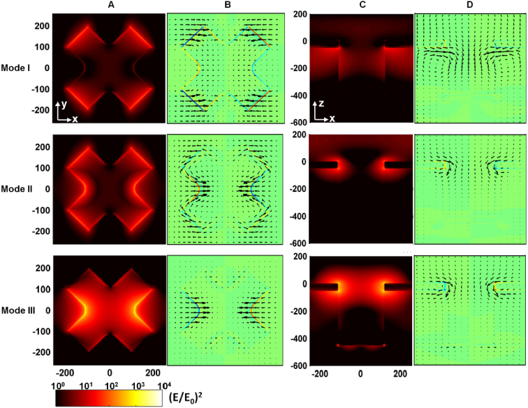
Figure 2. The electric field profiles and the maps of the electric charge distribution and Poynting vector corresponding to the dips (modes) I, II, and III of the reflectance spectrum shown in figure 1(b). The electric field profiles at the top gold/air interface and at the cross-sectional x–z plane at the center of x-shaped cavity are shown in Columns A and C, respectively. The maps of charge distribution overlaid with the maps of the Poynting vector at the top gold/air interface and at the cross-sectional x–z plane at the center of the x-shaped cavity are shown in Columns B and D, respectively.
Download figure:
Standard image3.2. The dependence of the plasmonic properties on the structural dimensions
Poynting vectors in figure 2 indicate that the dips I and II in the reflectance spectrum of the X-Q3D-PNA are mainly due to the SPP Bloch wave modes along the gold/air and gold/PMMA interfaces of the top gold film with square grating x-shaped nanoholes. The propagating of SPP waves along a periodically patterned metal/dielectric interface can be described by the BW-SPP model. The SPP Bloch wave modes generated under the Bragg coupling condition can be described using the following dispersion relation [37]:

where εd and εm are the relative permittivity of the adjacent dielectric and metal; k0, ω, and c are the wavevector, angular frequency, and speed of free-space light. At a specific incident angle, θ, the SPP Bloch wave mode can be formed for an integer pair of indices (i,j). The magnitudes of the Bragg vectors for a square grating are |Gx| = |Gy| = 2π/p, where p is the grating periodicity. Therefore, if the grating periodicity of the x-shaped nanoholes is kept the same, the wavelength of modes I and II should not be varied. To verify this, we conducted FDTD simulations on four X-Q3D-PNAs with the same grating periodicity (p = 520 nm) and other parameters except that the width of the x-shape was varied from 100 to 160 nm. The reflectance spectra are shown in figure 3(a). Indeed, the wavelengths of dips I and II are almost unchanged for the four X-Q3D-PNAs with the same grating periodicity.

Figure 3. (a) The FDTD simulated reflectance spectra of four X-Q3D-PNAs with the width of x-shaped nanoholes varied from 100 to 160 nm, i.e., the length of the gold islands varied from 377 to 294 nm. The light is illuminated normally from the gold side with the polarization along the x-direction. Other parameters are the same as those used in figure 1. (b) The electric field enhancement in terms of |Emax/E0|2 as a function of the wavelength, where the Emax are the maximum electric fields at the top gold/air interface at each wavelength and E0 (1 V m−1) is the electric field of the incident light.
Download figure:
Standard imageDip III in the reflectance spectrum is mainly caused by the LSPR mode generated at the gold islands between x-shaped nanoholes at the same rows at the gold/air interface. The resonance wavelength of LSPPs can be estimated using the following equation [38]:

where neff is the effective refractive index of the dielectric media, I is the length of the gold islands, and C is a fitting parameter. Clearly, the LSPR wavelength is sensitive to the length of the gold islands and blue shifts with the reducing of island length. As shown in figure 3(a), the wavelength of dip III blue shifts from ∼1000 to ∼870 nm when the width of the x-shaped nanoholes is increased from 100 to 160 nm, that is, the length of the islands is decreased from 377 to 294 nm. Figure 3(b) shows that the electric field at the top gold/air interface is further enhanced as the width of the x-shaped nanoholes is increased. The electric field profiles of mode III at the top gold/air interface and the cross-sectional x–z plane for the X-Q3D-PNAs with the widths of 100, 120, and 160 nm show strong electric field enhancement at the edges of top open holes (figure S2 in the supporting information available at stacks.iop.org/Nano/23/405201/mmedia), which is similar to those observed for the X-Q3D-PNA with the width of 140 nm shown in figure 2.
All three resonance modes are very sensitive to the change of the grating periodicity. An FDTD simulation was performed by reducing the grating periodicity from 520 to 500 nm while keeping all the other parameters the same as those used in figure 1. The length of the gold islands is reduced by 20 nm because of the reduction of the grating periodicity. Simulation results show that the wavelength of dips I and III blue shifts while dip II disappears. In the meantime, the shoulder around 950 nm becomes more obvious (figure S3 in the supporting information available at stacks.iop.org/Nano/23/405201/mmedia).
Our previous investigations show that the depth of the FP nanocavity formed by the top gold nanohole and bottom gold nanodisk affects the electric field enhancement at the top gold/air interface due to the coupling between the LSPRs at the top and bottom plasmonic elements [31]. Here, to investigate the contribution of the bottom gold nanodisks to the electric field enhancement at the top gold film with x-shaped nanoholes, an FDTD simulation was performed by taking away the bottom gold nanodisks but keeping all the dimensions the same as those used in figure 1. Although three reflection dips still exist in the reflectance spectrum (figure 4(a)), the value of |Emax/E0|2 of mode III is reduced from 1064 to 860 (figure 4(b)). It is noticed that the shoulder around 950 nm has disappeared when the bottom gold nanodisks are removed, indicating that the resonance mode for this shoulder may be caused by the resonance of LSPPs of the bottom gold nanodisks. Varying the depth from 350 to 450 nm, the reflectance spectra change, especially the wavelength of the dip III red shifts. The intensity of electric field enhancement is decreased when the depth is reduced to 350 nm.
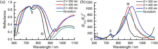
Figure 4. (a) The simulated reflectance spectra and (b) the electric field enhancement (|Emax/E0|2) versus wavelength for three X-Q3D-PNAs with the depths of 350, 400, and 450 nm and one nanostructure without the bottom gold nanodisks. All other parameters are the same as those used in figure 1.
Download figure:
Standard imageLike for other plasmonic elements with sharp vertices such as triangle [33, 34] and bow-tie arrays [35, 36], the electric field is greatly enhanced from 1064 to 1672 when the curvature of the tips of the cross-sectors of x-shaped nanohole is reduced from 40 to 5 nm (figure S4 in the supporting information available at stacks.iop.org/Nano/23/405201/mmedia). The length of the x-shaped nanohole also affects the reflectance spectra and electric field enhancement but this effect is not as significant as that of the width of the x-shaped nanohole, especially for mode III. When the length is changed from 370 to 470 nm, the wavelength of dip III only changes by about 20 nm (figure S5 in the supporting information available at stacks.iop.org/Nano/23/405201/mmedia), which is much smaller than the wavelength shift of about 140 nm when the width is changed from 100 to 160 nm.
3.3. The dependence of the plasmonic properties on the incident angle and polarization
Many applications of plasmonics such as SERS and light harvesting in photovoltaic devices require the enhancement of electric fields with a large tolerance to the light incident angle [39]. It is interesting to investigate the dependence of the incident angle of the enhancement of electric fields due to LSPR mode III. The incident angle was chosen to be co-planar with the wavevector k and the electric vector E, which can greatly influence the coupling condition of BW-SPPs as indicated in equation (1). Figure 5(a) shows the simulated reflectance spectra and the electric field enhancement with the incident angles of 0, 10, 20, and 30° obtained from the X-Q3D-PNA with the dimensions the same as those used in figure 1. As expected, the wavelengths of the SPR modes I and II vary dramatically due to the change of the coupling condition of BW-SPPs caused by different incident angles and we even find new modes appearing according to equation (1). In contrast, the wavelength of the LSPR mode III has a small blue shift with the increasing incident angle. Figure 5(b) shows that the electric field enhancement due to mode III remains almost the same when the incident angle changes from 0° to 20°. The electric field profiles of mode III at the top gold/air interface are shown in figure 5(c) for three incident angles. It is interesting to see that the electric fields are still well confined at the tips of x-shaped intersects with slightly stronger fields on the side facing the electric vector of the inclined incident light. The large incident angle tolerance of LSPR mode III makes the X-Q3D-PNAs excellent SERS-active substrates for microscopic Raman applications, where objectives with large numerical aperture (high incident angle) are used.
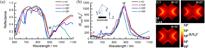
Figure 5. (a) The simulated reflectance spectra and (b) the electric field enhancement (|Emax/E0|2) versus wavelength for the light incident angles of 0°, 10°, 20°, and 30°. (c) The electric field profiles of LSPR mode III at the top gold/air interface resulted from the light illumination with the incident angles of 10°, 20°, and 30°.
Download figure:
Standard imageThe polarization dependence of the reflectance spectra and electric field profiles of X-Q3D-PNAs was also investigated by means of FDTD simulations. Figure 6(a) shows that the reflectance spectra are identical when the polarization rotates from 0° to 45° with respect to the x-direction. Due to the C4v symmetry of the x-shaped plasmonic elements and their square grating arrangement, the 0°–45° rotation of the polarization covers the whole range of 0°–360°. With the polarization rotating away from the x-direction, the confined electric fields start to move from the pair of the tips of the x-shaped nanohole along the x-direction to that along the y-direction (figure 6(c)), resulting in a decrease of |Emax/E0|2 (figure 6(b)). Despite the reduction in intensity of the local electric field by half from 0° to 45° polarization, the number of 'hot spots' is doubled, which could still lead to the same enhancement to the Raman scattering.
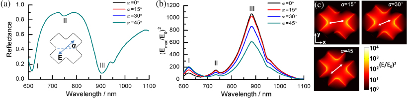
Figure 6. (a) The simulated reflectance spectra and (b) the energy confinement (|Emax/E0|2) versus wavelength for the polarization at 0°, 15°, 30°, and 45° with respect to the x-direction. (c) The electric field profiles at the top gold/air interface resulting from the normal light illumination but different polarizations from 0° to 45° with respect to the x-direction.
Download figure:
Standard image3.4. Experimentally measured reflectance and SERS spectra
The reflectance spectra of X-Q3D-PNAs were experimentally measured. Four X-Q3D-PNAs were fabricated using EBL on the PMMA coated silicon substrates with all the dimensions the same as those in the FDTD simulations shown in (figure 3). The SEM images in figure 7(a) show well fabricated x-shaped nanoholes with the widths of 100, 120, 140, and 160 nm. The experimentally measured reflectance spectra in figure 7(b) show clearly two dips corresponding to modes I and III predicted by the FDTD simulations (figure 3) while the weak dip corresponding to mode II cannot be observed. As predicted by the FDTD simulations, the dips for mode I remain at the same wavelength when the width of the x-shape is increased, while the dips for mode III blue shift because of the decreasing of the length of the gold islands between x-shaped nanoholes in the same rows. The dips in the experimentally measured reflectance spectra are wider than those in the simulated spectra. This phenomenon was also observed in other works [20, 40]. The widening of the dips could be partly due to the factors such as the divergence of collimated light and the roughness of gold surfaces. It is noticed that the dips for mode III are not only wider but also weaker than the prediction of FDTD simulations. This could be due to the slight variation of the size and tip shape of the gold islands fabricated by EBL (figure 7(a)) because mode III corresponds to the LSPRs of gold islands which are very sensitive the size and tip shape of gold islands.

Figure 7. (a) The SEM images of four X-Q3D-PNAs with the widths of 100, 120, 140 and 160 nm fabricated via EBL followed by gold evaporation. (b) The experimentally measured reflectance spectra from these four X-Q3D-PNAs.
Download figure:
Standard imageThe strong electric field enhancement due to LSPR mode III and its large tolerance to the incident angle and polarization can benefit SERS detections. Unlike the 'hot spots' at the narrow gap of gold or silver nanoparticles, the 'hot spots' of X-Q3D-PNAs are at the top open nanoholes where all sizes of analytes of interest can be accessed and easily detected. In addition, the broader wavelength range over which the electric fields are greatly enhanced covers both wavelengths of the laser excitation and the Stokes–Raman scattering of analytes. And most importantly, the enhancements to the excitation and Raman shifts are caused by the same plasmonic mode from the fixed locations, thus enabling very sensitive SERS detections.
Figure 8(a) shows the SERS spectra of 4-MP on the four X-Q3D-PNAs taken with the polarization along the x-direction. The relative enhancement factors are proportional to the SERS peak intensities because all the experimental conditions are the same. The intensities of the ring–breathing vibrational mode coupled with the C–S stretching mode at 1097 cm−1 are 2.2, 5.2, 10.6, and 8.1 kcounts s−1 for the widths of 100, 120, 140 and 160 nm, respectively. The different intensities of SERS signals are completely due to the different electromagnetic enhancements from the X-Q3D-PNAs because the chemical enhancements are the same. The electromagnetic enhancement factor can be estimated from the relationship of (E(ωext)/E0)2(E(ωRaman)/E0)2, where E(ωext) and E(ωRaman) are the electric field energies at the laser excitation wavelength and the Raman vibrational wavelength, respectively [41]. Here, the laser excitation wavelength is 785 nm and the Raman vibrational wavelength is 859 nm for the 1097 cm−1 band. Taking the values of (E(ω=785 nm)/E0)2 and (E(ω=859 nm)/E0)2 for the four arrays, the simulated electromagnetic enhancement factors are 8.4 × 10³, 3.4 × 10⁵, 1.9 × 10⁶, and 4.4 × 10⁶ for the widths of 100, 120, 140, and 160 nm, respectively, based on the results simulated using 0.5 nm mesh in the z-direction. The SERS spectrum of 4-MP SAM on a commercially available SERS substrate (Klarite™) [42] is also shown in figure 8(a). The enhancement of the Raman scattering from the X-Q3D-PNA with the width of 140 nm is about 75 times the enhancement of that from the Klarite substrate. The curvature of the tips of the cross-sectors of x-shaped nanoholes fabricated in this work is about 40 nm, obtained by using an FEI Sirion SEM instrument equipped with Nabity NPGS [25]. Sharper tips can be made by using high end EBL systems. Therefore, even higher SERS enhancement is expected to be achieved as predicted by the FDTD simulations (figure S4 in the supporting information available at stacks.iop.org/Nano/23/405201/mmedia).
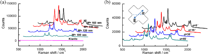
Figure 8. (a) The SERS spectra of 4-MP on four X-Q3D-PNAs taken with normal incident angle and the polarization parallel to the x-direction. The SERS spectrum of 4-MP taken on a Klarite substrate is also shown. A 50 × 0.75 NA objective and a 785 nm laser with the power of 0.3 mW on the sample surface were used. (b) The SERS spectra of 4-MP on the X-Q3D-PNA with the width of 140 nm taken with normal incident angle but varied polarization, from 0° to 45°, with respect to the x-direction. A 10 × 0.3 NA objective and a 785 nm laser with the power of 3 mW on the sample surface were used.
Download figure:
Standard imageThe SERS spectra of 4-MP SAM on the X-Q3D-PNA with the width of 140 nm were taken at different polarization directions from 0° to 45°, shown in figure 8(b). A lower magnification objective of 10 × with a smaller numerical aperture (0.3 NA) was used in order to illuminate a large array area and to reduce the incident angle. The difference of the peak intensities at 1097 cm−1 is less than 10% for the four different polarization directions. As seen in the FDTD simulation results shown in figure 6, although the maxima of |Emax/E0|2 decrease with increasing polarization direction with respect to the x-direction, the number of 'hot spots' is increased. Therefore, the SERS spectra show the same overall enhancement for different polarizations.
4. Conclusions
In summary, we have demonstrated that X-Q3D-PNAs can strongly confine the electromagnetic energy to the tips of the cross-sectors of the x-shaped nanoholes. The FDTD simulations reveal that this strong energy confinement is due to the resonance of LSPPs generated at the gold islands formed between x-shaped nanoholes in the same rows. Both the resonance wavelength and the intensity of the electric field enhancement remain unchanged when the light incident angle changes from 0° to 20°. Rotating the polarization from the direction parallel to the x-shape intersect to that parallel to the x-shape arm, the resonance wavelength remains the same. Although the intensity of the maximum local electric field is reduced due to the polarization change, the electric fields are enhanced at all four tips, instead of just two, of the cross-sectors of the x-shaped nanohole. The broad range of the resonance wavelength and the fixed locations of the enhanced electric fields make the X-Q3D-PNAs excellent substrates for SERS applications because both excitation and Stokes–Raman scattering can be enhanced at the same 'hot spots'. The SERS experiments demonstrate that X-Q3D-PNAs offer about 75-fold higher enhancement compared to the commercially available SERS substrate and the signals remain the same regardless of the polarization direction. Given the large tunable capacity of both wavelength and energy confinement by simply changing the size and spatial arrangement of the plasmonic elements, X-Q3D-PNAs should be of interest for plasmonic applications utilizing strong field enhancement and variable incident angle and polarization such as wide angle light absorbers, photovoltaic devices, and biosensors.
Acknowledgments
This work was supported in part by the American Chemical Society Petroleum Research Funds (ACS PRF) and the University of Washington (UW) faculty start-up funds. DQW acknowledges a fellowship from the China Scholarship Council. EBL and Raman experiments were performed at the Nanotech User Facility, the UW site of the National Nanotechnology Infrastructure Network (NNIN) supported by the NSF.
Footnotes
- 4
Lumerical FDTD solution 7.