
Abstract
A facile route for aligning randomly oriented nanowires synthesized by a vapor–liquid–solid method for the fabrication of nanoelectronic devices was achieved using a polymer combing technique. By controlling the Young's modulus of the polymer combs, van der Waals interactions and shearing forces between the combs and nanowires can be manipulated and thus the nanowire density and alignment can be controlled. Using the proposed method, field-effect transistors were directly fabricated on as-grown substrates after aligning the nanowires, thereby demonstrating the feasibility of the scheme for the production of nanoelectronic devices.
Export citation and abstract BibTeX RIS
1. Introduction
One-dimensional nanomaterials [1] such as carbon nanotubes and semiconductor nanowires (NWs) have been extensively explored as building blocks in electronic [2–4], optoelectronic [5], photovoltaic [6], and biological devices [7] due to their unique physical properties that arise as a result of their low dimensions.
Growth methods and mechanisms based on bottom-up processes such as the vapor–liquid–solid (VLS) technique have been widely used for the production of high-density NWs with controllable diameters and lengths. The fabrication of coaxial and branched NWs [8] has also been reported by several research groups. The radial or branched junctions present in such structures allow the electronic [9] and photovoltaic [10, 11] performance to be improved.
The up-scaling of NW-integrated devices is still challenging due to difficulties in assembling and ordering entangled meshes of bottom-up grown NWs at desired locations. Thus, NW devices have usually been realized via top-down approaches, such as lithography followed by etching on crystalline thin films. However, such schemes require complicated fabrication procedures, and the crystal structure of the NWs can be damaged during physical etching processes.
Bottom-up NWs have also been investigated as a channel material for low-cost, flexible electronics because of their flexibility and mechanical strength. Conventional complementary metal–oxide semiconductor (CMOS) fabrication processes cannot be used for flexible electronics due to the thermal instability of plastic substrates. Therefore, the transfer and alignment of bottom-up grown NWs on flexible substrates is a fascinating route to realize high-performance flexible electronic devices.
Several approaches have been developed to overcome the disordering problems of bottom-up grown NWs. Electric field-driven alignment [2] and optical traps [12] were used to guide randomly distributed NWs in solution to an electrode with high precision, but the method yielded NWs with a low density. Fluidic alignment combined with surface patterning was also employed to align NWs into parallel arrays [13]. The method produced ordered NW arrays with a high density in some areas. The ordered growth of NWs along a specific orientation of substrates such as sapphire has been reported, but the scheme is specific to a given material and substrate [14]. Wafer-scale NW contact printing has yielded a high density (∼10 NWs μm−1) of aligned NWs on arbitrary substrates via shearing, but precise control over the post-fabricated electrodes is difficult for the production of large-scale devices [15].
Here, we report on a simple approach for the large-scale integration of entangled semiconductor NWs by pre-positioned growth and subsequent roller combing of the NWs. The fabrication of highly ordered, parallel, and dense arrays of semiconductor NWs on source substrates was demonstrated, and a viable NW metal–oxide semiconductor field-effect transistor (MOSFET) was produced.
2. Experimental details
Ge NW growth was performed using a custom-made chemical vapor deposition (CVD) system with a single zone heating furnace (Lindberg Blue). Gold nanoparticles (15 nm) were first immobilized on a photolithographically patterned Si/SiO2 wafer using 0.1% w/v poly-L-lysine in water (Ted Pella Inc.). The nanoparticles functioned as a catalyst for the VLS growth of Ge NWs on the patterned catalyst area. Before growth, the wafer was placed in the quartz tube of a tubular furnace with a single heater, and the growing temperature was set to 280 ° C under a 20 sccm flow of H2. After reaching the desired temperature, the gas was switched from H2 to 15 sccm of GeH4 (10% balance with H2) gas for 20 min.
InAs NWs (∼30 nm diameter and ∼20 mm length) were synthesized via VLS growth with Ni nanoparticles as a catalyst and solid InAs powder as the source material [16]. During this process, ∼10 nm Ni nanoparticles were produced from ∼0.5 nm-thick Ni films by annealing at 850 ° C for 10 min in a hydrogen environment. The InAs source powder was then annealed at 720 ° C for 1 h while the sample substrate with the Ni catalyst was held at 470 ° C. During growth, 150 sccm of hydrogen gas was used to deliver the thermally evaporated InAs.
Polydimethylsiloxane (PDMS) combing rollers with different Young's moduli were prepared from curing solutions with different s-PDMS (Sylgard 184, Dow Corning)/h-PDMS (VDT-731, HMS-301, SIP 6831.2, Gelest) ratios. Glass tubes with a 1 cm diameter were first treated with vaporized (tridecafluoro-1,1,2,2-tetrahydrooctyl)-1-trichlorosilane (Gelest) for 1 h so as to form an anti-sticking layer inside the tubes. The s- and h-PDMS mixtures were then cured in the glass tube for 2 h at 70 ° C, and the resulting PDMS rollers were subsequently separated from the tube.
Entangled NWs grown on pre-patterned Au catalysts on Si/SiO2 (50 nm thick) substrates were combed using the PDMS rollers. The PDMS rollers were placed in contact with the NW substrate and then slid in the desired direction with a gentle pressure (∼10 g cm−2). Constant pressure could be applied during polymer combing using a stage with a spring underneath, but gentle hand pressure could also produce NWs with small differences in the density and the alignment of NWs. FETs were also fabricated by the deposition and lift-off of metal on the pre-opened photoresist patterns.
3. Results and discussion
Figure 1 shows how the NWs grown in random directions can be planarized and aligned parallel to the substrates via the polymer combing technique. Patterned crystalline Ge or InAs NWs on Si/SiO2 (50 nm thick) wafers were first prepared by the VLS process on lithographically patterned Au catalyst lines (2 μm × 100 μm lines with 30 μm spacing). PDMS rollers were then placed in conformal contact with the NW substrates along the catalyst lines. Finally, the PDMS roller was slid perpendicular to the catalyst lines under the application of a ∼10 g cm−2 normal pressure. After sliding the PDMS roller, the NWs were 'knocked down' and aligned along the sliding direction by the applied shearing forces.
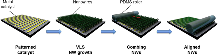
Figure 1. Schematic of the NW combing process. Semiconductor NWs are first grown on patterned catalyst lines by the VLS process. A PDMS roller is then placed on the NW substrates along the catalyst lines. After sliding the roller with gentle pressure, the NWs are aligned along the sliding direction.
Download figure:
Standard image High-resolution imageTo examine the alignment after combing, optical images acquired before and after combing were compared (figure 2). Ge NWs with a length of approximately 20 μm (∼30 nm radius) on Si/SiO2 were non-epitaxially grown on the Au catalyst lines (figure 2(a)). The spacing between the catalyst lines was 30 μm so as to prevent undesired overlapping of neighboring NWs, which can induce junction resistance. The empty spaces are large enough for the direct integration of global back gate electrodes. After combing, the NWs were flattened and aligned on the surface of the Si/SiO2. The region of the NWs immediately adjacent to the catalyst lines was slightly separated from the substrates because the rough catalyst lines interfere with shearing contact between the NWs and the substrates. However, most of the NWs are in contact with the substrate for the facile fabrication of the contact electrode. The density of the NWs was similar to the original NW density, and no fractured NWs were observed.

Figure 2. Optical microscopy images of the GeNWs (a) before and (b) after polymer combing.
Download figure:
Standard image High-resolution imageCompared to knocking down a single NW grown normal to the substrate, it is more challenging to achieve good alignment by combing entangled NWs [17]. The selection of proper combing materials is a prerequisite for achieving good alignment of high-density NWs. Hard materials such as metal, plastic, glass, and Si wafers are not appropriate for combing because the application of a preload on the brittle crystalline NWs with a hard substrate can form defects or cracks in the NWs. Furthermore, the fabrication of NWs with a rough surface due to the use of a metal catalyst hinders uniform contact between the hard substrate and the NWs, which leads to inhomogeneous shearing force transfer during the combing process. For this reason, polymers have become a good candidate for the combing of NWs. First, polymers are soft materials and thus they have the ability to release strain in the brittle NWs. For example, soft polydimethylsioxane (s-PDMS) has been used to transfer crystalline NWs onto arbitrary substrates [18]. Second, the polymer itself is very smooth after curing on a smooth substrate, and its softness can facilitate conformal contact with the NWs upon the application of a small preload. Lastly, shearing adhesion can be controlled by choosing polymers with different Young's moduli.
The Young's modulus of the combing polymer is a crucial factor to achieve good alignment and prevent fracture of the NWs. There is a trade-off between the alignment and density of the NWs in the polymer combing process. Soft polymers with a low Young's modulus are ideal for aligning the NWs due to their high shearing force. However, van der Waals interactions between low Young's modulus polymers and the NWs are excessively high and thus conformal contact of the low Young's modulus polymers detaches the NWs from the source wafers. In contrast, relatively weak van der Waals interactions are present between high Young's modulus polymers and the NWs. Consequently, fewer NWs become attached to the polymer roller. However, alignment of the NWs is sacrificed for a high NW density because of weak shearing forces.
PDMS is a good combing material because its Young's modulus can be controlled by simply changing its composition. Here, the PDMS solutions were cured in glass tubes with an anti-sticking layer (modified with (tridecafluoro-1,1,2,2-tetrahydrooctyl)-1-trichlorosilane) to create PDMS rollers (diameter = 1 cm,length ∼ 10 cm, figure 3(a)). Compared to a flat PDMS slab, cylindrical PDMS rollers were considered so as to minimize the tangent contact area between the NWs and PDMS. To control the Young's modulus, a mixture of low Young's modulus PDMS (s-PDMS, modulus: 1.5 MPa) and high Young's modulus PDMS (h-PDMS, modulus: 9 MPa) was employed. By increasing the amount of h-PDMS, we can proportionally increase the Young's modulus of the PDMS from ∼1.5 MPa (s-PDMS only) to 5 MPa (figure 3(b)). A roller with a composition of 100% h-PDMS could not be used to comb the NWs because it was too brittle when removed from the glass tube template.
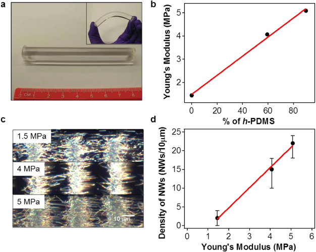
Figure 3. NW combing density modulation according to the Young's modulus of the PDMS roller: (a) optical image of the PDMS roller, (b) plot of Young's modulus with respect to the percentage of h-PDMS in the PDMS roller, (c) optical images of NWs combed with PDMS rollers having different Young's moduli, and (d) plot of the NW density with respect to the Young's modulus of the PDMS roller.
Download figure:
Standard image High-resolution imageFigures 3(c) and (d) show how the Young's modulus of the PDMS roller can affect the density of aligned NWs. The density of the NWs is linearly proportional to the Young's modulus of the PDMS rollers. For the 5 MPa roller, the NW density was 22 NWs/10 μm, while a density of 2 NWs/10 μm was achieved when a 1.5 MPa PDMS roller was employed. The 1.5 MPa PDMS roller imparts a high shearing force, and thus the NWs became detached or were cracked during the combing process (figure 3(c)). In contrast, the high Young's modulus PDMS roller imparts lower shearing forces and the tangent contact with the source wafer is smaller under the same applied normal pressure. Consequently, the density of combed NWs was higher [19].
Combed NWs on source wafers can be transferred to polymer substrates with a high yield in order to fabricate flexible electronic devices. Flexible NW FETs have attracted a great deal of attention due to their potential application as artificial e-skins [20], flexible displays [21], and rollable photovoltaics [22]. High-density NW integration on plastic substrates using conventional transfer methods is still challenging because of the native surface properties of plastics, namely their hydrophobicity and roughness. NW alignment on a flexible film (Kapton) by printing has been demonstrated in previous research, but the transfer yield was low. With our approach, a high yield can be achieved by curing the polymer directly on the combed NW source wafers. Here, a polyimide (PI) solution was first spin-coated at 1000 rpm onto the source wafer (2 cm × 2 cm) with combed Ge NWs, and then the assembly was cured in a vacuum convection oven at 250 ° C for 1 h (figure 4(a)). After cutting the edge of the cured PI films, the film was easily peeled off from the source wafer. Comparing the number of NWs remaining on the source wafer before and after Kapton transferring, the combed Ge NWs were ultimately transferred to the PI film with a high yield and an ordered shape (figure 4(b)).
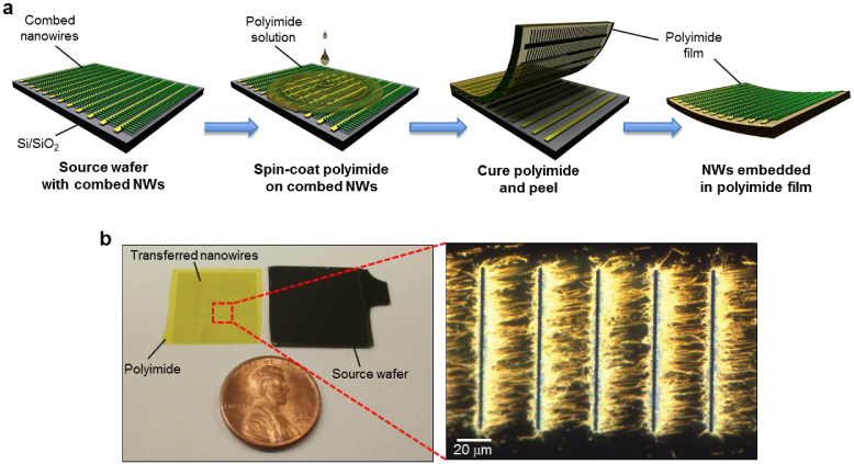
Figure 4. Kapton transfer of combed NWs for flexible electronic devices: (a) process schematic of the Kapton transfer of combed Ge NWs; (b) optical image of a Kapton film with aligned Ge NWs (inset) transferred from a combed Ge NW source wafer.
Download figure:
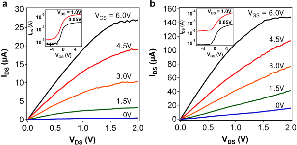
Standard image High-resolution imageFor proof-of-concept purposes, NW FETs were fabricated on a Si/SiO2 (50 nm thick SiO2) wafer using combed InAs NWs as the active channel material. The InAs NWs with a 30 nm diameter were grown via VLS on electron beam-evaporated Ni catalyst lines (0.5 nm thickness). The as-grown InAs NWs were combed by sliding a PDMS roller (5 MPa Young's modulus) under a normal pressure of ∼10 g cm−2. Following the InAs NW combing, FETs with a common back-gated geometry were fabricated by patterning Ni (∼50 nm-thick) source (S) and drain (D) metal contacts (∼3 μm spacing) so as to produce bridges between the combed NWs on the Si/SiO2 substrate. The output (IDS–VDS) and transfer characteristics (IDS–VGS) of FETs consisting of a single InAs NW and multiple NWs are shown in figures 5(a) and (b), respectively. The single InAs NW FET exhibited an ON-current of up to Ion ∼ 10 μA at VDS = 1 V with an Ion/Ioff ratio of ∼104 (figure 5(a)). On the other hand, the multiple NW FETs showed a higher ON-current of Ion ∼ 100 μA at VDS = 1 V with an Ion/Ioff ratio of ∼102. However, the current (Ion) divided by the width of the S/D contacts was ∼1 μA μm−1 at VDS = 1 V, indicating that few NWs were connected to the S/D. This relatively low current level can be mainly attributed to variation in the lengths of NWs, which are shorter than the distance between the S/D, during the growth process. In addition, it can also be attributed to the high NW-to-Ni contact resistance induced by PDMS residue remaining after the combing process and non-ideal gate coupling of the imperfectly anchored NWs on the SiO2 surface. It should also be noted that the lower Ion/Ioff ratio of the multiple NW FETs was induced by a difference in the threshold voltages of NWs with different diameters (figure 5(b)). We expect that the performance of this device can be further improved by optimizing the NW growth process and combing process. We demonstrated the feasibility of a combing method for achieving NW FETs with reliable performance. The proposed scheme could be employed for the on-chip integration of various NWs, including Ge and InAs NWs.
Figure 5. InAs NW FET based on combed NW arrays: IDS–VDS characteristics of NW FETs consisting of (a) single InAs NWs and (b) multiple combed InAs NWs measured at different VGS values from 0 to 6.0 V. The inset shows IDS–VGS characteristics of the same device measured at VDS = 0.05 and 1.0 V.
Download figure:
Standard image High-resolution image
4. Conclusions
A simple and general polymer combing approach was developed to directly align semiconductor NWs on as-grown wafers. The combed NWs were aligned along the grown substrate with a controllable density, and then subsequently transferred to flexible substrates with high yield. Finally, a field-effect transistor was successfully fabricated on the combed NWs, thereby demonstrating the viability of our combing method in the design of NW electronics.
Acknowledgments
This research was supported by the Basic Science Research Program through the National Research Foundation of Korea (NRF) funded by the Ministry of Science, ICT & Future Planning (No. NRF-2012R1A1A1015659). The authors would like to thank Professor Junghyo Nah at Chungnam National University, Korea and Professor Kuniharu Takei at Osaka Prefecture University, Japan for helpful discussions.