
Abstract
High quality ZnO nanowires (NWs) were grown on a graphene layer by a hydrothermal method. The ZnO NWs revealed higher uniform surface morphology and better structural properties than ZnO NWs grown on SiO2/Si substrate. A low dark current metal–semiconductor–metal photodetector based on ZnO NWs with Au Schottky contact has also been fabricated. The photodetector displays a low dark current of 1.53 nA at 1 V bias and a large UV-to-visible rejection ratio (up to four orders), which are significantly improved compared to conventional ZnO NW photodetectors. The improvement in UV detection performance is attributed to the existence of a surface plasmon at the interface of the ZnO and the graphene.
Export citation and abstract BibTeX RIS
1. Introduction
Zinc oxide (ZnO) material has recently been extensively investigated and has shown great promise for ultraviolet (UV) photodetectors (PDs) due to its intrinsic properties such as wide bandgap, high UV absorption coefficient, low cost, etc [1–5]. Due to their large surface-to-volume ratio, ZnO nanowires (NWs) exhibit great applicability to high sensitivity and fast response UV sensors [6, 7]. ZnO NWs have been successfully grown on solid substrates by various methods such as the vapor–liquid–solid (VLS) process, metal organic chemical vapor deposition (MOCVD) and chemical oxidation [8–11]. ZnO NWs are mostly grown on silicon, sapphire or glass substrates. There is great interest in synthesizing ZnO NWs on graphene because its excellent thermal and electrical conductivity can potentially improve the electronic and optoelectronic properties of the ZnO [12, 13]. Various graphene-based composite nanomaterials have proved to be promising for a wide range of applications such as catalysis, optoelectronic and energy conversion, and storage devices [14–19]. However, to the best of our knowledge, no one has focused on research on metal–semiconductor–metal (MSM) ultraviolet detectors based on ZnO NW growth on graphene layer substrate.
In this paper, we report a simple and low cost method to grow large scale well aligned ZnO NW arrays on a graphene layer at a low temperature. The properties of the ZnO NWs were systematically investigated by x-ray diffraction (XRD), scanning electron microscopy (SEM), Raman spectroscopy and photoluminescence (PL). An MSM structured PD based on ZnO NWs has also been fabricated. This device exhibits a dark current of 1.53 nA at 1 V bias, and a large ratio of photocurrent to dark current and UV-to-visible rejection ratio (up to four orders). The significant UV detection improvement of the PD is mainly due to the existence of a surface plasmon at the interface between the graphene and the ZnO NWs.
2. Experimental procedures
High quality graphene films were synthesized by CVD on the interior surface of Cu foil enclosures. The base pressure of the CVD chamber was 1.5 mTorr, and the temperature was kept at 1035 ° C. After graphene growth, the graphene-on-Cu sample was spin coated with poly-methylmethacrylate (PMMA). Then the Cu substrate was dissolved in an (NH4)2S2O8 solution and the PMMA–graphene was lifted from the solution and transferred onto p-type silicon substrate with a SiO2 layer of about 300 nm thickness. After transfer, the PMMA–graphene was immersed in acetone solution to remove the PMMA.
For the growth of ZnO NWs, a ZnO seeding layer of approximately 40 nm thickness was deposited on oxidation p-type Si substrates with RF magnetron sputtering using a 99.99% ZnO target at room temperature. Then the ZnO seeding substrates were placed into a reaction solution containing 0.66 g Zn(NO3)2⋅6H2O and 0.35 g hexamethylenetetramine (HMTA) dissolved in 100 ml deionized water and maintained at 90 ° C for 1 h.
Interdigitated finger MSM PDs were fabricated by standard photolithography and liftoff techniques. The optical active area was 200 × 300 μm2 with 3 μm finger width and 10 μm spacing. Au was employed as the metal contact and was deposited by magnetron sputtering with a thickness of 200 nm. The current–voltage (I–V) curves were obtained using a Keithley 2410 sourcemeter and a Keithley 6514 electrometer, and measured at room temperature. The light current was obtained at 370 nm UV light of intensity 0.215 μW. The synthetic procedure for the production of ZnO NWs and a schematic diagram of the ZnO NW MSM detector structures are illustrated in figure 1.

Figure 1. The fabrication steps and a schematic diagram of ZnO MSM detector structures. Firstly, a bilayer of graphene was transferred to an oxidation p-type silicon substrate, then high quality ZnO NWs were grown on the graphene layer by a hydrothermal growth method. Finally, Au–ZnO–Au MSM structure PDs were fabricated by standard photolithography and liftoff techniques.
Download figure:
Standard image High-resolution image3. Results and discussion
The crystalline quality and orientation of ZnO nanowires grown on an oxidation silicon substrate and a graphene layer were investigated by XRD, as shown in figure 2. For the samples, the diffraction peaks at 31.80°, 34.47°, 47.78° and 56.38° are ascribed to ZnO (100), (002), (102) and (110) crystal planes of the hexagonal wurtzite structure of ZnO, respectively (JCPDS 65-3411). The stronger (002) diffraction peak of the ZnO NWs indicates a preferential vertical growth direction. It is noted that the intensity of the (002) diffraction peak significantly increases while the full width at half maximum of the (002) diffraction peak decreases for the ZnO NWs grown on the graphene layer compared to growth on the SiO2/Si substrate. This implies that the crystal quality is improved at the graphene layer, which is attributed to the smaller lattice constant between graphene and ZnO [20, 21].
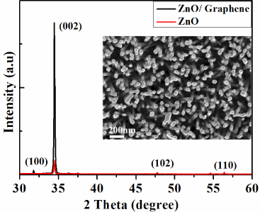
Figure 2. XRD pattern of the ZnO NWs and ZnO NW growth on graphene. The inset shows an SEM image of ZnO NW growth on a graphene layer by a hydrothermal method.
Download figure:
Standard image High-resolution imageThe surface morphology of the synthesized ZnO NWs was investigated by SEM. The inset image of figure 2 shows a plane view SEM image of a highly aligned, vertical ZnO NW array grown on a graphene layer. High density ZnO NWs with an average diameter of approximately 45 nm grew nearly vertically on the graphene layer. Most of the ZnO NWs exhibited a hexagonal shape, demonstrating the high quality of the ZnO crystals and their c-axis growth along the (0001) plane, which is consistent with the XRD measurement.
The Raman spectra of ZnO NW growth on a SiO2/Si substrate and a graphene layer are shown in figure 3(a). In figure 3(a), we observe two giant peaks at 306 and 520 cm−1 and a weak peak at 615 cm−1, which correspond to the silicon substrate. A strong Raman peak at 436 cm−1 corresponds to E2 (high). From the spectra, it can be seen that the E2 (high) mode shifts slightly to 440 cm−1 for ZnO NW growth on a SiO2/Si substrate. The broad and weak peaks at 330 and 669 cm−1 seen in both spectra in figure 3(a) are attributed to the second Raman process [22, 23]. The accurate position for the Raman modes in figure 3(a) indicates the higher crystal quality of the ZnO NW growth on graphene than on SiO2/Si substrate. Figure 3(b) shows the Raman spectra of graphene before and after growth of ZnO NWs; three peaks centered at around 1350, 1585 and 2710 cm−1, corresponding to the D, G and 2D modes are observed. It is well known that the ratio of the intensities (ID/IG) provides a sensitive measure of the disorder and crystalline size of the graphene layers. A weak D mode is detected in the Raman spectra of transferred graphene, which means a small number of defects. However, the intensity of the D peak increases rapidly while the ZnO NWs grow on the graphene layer. The distinctive increase in the peak intensity ratio ID/IG for the growth of ZnO NW samples indicates that a number of defects have occurred during the ZnO NW growth process [20, 24, 25]. This is due to the structural damage incurred by the graphene layer during the sputtering seeding process [4, 13]. In addition, the intensity ratio of the G and 2D modes correlates with the number of graphene layers. The intensity ratio of the G and 2D modes of around 1.3 for the samples before and after ZnO NW growth is associated with bilayer graphene [18].
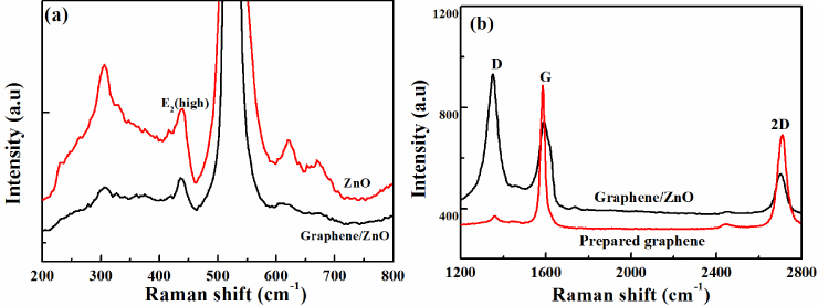
Figure 3. (a) Raman spectra of ZnO NW growth on a SiO2/Si substrate and a graphene layer and (b) Raman spectra of graphene before and after growth of the ZnO NWs.
Download figure:
Standard image High-resolution imageFigure 4 shows the room temperature PL spectra of ZnO NWs grown on a graphene layer or on a silicon dioxide substrate. The PL spectra were excited by a 248 nm KrF laser in air. From the spectra, we can see a sharp and strong photoemission peak at about 386 nm, which is ascribed to the bandgap emission of ZnO material. A weak peak located at approximately 544 nm has been observed for the PL spectra of ZnO NWs grown on silicon dioxide substrate. It has been established that the visible emission from ZnO in the blue–green region originates from defect states related to oxygen in the ZnO films [10]. However, we could not observe defect emission or the defect emission was below the detection limit. The significant enhancement of bandgap emission and disappearance of defect emission can be attributed to the improvement of crystalline quality [18] and the existence of a surface plasmon on the surface of the interface [26], which is in good agreement with XRD and Raman measurements.
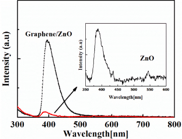
Figure 4. Room temperature photoluminescence spectra of ZnO NWs grown on a graphene layer and on a silicon dioxide substrate.
Download figure:
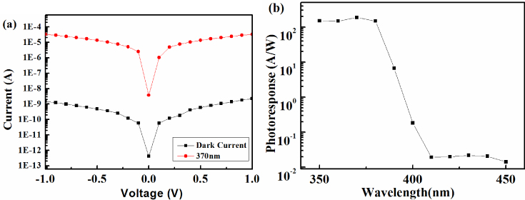
Standard image High-resolution imageAccording to previous reports, ZnO material-based PDs are highly responsive to 370 nm UV light; here, we examined the I–V characteristics for the UV PDs under illumination with 370 nm UV light at a power intensity of 0.215 μW and in the dark. The optical active area was 200 × 300 μm2. The I–V curves of the ZnO NW MSM PDs are shown in figure 5(a). A uniform Schottky contact between the Au electrodes and the ZnO NWs is revealed by the symmetry of the I–V curves. We observed that the device exhibited a very low dark current of 1.53 nA at 1 V bias. The light current increased to 3.4 × 10⁻⁵ A at 1 V bias, when the 370 nm UV light was used to irradiate the fabricated PDs. The ratio of the photocurrent to the dark current was about four orders, while the intensity of irradiation was 370 nm UV light at 0.215 μW.
Figure 5. (a) I–V characteristics of MSM PDs fabricated with ZnO NWs grown on a graphene layer in the dark and under illumination with a 370 nm UV light with an incident power density 0.215 μW. The optical active area was 200 × 300 μm2. (b) Spectral response of the ZnO NW MSM PDs at 1 V bias.
Download figure:
Standard image High-resolution image
The current transport over the Schottky barrier is explained well by thermionic emission theory using the following general equations:

where
Here I0 is the reverse saturation current, q is the electron charge, V is the bias voltage, η is the ideality factor, A* is the effective Richardson constant, which has a theoretical value of 32 A cm−2 K−2, S is the contact area, and ΦB is the effective Schottky barrier height [26–28]. By fitting the forward I–V curve, the barrier height and ideality factor were determined to be 0.88 eV and 1.63, respectively. The value of ΦB is approximately equal to the theoretical distance between the Au work function of 5.1 eV and the ZnO electronic affinity (4.2 eV) [29]. This confirms the very limited Fermi level pinning effect at the Au/ZnO interface. Figure 5(b) illustrates the spectral response for the ZnO NW MSM PD at 1 V bias. The device shows a cutoff wavelength at about 390 m, which corresponds to the optical absorption gap of ZnO. At 1 V bias, the highest responsivity is 188 A W−1 for the incident light wavelength of 370 nm, and average responsivity is 0.02 A W−1 for an incident visible light wavelength from 410 to 450 nm. The UV-to-visible rejection ratio for the ZnO MSM NW PD is about four orders. The error scale is limited to 5%.
PDs fabricated on the ZnO NWs grown on graphene have a better dark current, ratio of photocurrent to dark current, and UV-to-visible rejection ratio compared to the PD devices based on ZnO NWs that were grown on SiO2/Si substrate (by about one to two orders, data not given here). The improvement of UV PDs based on ZnO NWs can be attributed to two factors: improvement of crystalline quality and the surface plasmon from the graphene and ZnO interface. The crystal quality of ZnO NWs grown on graphene is better than that of ZnO NWs grown on SiO2/Si substrate; this result has been demonstrated by the above experimental data.
Recently, a surface plasmon has been demonstrated on the interface between a layer of graphene and ZnO [30]. The surface plasmon excites an electromagnetic field in ZnO NWs. According to previous reports [31], the peak amplitude of the surface plasmon-induced electromagnetic field is expected to be much greater than that of the incident electromagnetic field. Thus, the increased field amplitude and increased interaction time between the field and the ZnO NWs would be expected to increase the absorption of incident electromagnetic energy. For our device, increased optical absorption due to the presence of graphene will be manifested as an increase in photocurrent response at wavelengths corresponding to those of the graphene surface plasmon resonances.
Meanwhile, it is widely accepted that the photoconduction mechanism of ZnO NWs functions as follows. In a dark atmosphere, oxygen molecules are absorbed on the material's surface and capture the free electrons from the ZnO:
A low-conductivity depletion layer is formed near the surface. After UV light illumination, electron–hole pairs are photo-generated, and then the photo-generated holes migrate to the surface and discharge the negatively charged adsorbed oxygen ions:
Consequently, oxygen is photo-desorbed from the surface. The unpaired electrons are either collected at the anode or they recombine with holes generated when oxygen molecules are reabsorbed and ionized at the surface [32, 33]. Pan et al [34] reported that the photo-excited electrons in the conduction band of ZnO NWs can transfer to the graphene, which acts as an electron sink due to the Schottky barrier at the graphene–ZnO interface. In turn, the charge separation prevents the recombination of electrons and holes; thus, as many photo-generated carriers as possible can be collected which results in improved responsivity.
4. Conclusion
In conclusion, we have grown high quality ZnO NWs on a graphene layer by a hydrothermal method. The XRD, SEM, Raman and PL spectra of the ZnO NWs demonstrate the high crystal quality of the ZnO NWs. Additionally, ZnO NW MSM PDs with Au Schottky contacts have been fabricated. The PDs exhibit a very low dark current of 1.53 nA at 1 V bias, and a large ratio of photocurrent to dark current and UV-to-visible rejection ratio (up to four orders). The enhanced detector performance is due to the improvement of ZnO NW crystal quality, the increase in optical absorption, and the prevention of electron–hole recombination caused by the surface plasmon from the graphene and ZnO interface.
Acknowledgments
This work was supported by the National Natural Science Foundation of China (Grant Nos 61176049 and 61307047) and the Program for New Century Excellent Talents in Fujian Province University (NCETFJ). The authors also acknowledge the financial support award from China Scholarship Council (CSC). Thanks are due to Samantha Riley at UC San Diego for carefully polishing the English of this paper.