

Abstract
Artificial monolayer black phosphorus, so-called phosphorene, has attracted global interest with its distinguished anisotropic, optoelectronic, and electronic properties. Here, we unraveled the shear-induced direct-to-indirect gap transition and anisotropy diminution in phosphorene based on first-principles calculations. Lattice dynamic analysis demonstrates that phosphorene can sustain up to 10% applied shear strain. The bandgap of phosphorene experiences a direct-to- indirect transition when 5% shear strain is applied. The electronic origin of the direct-to-indirect gap transition from 1.54 eV at ambient conditions to 1.22 eV at 10% shear strain for phosphorene is explored. In addition, the anisotropy diminution in phosphorene is discussed by calculating the maximum sound velocities, effective mass, and decomposed charge density, which signals the undesired shear-induced direct-to-indirect gap transition in applications of phosphorene for electronics and optoelectronics. On the other hand, the shear-induced electronic anisotropy properties suggest that phosphorene can be applied as the switcher in nanoelectronic applications.
Export citation and abstract BibTeX RIS
1. Introduction
The discovery and investigation of graphene with two dimensional (2D) hexagonal honeycomb carbon promotes the emergence of 2D materials [1, 2]. Apart from graphene, many novel 2D materials, for instance, elementary silicene and germanene, functional graphene, silicene, and germanene [3, 4], binary single-layer boron-nitride [3], as well as monolayer transition metal dichalcogenides [5], have attracted global interest. The fascinating and unexpected electronic, optical, mechanical, magnetic, and thermal properties of these low-dimensional materials provide unlimited possibilities for artificial materials and potential applications. For example, functionalized germanenes were predicted to be topological insulators with finite 2D bandgaps and one-dimensional (1D) gapless edge states [6]. Monolayer boron-nitride [3] and MoS2 [7], as well their related 2D van der Waals heterostructures [8, 10], were designed as photocatalysts in the applications of visible light-induced, water- splitting hydrogen production.
Very recently, monolayer black phosphorus, or phosphorene, has been fabricated [11, 13] and has attracted increasing interest due to its peculiar anisotropic, optoelectronic, and electronic properties [14, 20]. Potential applications such as nanoelectronic transistors [12], solar cells [18], and photocatalysts [21] have been proposed for this novel mono-elementary 2D material, which show high carrier mobility [22, 24], a negative Poisson's ratio [25], and enormous mechanical flexibility [26]. Many studies show that the electronic structure of phosphorene is very sensitive to external conditions. For instance, the geometries stabilities, and diffusions of the monovacancy and divacancy in phosphorene have been calculated [27], and the mechanism of the semiconductor-to-metal transition [28] and direct-to- indirect bandgap transition [29] in phosphorene under applied interplanar strains have been theoretically explored. Recently, Fei et al found that the preferred conducting direction in phosphorene can be rotated by appropriate intraplanar biaxial or uniaxial strains [30]. All these previous studies are focused on phosphorene under applied single-axial or biaxial strains. However, the study of phosphorene under shear strain, another very important and commonly used external condition for 2D materials [31, 32], is still lacking. Considering that strain engineering is one of the most important material processing technologies in the semiconductor industry [33], a comprehensive study of shear-strained phosphorene is of great interest and importance as well.
In this work, we systematically studied the crystal and electronic structures of phosphorene under intraplanar shear strains based on density functional theory calculations. The lattice dynamical stability of phosphorene under certain shear strains and the sound speed, as well as structure deformation, were discussed. We further unraveled the electronic origin of the direct-to-indirect gap transition in phosphorene under shear strain. Moreover, the effective mass and decomposed charge density were further studied to uncover the anisotropy diminution in phosphorene.
2. Computational details
The density functional theory (DFT) calculations of phosphorene were based on the Vienna ab initio simulation package [34] in conjunction with projector augmented wave pseudopotentials within the generalized gradient approximations [35] of Perdew–Burke–Ernzerhof [36] (PBE). The valence electron configuration for P was 3s23p3. The geometry convergence was achieved with the cutoff energy of 500 eV. K-points of 8 × 10 × 1 were automatically generated with the Γ symmetry. In order to prevent interaction between periodic images, we introduced a vacuum of 20 Å thickness in the z-axis direction. The relaxation convergence for ions and electrons was 1 × 10⁻⁶ eV. The PHONOPY [37] code was applied to get the phonon frequencies through the supercell approach with a 3 × 6 × 1 supercell and 2 × 2 × 1 K-points. Since the van der Waals interactions in the phosphorene are less significant than the bulk black phosphorous, the van der Waals- corrected optB88 function [38] was applied for comparison only. The Heyd–Scuseria–Ernzerhof (HSE06) hybrid functional [39] with a 25% short-range exchange energy from Hartree–Fock was introduced to evaluate the bandgap of phosphorene under shear strains. The isosurfaces of the decomposed charge density were visualized using the VESTA [40] tool.
3. Results and discussions
The sketch of the crystal structure of phosphorene is presented in figure 1(a); phosphorene has an orthogonal 2D crystal structure. The relaxed lattice parameters a = 4.626 Å and b = 3.298 Å agree well with previous studies [29, 30]. The distortion of the lattice is defined by multiplying the Bravais lattice vectors matrix with the applied shear distortion matrix  where
where  is the applied shear strain. Figure 1(b) shows the schematic diagram of the phosphorene lattice under applied shear strain.
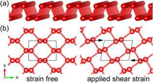
Figure 1. (a) The structure sketch of phosphorene. (b) The schematic diagram of the applied shear strain.
Download figure:
Standard image High-resolution imageFirstly, we explored the stability of phosphorene under applied shear strains. Figure 2 illustrates the phonon dispersion curves of phosphorene under various shear strains. As can be seen in figure 1(a), our calculated phonon dispersion curves for phosphorene without shear strain agree well with the previous studies [41]. Interestingly, even 1% shear strain splits off all the double-degenerated phonon dispersion modes along the X-to-M and M-to-Y directions. Meanwhile, the double-degenerated modes at the X and Y points remain degenerated. However, the splitting of the original degenerated modes does not break the stability of the phosphorene lattice. It can be found that the phosphorene lattice remains stable under up to 10% applied shear strain without any imaginary mode (figures 1(b)–(c)). As the applied shear strain increased into the range from 11–15%, there exhibits fcc ThH2-type [42, 43] imaginary acoustic modes along the Γ-to-X direction and the Γ-to-Y direction, shown in figures 2(d) and (e), although such imaginary modes can be enhanced to positive by the temperature effects or temperature-induced electron—phonon interactions [44]. Such negative dispersion modes indicate the lattice instability of the phosphorene lattice under certain shear strains. By further increasing the applied shear strain to 16% (figure 2(e)), one double-degenerated acoustic phonon mode becoming negative around the Y-to-M direction indicates strong lattice instability, which may lead to the crash of the phosphorene lattice. Since the application of phosphorene must be based on good stability, we will analyze the physical and chemical properties of phosphorene under no more than 10% shear strain in the following part.
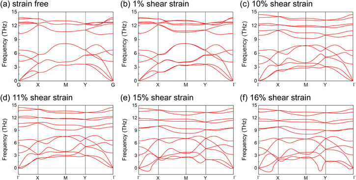
Figure 2. The phonon dispersion curves of phosphorene under (a) 0%, (b) 1%, (c) 10%, (d) 11%, (e) 15%, and (f) 16% shear strain.
Download figure:
Standard image High-resolution imageFor phosphorene, there are four atoms in one unit cell, with three acoustic phonon modes and nine optic phonon modes in the phonon dispersion curves. The optic phonon frequencies at the Γ point are classified according to the irreducible representations. The even parity vibrations 


 and
and  with the inversion symmetry at the Γ point are Raman active modes, and the odd-parity vibrations
 and
and  showing anti-symmetry at the Γ point are infrared modes. More details about the atomic motions of vibrational modes can be found in Fei et al's [45] letter. The calculated phonon frequencies at the Γ point for phosphorene under shear strain are plotted in figure 3. Interestingly, the optic modes behave differently under applied shear strain. The frequencies of rigid
  and
and  modes only slightly decreased when applying the shear strain. But the frequencies of

 and
and  modes gradually decreased. Meanwhile, a significant red shift can be observed in the soft
  mode. All these red shifts come from the reduced interatomic interactions corresponding to the dispersion modes in phosphorene under shear strain [45]. At the same time, obvious blue shifts can be found in the
  and
and  modes, which originate from the increasing interatomic interactions corresponding to the dispersion modes [45].
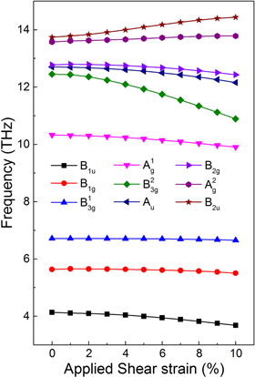
Figure 3. The frequencies of optical modes at the Γ point of phosphorene under applied shear strain.
Download figure:
Standard image High-resolution imageWe have further studied the sound velocities by fitting the slopes of the acoustic dispersion curves around the Γ point. At ambient conditions, our calculated maximum longitudinal velocities of sound along the Γ-to-X direction  = 3.96 km s−1 and along the Γ-to-Y direction
  = 7.99 km s−1, which agree well with previous results by Zhu et al [46]. Herein,
  is about twice as much as
  indicating strong lattice dynamic anisotropy in phosphorene. Figure 4 illustrates the sound velocities as a function of the applied shear strain. Obviously,
  will increase with the increase of the applied shear strain. Meanwhile, the
  will slightly decrease. The maximum velocity of sound along the Γ-to-X direction is
  = 6.81 km s−1, and the Γ-to-Y direction is
  = 7.56 km s−1 under 10% shear strain. As a result, the applied shear strain reduces the strong anisotropy of lattice dynamic properties in phosphorene.

Figure 4. The sound speed of phosphorene as a function of the applied shear strain.
Download figure:
Standard image High-resolution imageThe details of the crystal structure of phosphorene can be found in our previous work [21]. To explore the crystal structure change of phosphorene under shear strains, we plotted the P–P bond length and bond angle as a function of the applied shear strain in figure 5. As can be seen in the figure, the intraplanar P–P bond length R1 will slightly decrease with the increase of the shear strain; the variation of R1 is 0.023 Å from 0–10% shear strain. Meanwhile, 10% shear strain introduces only a 0.002 Å increase for P–P bond length R2. Hence, the P–P bonds show a very tiny response to the shear strain. At the same time, as the shear strain increases, the intraplanar bond angle θ1 keeps its value around 96°, which does not respond to the shear strain as well. While the interplanar angle θ2 drops sharply from 104.18–95.78° under 0–10% shear strains. Hence, the applied shear strain changes the phosphorene lattice by mainly decreasing the interplanar angle θ2.
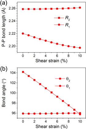
Figure 5. (a) The P–P bond length and (b) bond angle as a function of the applied shear strain.
Download figure:
Standard image High-resolution imagePhosphorene has been predicted to be a nearly direct bandgap semiconductor near the Γ point and can be briefly considered as a direct gap semiconductor [28, 47]. It is well known that PBE usually underestimates the bandgap for semiconductors, while the hybrid functional with the mixing of the Hartree–Fock and DFT exchange energy is a practical method to exactly evaluate the bandgap. Herein, we plotted the bandgap for phosphorene under shear strain both using the PBE and HSE06 methods [39] in figure 6. We have obtained a 1.54 eV bandgap using HSE06 and a 0.91 eV bandgap using PBE for phosphorene. We considered the nearly direct bandgap nature of phosphorene at ambient conditions as the direct gap at Γ. We found that phosphorene keeps the direct bandgap behavior, though its bandgap slightly decreases under no more than 4% applied shear strain, which is similar to the effect of a certain compression strain [29]. By further increasing the applied shear strain, phosphorene will be transformed to an indirect bandgap semiconductor, and the value of the indirect bandgap decreases sharply with the increase of shear strain. As can be seen in figure 6, the HSE06 hybrid functional enlarges the bandgap without any further significant change of the electronic structure, whereas the PBE and HSE06 method represent very similar features and tendencies for the bandgap under shear strain. Hence we will only present the further analysis of the electronic band structure of phosphorene under shear strain based on PBE in the following.
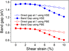
Figure 6. The bandgap of phosphorene as a function of the applied shear strain.
Download figure:
Standard image High-resolution imagePhosphorene shows very strong electronic anisotropy features along the Γ-to-X and Γ-to-Y directions [22]. Figure 5(a) shows the strain-free band structure of phosphorene. Similar to the phonon dispersion curve, the electronic bands along the X-to-M and M-to-Y directions are double degenerated. To further analyze the electronic nature of the direct-to-indirect bandgap transition of phosphorene under shear strain, we plotted the electronic band structure of phosphorene under different shear strains. By comparing the band structures under different shear strains, we found that the shear strain has remarkable effects on the band structure along the X-to-M and M-to-Y directions but not along the Γ-to-X and Γ-to-Y directions. Since the bands along the Γ-to-X and Γ-to-Y directions are very sensitive to the axial strains [29, 30], different behavior of the phosphorene band structure under applied shear strain is expected. As can be seen in figure 7(b), a 1% shear strain splits off all the double- degenerated bands along the X-to-M and M-to-Y directions. At the same time, the double-degenerated states are pinned at the X and Y points. As a result, the corresponding shear strain does not change the electronic features of phosphorene along the Γ-to-X and Γ-to-Y directions. The splitting along the X-to-M and M-to-Y directions increases with the applied shear strain increasing. By increasing the applied shear strain to 5%, the conduction band minimum (CBM) shifts from the pz electron-dominated state at the Γ point to the s electron-dominated state located in the middle of the M-to-Y direction, which comes from the splitting of the s-p hybridized bands [21]. Meanwhile, the valence band maximum (VBM) remains at the Γ point. As a result, phosphorene will transfer from a direct gap semiconductor to an indirect gap semiconductor. Further increasing of the applied shear strain to 10% will not change the indirect bandgap feature. It is worth noting that the s-dominated CBM in the middle of the M-to-Y direction under 5–10% shear strain presents more homogeneous electronic characterizations, which may reduce the anisotropy in phosphorene.

Figure 7. The band structures of phosphorene under (a) 0%, (b) 1%, (c) 5%, and (d) 10% shear strain.
Download figure:
Standard image High-resolution imageTo evaluate the electronic anisotropy in phosphorene under shear strain, we calculated the effective masses of the electron (hole) by fitting the states around the CBM (VBM) [48]. Our calculated effective masses of the electron along the x-direction m*e,x = 0.148 me, and y-direction m*e,y = 1.237 me. Our calculated effective masses of the hole along the x-direction m*h,x = 0.138 me, and y direction m*h,y = 5.917 me. We can define the effective mass anisotropy according to  and
and  For an ideal isotropic electronic system, the values of Ae and Ah equal 1, while any value smaller or greater than 1 is a measure of the degree of electronic structure anisotropy possessed by effective masses along a different direction. Herein, Ae = 8.36 and Ah = 42.88 for phosphorene without any applied shear strain. These results indicate strong electronic anisotropy of phosphorene and agree well with previous studies [22, 29, 30]. Figure 8 illustrates the effective mass of the electron and hole in phosphorene under different applied shear strains. As can be seen, under no more than 4% shear strain, the electron effective mass along the x-direction keeps its value, while the electron effective mass along the y-direction grows with the increasing applied shear strain. Interestingly, the electron effective mass jumps suddenly along the x-direction under 5% applied shear strain, which drops sharply along the y-direction. Such a phenomenon originates from the direct-indirect bandgap transition during the CBM shifting discussed above. As a result, the effective mass anisotropy Ae = 0.41 under 5% applied shear strain, which will further increase to Ae = 0.64 under 10% applied shear strain. On the other hand, there is no VBM shifting during the direct–indirect bandgap transition; hence, the hole effective mass varies gradually. As the shear strain increases, the hole effective mass along the x-direction keeps its value, while the hole effective mass along the y-direction gradually decreases. As a results, the effective mass anisotropy decreases to Ah = 20.41 under 10% applied shear strain. Thus applied shear strain remarkably reduces the electron effective mass anisotropy and partially reduces the hole effective mass anisotropy in phosphorene. Since the carrier mobility is inversely dependent on the effective masses, the carrier mobility anisotropy in phosphorene can be adjusted by applied shear strain as well.
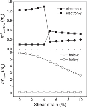
Figure 8. The electron and hole effective mass of phosphorene as a function of the applied shear strain.
Download figure:
Standard image High-resolution imageTo further explore the electronic anisotropy, we studied the decomposed charge density of the CBM of phosphorene. Figure 9(a) plots the isosurface of the decomposed charge density of the Γ point CBM of shear strain-free phosphorene in real space, which is very similar to the previous studies [30]. Continuous electron charge clouds dominate the space above and below the phosphorene layer along the y-direction. On the other hand, discontinuous electronic charge clouds are divided into individual parts along the x-direction inside the phosphorene layer. Hence the CBM of phosphorene shows a strong anisotropy feature. However, according to the CBM shifting during the direct–indirect bandgap transition, the decomposed charge density of the CBM of phosphorene under 5% applied shear strain presents a more homogeneous character, which is shown in figure 9(b). A continuous electron charge along both the x- and y-directions fabricates a 2D charge net inside the phosphorene layer. This result agrees well with our previous analysis about the electron effective mass by fitting the states around the VBM.

Figure 9. The decomposed charge density plots of the conduction band minimum of phosphorene under (a) 0% and (b) 5% shear strain.
Download figure:
Standard image High-resolution image
One of the most important reasons why phosphorene has attracted global interest in potential applications for electronics and optoelectronics is that phosphorene is a direct bandgap semiconductor. Its bandgap, band alignment, and work function can be tuned by changing the sample thickness [22, 49]. Considering that phosphorene can theoretically hold up to 30% critical strain [26], and its physical and chemical properties can be tuned by strain engineering [28, 30], strained phosphorene should be widely used in electronic and optoelectronic devices like strained-silicon MOSFETs [50] in the near future. According to our analysis, there exists a direct-to-indirect bandgap transition in phosphorene under a shear strain as small as 5%. Hence, any form of shear strain, for example, global shear strain, process-induced shear strain, or post-processing shear strain, should be avoided in applications of strained phosphorene. Herein, the anisotropy diminution of phosphorene can be the sign of the appearance of the undesirable shear strain. From another point of view, the electronic anisotropy properties of phosphorene, for instance, the carrier mobility anisotropy, can be adjusted by the shear-induced direct-to-indirect gap transition, which indicates that phosphorene can be applied in potential applications such as a shear strain protecting nanoelectronic switcher.
4. Conclusion
In summary, we have systematically studied phosphorene under applied shear strain based on density functional theory calculations. We found that phosphorene is dynamically stable under no more than 10% applied shear strain. Further analysis of the sound velocities indicates that the applied shear strain reduces the strong anisotropy of lattice dynamic properties in phosphorene. We studied the direct-to-indirect bandgap transition and revealed the related CBM shifting in phosphorene under shear strain. Furthermore, the anisotropy diminution of the electronic structure of phosphorene was explored by investigating the effective mass as well as the decomposed charge density. Our result reveals that strong shear strain should be avoided when designing engineering phosphorene-based electronic or optoelectronic devices. However, phosphorene shows potential application as a nanoelectronic switcher with its shear strain-sensitive anisotropy properties.
Acknowledgments
This work was supported by the National Natural Science Foundation of China (grant nos. 11347007, 61274005, 51301039, and 51171046), the National Natural Science Foundation for Distinguished Young Scientists of China (grant no. 51225205), the Qing Lan Project, and the Priority Academic Program Development of Jiangsu Higher Education Institutions (PAPD).