
Abstract
Is it possible to operate a computing device with zero energy expenditure? This question, once considered just an academic dilemma, has recently become strategic for the future of information and communication technology. In fact, in the last forty years the semiconductor industry has been driven by its ability to scale down the size of the complementary metal-oxide semiconductor-field-effect transistor, the building block of present computing devices, and to increase computing capability density up to a point where the power dissipated in heat during computation has become a serious limitation. To overcome such a limitation, since 2004 the Nanoelectronics Research Initiative has launched a grand challenge to address the fundamental limits of the physics of switches. In Europe, the European Commission has recently funded a set of projects with the aim of minimizing the energy consumption of computing. In this article we briefly review state-of-the-art zero-power computing, with special attention paid to the aspects of energy dissipation at the micro- and nanoscales.
Export citation and abstract BibTeX RIS

Content from this work may be used under the terms of the Creative Commons Attribution 3.0 licence. Any further distribution of this work must maintain attribution to the author(s) and the title of the work, journal citation and DOI.
1. Introduction
In recent years, we have assisted the exponential growth of the information and communication technology (ICT) sector, fostered mainly by the progress made in the semiconductor industry in cost-effectively scaling down the size of solid-state electronic devices. Chief among all of this progress is the decrease in the size of electronic switches (i.e., transistors, complementary metal oxide semiconductor-field-effect transistor (CMOS-FET)4 , which are the building blocks of todayʼs computing devices. This decrease in size has been paralleled by the increase in computing capability due to ever-increasing transistor density, meaning that there is an ever-increasing number of computing elements in each device. However, this increase in density produced an increase in the power of the in heat dissipated during computation, up to the point that this is currently a serious practical limitation [1, 2]. According to the International Technology Roadmap for Semiconductors (ITRS) [3] the limits imposed by the energy dissipated during switch operation will be a roadblock for future scaling over the next 10–15 years. As a consequence, increasing attention has been devoted to the role of energy efficiency in ICT, and a new field called toward zero-power computing has emerged.
The objective of the research in this field covers both scientific and technological aspects. On the scientific side, there is a need to better understand the fundamental physical laws that rule the out-of-equilibrium energy transformation processes at the micro and nanoscales. On the technology side, there is the goal of identifying new solutions for information processing that present improved energy efficiency and allow the continuous growth of computing capabilities.
1.1. Science aspects
The study of energy transformation processes at the micro-and nanoscales raises the problem of evaluating the efficiency of such a transformation. This is a topic that has been the focus of a significant research effort during the foundation of thermodynamics in the 1700s and 1800s. Thanks to the work of scientists like Sadi Carnot and subsequently of Emile Clapeyron, Rudolf Clausius, and William Thomson (Lord Kelvin), studies on the efficiency of machines invented by Thomas Newcomen and James Watt to transform heat into work brought us the notion of entropy and the second law of thermodynamics, which put limits on this efficiency. It is interesting to note that today, 200 years after the work of Carnot, we are still dealing with the problem of defining such limits, although today the object of our interest has moved from the large power plants of the industrial revolution to the tiny devices of modern ICT [4]. It is our understanding that future ICT will be largely affected by nano scale devices that process information while transforming work into heat and heat into work. As a consequence, it seems natural to treat an ICT device as a novel infothermal machine that inputs information and energy (in the form of work), processes both, and outputs information and energy (in the form of heat).
1.2. Technology aspects
On the technology side, other than the urgent objective of reducing the heat produced during computation in high-performance computer systems, there is also another reason why zero-power computing is relevant for ICT. It is associated with the popular concept of ubiquitous computing. The introduction of microelectronic and mechanical systems and nanoelectronic and mechanical systems opened the door to the development of so-called wireless sensors: submillimeter sensors, computers, and actuators that can be interconnected to form a wireless network. These networked devices have wide applications that cover everything from military to civilian applications such as environmental monitoring, biomedical sensing, radio-frequency identification (RFID), interactive control, integrated biology, agriculture, structural monitoring, sensing harmful chemical agents, location of persons, and transportation, just to name a few.
The low-power characteristics of wireless sensor network components and the design of the system architecture are crucial to the longevity of the sensor nodes. The best solution for avoiding the impractical battery-replacement procedure is for each node to be autonomous and self-powered, adsorbing energy from a renewable source that is continuously available in the ambient environment. This approach is called energy harvesting. At present, renewable power can be obtained by generating electrical energy from light, thermal energy, and kinetic energy present within the sensors, environment. The energy from these sources can be used both as a real-time supply for the functioning of the device or can be stored for a later use to augment the battery, thereby increasing the lifetime and capability of the network and mitigating the environmental impact caused by the disposal of batteries. However, before the energy-harvesting technologies become viable solutions, it is necessary to reduce the gap between how much energy can be transformed from the environment in a certain time interval and how much power is required to operate the microdevice. Presently this gap spans about three orders of magnitude (see figure 1), with differences related to different energy-harvesting technologies. For a discussion of these aspects, see [5].
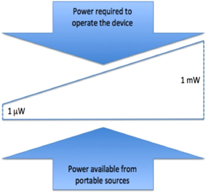
Figure 1. The current gap between how much energy can be transformed from the environment in a certain time interval and how much power is required to operate microelectronic devices. This gap ranges from  to
to  depending on the harvesting technology and the ambient conditions.
Download figure:
Standard image High-resolution imageThe energy consumption of computing technologies not only becomes more and more of an obstacle to realizing new functionalities in, for instance, mobile or distributed applications, and limits high-performance computing, it also has an increasing impact on energy supply and the environment. According to the SMART2020 study [6], Enabling the low carbon economy in the information age, ICTʼs share of global energy consumption is presently in the range of 2–5%. To reach the objective for CO2 emissions targets of at least 20% below 1990 levels in 2020, the SMART2020 report points at the strategic role played by ICT: 'The ICT sectorʼs own emissions are expected to increase, in a business as usual (BAU) scenario, from 0.53 billion tonnes (Gt) carbon dioxide equivalent (CO2e) in 2002 to 1.43 GtCO2e in 2020. But specific ICT opportunities identified in this report can lead to emission reductions five times the size of the sector,s own footprint, up to 7.8 GtCO2e, or 15% of total BAU emissions by 2020'.
As illustrated in figure 2 [7], in modern electronic ICT systems, energy consumption is divided among the four main information processing functions: computation, communication, storage, and display. In the following we focus on the role of computation, being the most basic and omnipresent function in practically all ICT devices.

Figure 2. In modern electronic ICT systems the energy consumption is divided among the four main information processing functions: computation, communication, storage, and display.
Download figure:
Standard image High-resolution image2. Energy dissipation in existing nanoelectronic switches
The energetics of computation has attracted much interest in recent years due to the potential impact of this issue on the development of ICT. As we briefly mentioned in the introduction, the power dissipated during computation is a serious limit to the further increases in transistor density. Since 2004, the Nanoelectronics Research Initiative5 , a US-based consortium of Semiconductor Industry Association companies, has launched a grand challenge to address the fundamental limits of the physics of logic switches, the basic element of the modern computer. Such an initiative has been somehow paralleled in Europe by Aeneas6 with the so-called More than Moore approach and recently with the FET Proactive initiative denominated MINECC (Minimizing Energy Consumption of Computing to the Limit)7 .
The information developed in this framework focused mainly on the operation of an FET transistor, which is used here as a logic switch. The progressive miniaturization of FET transistors has permitted larger and larger densities, up to the point that the present generation of commercial microprocessors presents a density as high as 2 billion transistors per square centimeter [8]. Such a high transistor density of transistors is responsible for the phenomenon of device heating, which is presently the main technological limitation to a further increase in transistor density. In fact, in todayʼs microprocessors the power dissipated in heat is close to  . It has been estimated that if the transistor density is exploited to the physical limits, the resulting power density for these switches at maximum packing density would be on the order of
  which is orders of magnitude higher than the practical air-cooling limit [2].
To better understand where and when the energy gets dissipated during computation we need to consider that the figures we discussed above are specific to existing electronic technology, called CMOS, and that they are mainly due to the peculiar operation procedure assumed in the functioning of the transistor itself. In fact, the main sources of energy consumption in electronics are the charging and discharging of electrical capacitances, which are present in all electronic devices and are associated with the functioning of the transistor as a logic switch. By assembling logic switches, we can build logic gates and memory devices and use them to perform all the logic and arithmetic operations required. Logic switches can also be used as a building block of memory devices.
In figure 3 we show an possible configuration where an FET is coupled to an external capacitor to form a dynamic random-access memory device. In this case, in addition to the gate capacitance Cg, of the FET and the interconnection capacitance, Ci, arising from the connection between different devices, figure 3 also shows the capacitance due to the storace capacitor, Cs. During the switch operation in an FET transistor, the capacitor is charged/discharged from/to a constant voltage power supply. This produces a total energy dissipated (i.e., converted into heat), per cycle, in the measure of [9]:

where V is the voltage of the power supply. If the switching operation is performed with frequency f, then the power dissipated is:

where α is the activity factor ( , for a square-wave switching). Psw is usually called the dynamic switching power and is directly associated with on/off switching (usually, in ordinary devices, there is also a parasitic leakage power component that adds to dissipation). In the last 40 years dynamic switching power has been constantly reduced as a result of scaling down the devices' critical dimension, d, from micrometers to nanometers. Such scaling has produced a proportional decrease in the device capacitance, Cg. The voltage, V, underwent a similar scaling down proportional to d. This situation has produced a progressive decrease in the dynamic switching power that is approximately proportional to d3, a behavior confirmed by data obtained form several editions of the ITRS [3] and illustrated in [9].
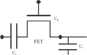
Figure 3. Example of a dynamic random-access memory (DRAM) where several distinct capacitors are present: the gate capacitance, Cg, of the FET; the interconnection capacitance, Ci, arising from the connection between different devices; the capacitance, Cs, that results from to the storace capacitor.
Download figure:
Standard image High-resolution imageIt is interesting to note that while for devices with  the switching energy of the transistor is the dominant factor in the total chip energy consumption, for sub-
 technology nodes, the fraction of the transistor dynamic energy in the energy balance decreases. Indeed, transistor dynamic energy consumption constitutes
  of the total energy in modern microprocessors (
 node), and is expected to further decrease for
  devices and below [9]. This is mainly due to the increasingly important role of dissipation in interconnects and off-state leakage losses. The state-of-the-art switching energies with FET transistors are currently on the order of a few
  .
.
In figure 4 we present the impressive decrease in energy consumption in switch devices used over computation in the last 80 years.

Figure 4. Switch energy in J versus time. After [10].
Download figure:
Standard image High-resolution imageDue to the important role of switches in the future of ICT, it is relevant to address the following question: Is there any fundamental physical limit to the minimum energy required to operate a switch? Surprisingly enough, there is no general agreement on the answer to this question in the physics/technology community. To determine the correct answer to this question, we need to introduce a certain degree of abstraction to the treatment of the switch device. Let's start by considering the role of a switch in a generic computation process. We can think of a switch as a generic physical system characterized by (at least) two stable states. Under the action of an external force, the system can change its state by switching from one state to the other. In figure 5 we present a schematic representation of a switch device where the external force is considered as input and the state (open or closed) is the output. In the electronic (or electro mechanical) realization of the switch, the status is represented by the value of an electrical current or an electrical voltage that changes as a consequence of the change in the state of the switch.
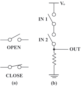
Figure 5. Switch operation. (a) The two states of a switch: open and closed. (b) A set of two switches arranged to realize an 'and' gate in the electronic standard configuration. When the inputs produce the state 'closed' in both the switches, the voltage at the 'out' point assume, the value  . Otherwise, it is zero.
Download figure:
Standard image High-resolution imageIn this framework, a computation is performed every time time a switch changes its status. Clearly by combining switches we can realize logic gates (and thus logic gate networks), memory devices, and perform all the computation required for a given task.
Letʼs consider the potential energy that regulates the functioning of a switch, represented in figure 6. The two logic states, 0 and 1, are here represented by a material particle (an electron or the equivalent information carrier) sitting in the left and right well, respectively. The switching event is obtained by making the particle energetic enough to overcome the potential barrier separating the two states or, equivalently, by lowering the potential barrier on the particle side. Notwithstanding the simplicity of this model, it has often been applied [2] to estimate the relevant aspects of the physics of switches. Specifically, the minimum operational energy of the switch is computed by assuming that the barrier height, Eb, is large enough to enable the distinguishability of the two logic states. Such a condition is, in fact, threatened by unwanted crossings of the potential barrier due to thermally induced (classical) jumps or tunneling (quantum) effects. The larger Eb and the distance between the two wells, the lower the threat to the distinguishability of the two states. Additionally, the Heisenberg energy-time uncertainty relation is invoked in this context to set a further limit to the barrier height, Eb. Based on these arguments, Cavin et al were able to estimate a minimum energy per switching event of approximately  .
.

Figure 6. Bistable potential energy, U(x). The two states of a switch (open and closed) are here represented as logic state 0, 1, associated with  ,
,  . To be dynamically stable, the two states are separated by a potential energy barrier, Eb.
Download figure:
Standard image High-resolution image3. The physics of nanoscale switches
To continue in the search for the minimum energy required to operate a switch, we should introduce a general dynamical model that is capable of representing the main features of a physical switch like the one we have just described without being limited by the considerations associated with the peculiarities of the electric charge dynamics. Thus we propose to discuss the switch dynamics in terms of the continuous dynamics of a single degree of freedom, x(t), ideally representing a relevant observable of the switch dynamics (e.g., the position of a material particle or of a cursor and the quantity of electric charge or the value of magnetic or electric field). To represent the binary character of the switch, we need to identify the two logic states: we assume that the logic state 0 (1) is associated with  (
( ). As we mentioned previously, the two states have to be dynamically stable and thus are separated by a potential energy barrier, Eb. Taking into account the physical character of a generic small-scale binary switch, we imagine it to be in contact with a thermal bath at a constant temperature, T.
The continuous dynamics of x(t) can be mathematically described by a proper Langevin equation [11]:

where  is a symmetric stationary bistable potential and
  is an external force that can be applied to change the logic state.
  is the time-evolving potential energy landscape and
  is the total conservative force acting on the system.
  represents the fluctuating force whose statistical features are connected with the dissipative properties, γ, by a proper fluctuation-dissipation relation [12]. The time evolution of the corresponding probability density,
  is usually described in terms of the associated Fokker–Planck equation [11]. The two states, 0 and 1, are realized with the respective probablities p0 and p1 (
 ), given by:

States 0 and 1 have the same energy thanks to potential symmetry, so to perform the switch operation with zero energy expenditure, we need to reduce to zero the work performed by the deterministic forces acting on the system. The deterministic forces are represented here by the conservative force  and the dissipative force
  . In the following, we exclude the case of a reversible transformation where the work performed against the conservative forces during the switch is stored as potential energy in some external place and recovered subsequently, because this condition is practically difficult to implement in a small-scale switch.
To begin our analysis, let's start with the following procedure (see the left-hand side of figure 7, standard procedure) [13], which presents a switch from 0 to 1 (the 1 to 0 switching is analogous). We start with the system in the logic state, 0 (step 1: first picture from the top). Here the potential barrier, Eb, is initially lowered to zero (step 2), and subsequently the potential is tilted in order to move the particle to the right well (step 3). Finally, the barrier is raised to its initial value (step 4) and the tilt is removed (step 5). All five steps in this procedure can be performed by a proper application of the external force,  in order to keep the average velocity of the particle close to zero (zero friction) and the average position in correspondence to an approximately zero derivative potential value (zero deterministic force). However, in spite of negligible friction and negligible external work performed on the system, this procedure does not allow for a zero-power switching. This is due to the unavoidable entropy reduction occurring in steps 3–5, after its sudden increase in steps 1 and 2, due to the barrier drop. This is apparent from the change in the probability distribution (see figure 7, left) and can be demonstrated quantitatively as follows. The system entropy in the various steps can be computed according to Gibbs as:

where we assume that the Gibbs entropy and the Shannon entropy coincide [19].  indicates the step number and i = 0,1. In step 1, we have
  and
and  ,
,  . In step 2,
  and thus
  . Therefore, the change in entropy is
  . On the other hand, from steps 3–5, entropy is reduced from S2 to
  , thus
  . According to the thermodynamics, while the entropy increase can be performed without energy exchange, these last steps cannot be performed without energy expenditure. This result is also in agreement with what has been observed in the simulation of a nano-magnetic system [14] where this switch procedure has been applied.
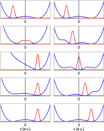
Figure 7. Schematic representation of a switching procedure. Left:  . Changes in the probability distribution (red) and in the potential U(x) (blue) due to the application of the external force, f(t). Steps 1 to 5, from top to bottom. Right:
  . To satisfy conditions 1 and 2, we slowly apply a proper external force, f(t), that always keeps the average position of the particle close to the minimum of the potential well and does not change the probability density along the path (cond. 3), in a constant entropy transformation condition.
Download figure:
Standard image High-resolution imageThus, based on this discussion, we are now in a position to answer the question that was posed at the beginning of this section. The minimum energy required to operate a switch is zero, provided that the following conditions are obeyed: (1) The application of the external force always keeps the average position of the particle close to the minimum of the potential well (zero total force). (2) The switch event has to proceed with as small a speed as possible (zero friction approximation). (3) The system entropy must remain constant during the switch event. The right-hand side of figure 7 shows an example of a possible procedure that satisfies these three conditions.
4. Nanomagnetic zero-power switches
To test these conclusions, a prototype nanoscale switch has been considered in the form of a single cylindrical element of permalloy (NiFe) with dimensions  nm3 discretized in elementary cells of
  nm3 Micromagnetic simulations of the switch dynamics have been performed at T = 300 K, and the effect of thermal fluctuations is introduced into the simulation with a random fluctuating magnetic field, which is delta correlated both in time and in space, with an amplitude that fulfils the fluctuation-dissipation theorem [15].
To simulate a bistable system, we introduced a uniaxial anisotropy in the plane of the NiFe dot, along the y-direction. This anisotropy defines two low-energy states for the magnetization,  and
and  , which can be defined as 0 and 1 states, respectively. These two energy minima are separated by an energy barrier whose height is determined by the value of the uniaxial anisotropy constant, K1.
The switching procedure was realized by applying a sequence of external magnetic fields, which is illustrated in the upper part of figure 8. (This procedure was inspired by the zero-power procedure previously described.) The presence of the uniaxial anisotropy along the y-direction is represented in the figure using an elliptical shape with its major axis parallel to y. The system starts within no applied external field and with the initial magnetization oriented along the positive y-direction (i.e., the system is in one of the two energy minima). In the first stage, a positive external field (H) is applied along y with a slope, up to a maximum value of H = 1.0 kOe. After that, the external field is slowly rotated in the  plane of 180o toward the negative y-direction, keeping its amplitude fixed at the value H = 1.0 kOe. During the final stage of the simulation, the external field is removed with a negative slope, opposite to that of the first stage. The energy dissipated during the switching procedure is then calculated as the integral of the scalar product
  where
where  is the average magnetization of the system. The total switch time was also varied in the range
  ns. The results shown in figure 8 (lower) for the micromagnetic simulations represent the energy dissipation during the switching procedure as a function of the total switch time. The calculations were performed for a barrier height of about 40 kBT. In this switching procedure, the external field is applied parallel to the initial magnetization configuration so the system remains in the absolute minimum energy state during the whole procedure. For comparison, the same figure also shows the results obtained with the numerical solution of equation (1) [20].

Figure 8. Upper: five steps of the zero-power procedure (process A) applied to the magnetic dot. Lower: energy dissipated during the zero-power switching procedure versus overall switch time. Results from micromagnetic simulations (red) and digital simulation of equation (3) (with  Kg,
Kg,  Kg
Kg  ,
,  ) (blue). Micro magnetic simulations have been realized with a customized version of Micromagus commercial software. Magnetic parameters have standard values for bulk permalloy: saturation magnetization
 , exchange stiffness constant
 , damping coefficient
  and
and  .
.
Download figure:
Standard image High-resolution imageFigure 8 are also shows the results obtained with Euler–Maruyama integration of equation (3) with  Kg,
Kg,  Kg
Kg  ,
,  .
.  is an uncorrelated white noise, so its cumulants satisfy
  and
and  .
.  with
with 
 and
and 
 ;
;  then has two minima in
 separated by an energy barrier,
  . These choices are consistent with the dynamics of a one-dimentional micrometric bead dispersed in distilled water [13].We assume that at t = 0, the bead is in local equilibrium within the left well of
  . To perform a zero-power switching, we then apply, for a time span of length τ, an additional
  such that the total potential energy
  is a time-variable ninth-order polynomial. For large values of τ,
  gives one analytical representation of the zero power protocol shown in figure 7 (right). The average heat exchanged by the particle with the thermal bath is computed as the Stratonovic integral [20]
where the angle brackets stand for the average over many simulated trajectories.
Both sets of data clearly show that the dissipated energy can be made as small as needed by increasing the total switch procedure duration, asymptotically reaching the zero energy dissipation limit, according to our prediction. Based on these considerations for the zero-power switching, we can critically address the recent observation [21] that in order to reach zero-power switch operation, a key element is represented by the existence of a copy of the switch already in the final destination status. We have shown here that this condition is not required in a binary switch. Moreover, we want to stress that the switch operation realized here is performed according to the leads discussed in the previous paragraph. Thus the transformation is reversible and does not decrease entropy. In the next section, we will consider a transformation where irreversibility via a net decrease of entropy arises: the so-called Landauer reset.
5. Switch versus reset operation: the Landauer limit
In the dynamical description provided above (see (3)), we assumed that due to the coupling with the thermal bath, a fluctuating force,  appears. At thermal equilibrium, the fluctuation-dissipation theorem, [12] links
  and the dissipative force, γ. In a generic computing device, the practical switch is supposed to rest in one of the two logic states between two subsequent switching procedures. In a nanoscale switch, the role of fluctuations cannot be neglected, and thus in our bistable model, due to the presence of the fluctuating force, the particle will oscillate around the potential minima, with occasional random crossings of the potential barrier between the two wells. More specifically, if we place the particle at rest at the bottom of the left well, it starts to oscillate, and after some time,
  it reaches a constant oscillation amplitude. If we wait long enough we can observe that after a time,
  it will jump into the right well and eventually back into the left well, and so on at a constant pace.
  and
and  are random variables whose average values are usually referred to as intrawell relaxation time and the the interwell relaxation time, respectively. They represent the average time the system takes to establish local equilibrium within one well (as it would be if the potential was no wider than a single well) and the average time it takes to go to global equilibrium in the entire potential, respectively. By the moment that
  depends exponentially on the barrier height between the two wells, in practical switches, the barrier height is chosen to be large enough to guarantee
  .
.
In the description of the switch event, we implicitly assumed that the system is at local equilibrium in a given well and that the switching process proceeds within a time,  such that
  . Now let's suppose that instead, we are not at local equilibrium anymore but rather have reached a global equilibrium, (i.e., before starting the switch process, we have waited a time,
  ).
).
Since the potential is symmetrical and the fluctuating force has zero average, the two states, 0 and 1, have the same probability. This implies that the probability density distribution at equilibrium  is stationary and symmetric, as represented in figure 9. Here,
  .
.
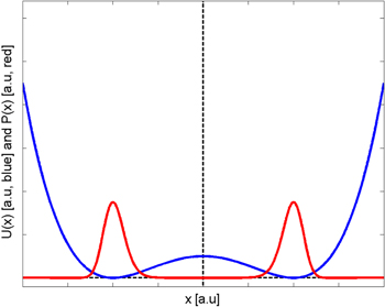
Figure 9. Potential energy U(x) (blue) and equilibrium probability density  (red).
Download figure:
Standard image High-resolution imageIf we want to perform a switch operation, say 0 to 1 we need to operate a transformation that changes, the probability density distribution in order to reach the condition  ,
,  . This transformation is usually called the reset. From this perspective, we can say that a switch operation transforms a local equilibrium condition into another local equilibrium condition, while a reset operation transforms a global equilibrium condition into a local equilibrium condition.
Similarly to what we have done for the switch operations, we can identify a proper procedure that minimize, the energy required to operate the reset by zeroing the work done by the deterministic forces. In this case, however, the resulting change in entropy cannot be made null. In fact, in the initial state we have  and
and  ,
,  while in the final state we have
  and
and  , Sf = 0. Thus the change in entropy is
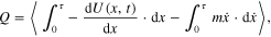
  . According to the second principle of thermodynamics, this amounts to a minimum energy, Q, to be dissipated:

where T is the temperature. This result, often called the Landauer principle, represents a version of the second principle of thermodynamics that, assuming the Shannon information as a special form of the Gibbs–Boltzmann entropy, establishes that a necessary condition to operate a computing device with zero energy dissipated is that the computing process does not decrease information [16–19]. It has recently been experimentally tested [13, 21, 22], with the aim of exploring the limits in low-power computation [14].
6. Operating nanoscale switches in the presence of fluctuations
When we operate the binary switch device in the presence of fluctuations—a condition that is typical in the case of nanoscale switches—we are faced with the problem of unwanted barrier-crossing events. In fact, even if we set our barrier high enough that our resulting  , there is always a finite probability that a jump occurs. The effect of these random crossings is interpreted as a switch error that produces a logical bit flip. Bit flips occur with a certain probability in any real switch, as a result of fluctuations in the presence of a finite barrier height [23]. In this section, we explore the role of bit-flip errors in determining the minimum energy.
6.1. Energy versus error in the reset operation
Let's start with the reset operation. Let's suppose that during the reset to 0 operation, a bit flip occurs with a certain probability,  . As a result of the reset error, a finite probability, p1, appears. In figure 10, we present the probability densities before and after the reset to 0.

Figure 10. Potential energy and probability density function. (a) The probability density function p(x) is plotted together with the potential energy for the symmetric case. The probability of realization of a given logic state is represented by the shaded area below p(x), for 0 (left well) and for 1 (right well). (b) Same quantities as in (a), after the reset operation. The area under the right side can be interpreted as the error probability Pe.
Download figure:
Standard image High-resolution imageTo compute the minimum energy, let's proceed with the computation of the entropy change. The Gibbs entropy before the reset operation  is promptly computed as
  . After the reset operation, we have:

where we used  . Accordingly, the energy dissipated during the erasure operation is now a function of the error probability:
  —that is,

In figure 11, we plot the energy ratio  as a function of the error probability, Pe. As one can see, for
  we have
  , implying that if we are willing to accept a larger-than-zero error probability, we can beat the Landauer limit and perform the resetting operation with an energy toll smaller than
  . Consistently, the zero limit for energy dissipation is reached when Pe = 0.5, corresponding to the maximum uncertainty (complete undistinguishability) (i.e., no reset). In the Pe = 0 limit, we regain the Landauer's prediction,
  .
.
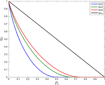
Figure 11. Energy ratio  as a function of the error probability, Pe. The energy ratio,
  represents the fraction of Landauer's energy required to perform the reset operation in the presence of a finite error probability, Pe. For a bistable latch
  if we accept an error probability of 20%
  we need to dissipate approx
  of the minimum required by the Landauer limit. Multistable devices
  show an energy ratio,
  larger than the bistable one. In the large N limit,
  becomes a linear function of Pe.
Download figure:
Standard image High-resolution image6.2. Energy versus error in the switch operation
Let's consider the switch operation. We have already demonstrated that if we apply the zero-power procedure, we can perform the switch with zero energy expenditure. Now let's consider the case in which we apply the 0-to-1 switch procedure when the state of the system, instead of being in the proper 0 initial state, is already in 1 state as a result of a bit-flip error. In this case, what we can demonstrate is that if after the procedure the final state is still 1, then the minimum energy cost of this operation is  .
.
This is easily demonstrated by assuming that we want to use this procedure for resetting to 1. We can compute the energy dissipated as the sum of two processes that are realized with probability  each: the switch 0-to-1 with energy QA and the transformation 1-to-1 with energy QB. Due to the Landauer principle, the total energy dissipated is
  . However, in hypothesis it was QA = 0 (because the minimum energy of this switch can be zero with a zero-power procedure); thus
  .
.
In figure 12 we show the results of the digital simulation of equation (3), together with the micromagnetic simulations, as before. In this set of simulations, however, the initial magnetization of the system was set to be antiparallel to the applied external field, realizing process B. Here the system starts on a relative energy minimum, which becomes more and more unstable as the external magnetic field is increased in the opposite direction, until the magnetization is forced to reverse toward the absolute minimum energy state. Simulations show that the energy dissipated is much larger with respect to the process A, and it can be reduced toward the limit,  while reducing the energy barrier height.
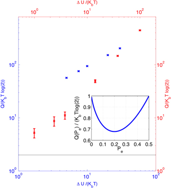
Figure 12. Energy dissipated during the zero-power switching procedure, process B, versus barrier height. Results from micro-magnetic simulations (red) and digital simulation of equation (3) (blue). The horizontal line represents the minimum energy toll at  . (inset) Minimum energy
  as a function of the error probability Pe.
Download figure:
Standard image High-resolution image
As we have anticipated, as a consequence of a bit-flip error, the switch is assumed to be in the wrong logical status; thus when we apply the proper zero-power procedure, we incur a minimum energy toll of  , as just demonstrated. This argument is reminiscent of the minimum energy toll required when operating the electronic switches [2] but in contrast, this is of a fundamental nature and applies regardless to the technology employed of build the switch.
We observe that this result poses a limit to the trading between energy and uncertainty [24] in the reset operation we discussed above. As was observed [24], the Landauer limit can be beaten by accepting a finite error probability, Pe, during the reset. However, such a gain is now balanced by the additional energy dissipation due to the switch error condition that affects the subsequent switch. By putting together the two contributions, we can determine the minimum energy associated with the sequence reset-and-switch as a function of the reset error probability. The relation that generalizes the one obtained in [24] is expressed by 

 .
.
In figure 12 (inset) we plot the minimum energy,  as a function of the error probability, Pe. Remarkably,
  shows a minimum
  , for
, for  independent from T. Such a behavior, characterized by the existence of an optimal error probability (e.g., due to a given noise intensity) that minimizes the reset-and-switch energy is reminiscent of a vast class of phenomena where the presence of a finite amount of fluctuations, instead of being detrimental, is actually beneficial [25].
7. Conclusions
We started this review by asking a provocative question: is it possible to operate a computing device with zero energy expenditure? Our question was motivated by the technological need to reduce the amount of energy currently dissipated during computation. To provide a meaningful answer, we addressed the most basic component of todayʼs computing devices: the logic switches. Based on our analysis of the physics of a general dynamical model of the switch, we concluded that, provided a proper switch protocol is applied, there is no lower bound to the minimum energy required to operate the switch. This result was tested with dynamical simulations of a nano-magnetic switch prototype. Further considerations on the functioning of the nano switches in the presence of large fluctuations have elucidated the role of noise-induced errors in switching energetics.
Acknowledgments
The authors gratefully acknowledge financial support from the European Commission (FPVII, Grant agreement no: 318287, LANDAUER and Grant agreement no: 611004, ICT-Energy), Fondazione Cassa di Risparmio di Perugia (Bando a tema Ricerca di Base 2013, Caratterizzazione e micro-caratterizzazione di circuiti MEMS per generazione di energia pulita) and ONRG grant N00014-11-1-0695.
Footnotes
- 4
CMOS (Complementary MetalOxideSemiconductor), FET (Field-Effect Transistor)
- 5
The Nanoelectronics Research Initiative (nri.src.org) was formed in 2004 as a consortium of Semiconductor Industry Association (SIA) (www.siaonline.org) companies to manage a university-based research program as part of the Semiconductor Research Corporation (SRC) (www.src.org)
- 6
A ENEAS is a non-profit industrial association established under French law, continuing the activities of the former ENIAC Platform and representing the Nanoelectronics partners in the Joint Undertaking in Europe.
- 7
Minimising Energy Consumption of Computing to the Limit (MINECC) is a FET Proactive initiative http://cordis.europa.eu/fp7/ict/fet-proactive/minecc_en.html