

Abstract
The use of electron and ion beam deposition to make devices containing discrete nanostructures as interconnectors is a well-known nanofabrication process. Classically, one-dimensional materials such as carbon nanotubes (CNTs) have been electrically characterized by resorting to these beam deposition methods. While much attention has been given to the interconnectors, less is known about the contacting electrodes (or leads). In particular, the structure and chemistry of the electrode–interconnector interface is a topic that deserves more attention, as it is critical to understand the device behavior. Here, the structure and chemistry of Pt electrodes, deposited either with electron or ion beams and contacted to a CNT, are analyzed before and after thermally annealing the device in a vacuum. Free-standing Pt nanorods, acting as beam-deposited electrode models, are also characterized pre- and post-annealing. Overall, the as-deposited leads contain a non-negligible amount of amorphous carbon that is consolidated, upon heating, as a partially graphitized outer shell enveloping a Pt core. This observation raises pertinent questions regarding the definition of electrode–nanostructure interfaces in electrical devices, in particular long-standing assumptions of metal-CNT contacts fabricated by direct beam deposition methods.
Export citation and abstract BibTeX RIS
1. Introduction
Nanostructured materials have been studied extensively in the last few decades for applications in nanoscaled electronics [1–3]. For this purpose, electrical transport studies are generally performed by depositing metal electrodes using various nanofabrication methods. One of the most common is electron beam lithography (EBL) given its similarities with photolithography. However, EBL requires long processing times along with several fabrication steps (exposure, development, lift-off) [4]. Alternatively, direct deposition methods such as ion beam induced deposition (IBID) and electron beam induced deposition (EBID) are growing in popularity as they allow the preparation of nanodevices with minimum delay and fewer processing steps. Moreover, they offer higher flexibility for fabrication of complex structures and, theoretically, no limits for depositing any metal. Compared to EBL devices, contact resistance values of as-deposited IBID are lower or within the same range [5]. That changes for as-deposited EBID structures because of the higher content of amorphous carbon. The carbon originates from the organometallic molecular precursors used both in IBID and EBID, as these dissociate into the volatile (hydrocarbon) and non-volatile (metal) parts upon deposition. Given the dielectric nature of amorphous carbon, post-fabrication processes have been employed to improve the conductivity of as-deposited EBID structures [6–8]. With annealing, for instance, the size of the beam-deposited metal nanoparticles increases and the amorphous carbon is either crystallized or removed from the structure [9]. In most cases, an oxygen atmosphere is used to etch the amorphous carbon matrix [9, 10]. Unfortunately, this process may result in the onset of structural voids and it is not applicable to carbon-based devices [10].
As early as 1996, IBID of W was employed in electrical transport studies of discrete CNTs [11]. Since then, many other teams have used IBID and EBID to characterize nanocarbons [5]. Generally, studies focus on analyzing the electrical transport properties of the carbon nanostructure and provide limited information on the nature of the contacts or the steps and parameters that are required to optimize the device. In fact, the study of the electrode–nanocarbon interface to improve transport across the contact is a central issue [12]. One strategy to maximize the metal–carbon interaction is to deposit films of a-C by EBID [13] and to thermally anneal the device [14]. Expected structural rearrangements on the a-C and metal leads can be investigated by electron microscopy using free-standing EBID nanorods [15]. Overall, there is still insufficient insight into the structure and chemistry of beam-deposited metal electrodes and how these evolve with post-fabrication treatment.
In this study, the Pt electrodes of CNT devices fabricated with IBID or EBID are studied pre- and post-thermal annealing in a vacuum. Four-probe electrical characterization is performed and complemented by the structural and chemical analysis of both complete devices and analogous free-standing nanorods.
2. Results and discussion
2.1. Carbon nanotubes
The 4''-wafer received from AIXTRON Ltd was fully covered with a dense mat of multi-wall CNTs (MWCNTs). First, a piece of it was cut to carry out cross-sectional imaging with scanning electron microscopy (SEM). Figure 1(a) shows that the MWCNTs were straight, vertically well-aligned and had fairly uniform height (10–12 μm). The tips of the nanotubes commonly presented catalyst particles (inset of figure 1(a)). These were chemically analyzed with EDX, confirming their Ni composition. The internal microstructure of the nanotubes was analyzed with TEM (figure 1(b)) revealing a bamboo-type arrangement with a high density of structural defects and layers transversal to the major axis. The range of diameters for the inner and outer shells was 50–70 nm and 80–120 nm, respectively. Further characterization was performed with Raman spectroscopy. The spectrum in figure 1(c) shows the bands associated with the presence of Si (substrate) and C (MWCNT). In the inset of figure 1(c), the region of 1000–2000 cm−1 is highlighted to show the denominated D (1360 cm−1) and G (1593 cm−1) bands. Despite the overlap, a Gaussian deconvolution shows an intensity ratio, ID/IG, of 0.92, thereby confirming the generalized presence of structural defects in the carbon lattice. These nanotubes could be extracted from the Si wafer and dispersed in an organic solvent to bear discrete nanostructures for subsequent device fabrication.
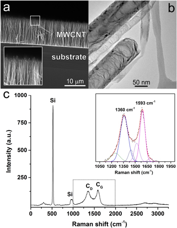
Figure 1. Structural characterization of vertically-aligned MWCNTs grown on a 4'' SiO2/Si wafer. (a) SEM image of a 12 μm high nanotube forest; inset: detail of the boxed area showing the ends of the nanotubes. (b) TEM micrograph illustrating the internal structure of the MWCNTs. (c) Raman spectrum of the nanotubes–substrate ensemble; inset: detail of (c) highlighting the carbon D and G bands and respective peak fitting.
Download figure:
Standard image High-resolution image2.2. Device fabrication, processing and characterization
For both IBID and EBID, preliminary dose tests were performed in preparation for the device fabrication. Specifically for IBID, the beam current was altered at a fixed accelerating voltage to find the point when the deposition rate was faster than the sputtering. A balance was also achieved to minimize contamination in the nanotube (e.g. implantation) and leakage currents (e.g. secondary deposition). Two- and four-probe IBID and EBID blank devices were also constructed and processed to test the Pt deposited structures (i.e. shorted devices). The devices were then subjected to prolonged vacuum annealing (1 h, P = 10 mbar) at 100 °C, 200 °C and 300 °C. It was found that the optimized electrical conductivity was achieved at 300 °C, with few gains possible beyond this temperature. These blank systems were characterized structurally and chemically, pre- and post-annealing, and provided important background insight on the electrical behavior for the analogous nanotube devices. More information on this can be found in the supporting information (available at stacks.iop.org/NANO/26/445301/mmedia).
2.2.1. IBID devices
Four-probe devices connecting a discrete MWCNT were made via the deposition of Pt, as shown in figure 2(a). The electrical characterization showed an initial linear I–V relation indicating an Ohmic-like behavior at room temperature (figure 2(b)). Seven devices were made and tested. In average, the electrical resistance of the as-deposited devices was 60.7 kΩ (in two probes configuration) with a calculated contact resistance of 6.2 kΩ (table 1). Upon vacuum annealing vacuum at 300 °C, a lower device resistance is observed (49.5 kΩ) while the contact resistance remains practically constant 6.0 kΩ. Likely, the better conductance originates from the depletion of Ga that may have been non-intentionally integrated in the nanotube lattice and/or structural rearrangements in the CNT interconnect. Overall, the resistance of the MWCNTs after annealing is in the interval 1 to 10 kΩ. These values are in the same range of analogous arc-discharge CNT IBID devices reported previously [16, 17] (these nanotubes are known to have better structural ordering than chemical vapor deposition, CVD, ones). One additional point worth mentioning is the consistency of our measured CNT resistances. Whereas in other reports these varied by as much as six orders of magnitude [11], in the present case the spread was limited to a tenfold difference. Taken together, the values and relative uniformity of resistances attest to both the effectiveness of our annealing procedure and the similarity of electronic properties of the CVD nanotubes we used.
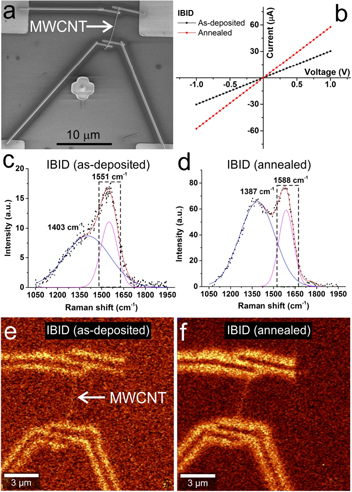
Figure 2. IBID Pt device characterization. (a) SEM image of the as-deposited device. (b) I–V plots of the device in (a) before (in black) and after (in red) annealing. (c) Detail of the Raman spectrum, taken from the as-deposited Pt electrodes, and deconvolution of the overlapping carbon D and G bands. (d) Deconvolution of the overlapping carbon D and G bands taken after device annealing at 300 °C in a vacuum. (e) Carbon G band mapping of a four-probe nanotube as-deposited device on a SiO2/Si substrate. (f) G band map of the device after annealing. The maps in (e) and (f) were drawn using the energy window marked in (c) and (d), respectively.
Download figure:
Standard image High-resolution imageTable 1. Average (N ≥ 7) two-probe resistance (R) values, with respective standard deviations in parentheses, for beam-deposited devices; average contact resistance (Rcont) values and associated standard deviations.
| Device-type | As-deposited [kΩ] | Annealed [kΩ] |
|---|---|---|
| IBID | R = 60.7(±39.0) | R = 49.5(±33.5) |
| Rcont = 6.2(±2.2) | Rcont = 6.0(±1.7) | |
| EBID | R = 7(±4) × 104 | R = 18.0(±6.1) |
| Rcont = 3(±1) × 104 | Rcont = 1.0(±0.2) |
In addition to electrical probing, the structure and chemistry of the IBID devices were analyzed. A first study with SEM did not reveal changes from the pre- to the post-annealed states of the device. Often, such an observation has led to the assumption that the electrodes are stable upon annealing and any changes to contact resistance are due to rearrangements at the electrode–interconnect interface. As we show next, this notion is incomplete.
Following the SEM analysis, the surface topography, width and height profiles of the IBID electrodes, pre- and post-annealing, were investigated with atomic force microscopy (AFM) (supporting information, figure S5). The as-deposited Pt leads had a width of 400 nm and height of 120 nm. After annealing, both surface and dimensions remained practically constant. Raman studies were also performed. Figure 2(c) shows a typical spectrum in the 1000–2000 cm−1 region taken for an as-deposited electrode. The overlap of the D and G bands is notorious with the characteristics of each of these bands (as per the Gaussian peak fitting) described in table 2. Upon annealing (figure 2(d)), the D band shifts to lower wavenumbers and becomes narrower. For the G band, while also narrowing, the shift occurs in the opposite direction with an increase of more than 30 cm−1. As regards the intensity ratio of these bands (ID/IG), this increases from 0.80 to 1.11. These observations indicate that the carbon structure changed considerably with the annealing treatment. On its own, the increased ID/IG ratio is misleading as it may lead to a conclusion that there was amorphization of the structure. In fact, as the deconvolution shows, the broader D band is responsible for the relatively higher intensity of the G band in the as-deposited configuration. Upon annealing, the overlap is no longer as strong and justifies the decrease in intensity of the G band. The narrowing of the bands, together with the wider separation of their maximums, point to a carbon lattice rearrangement, possibly accompanied by increased structural ordering [18]. In the specific case of IBID, the Ga metal contaminant should be removed upon annealing (melting point of ∼30 °C) [19], further helping in the structural rearrangement. Figures 2(e) and (f) show G band Raman maps taken from a 150 cm−1 wide window (marked in figures 2(c) and (d)). In the as-deposited device map (figure 2(e)), it is possible to identify the relatively weak signal of the nanotube connecting the four electrodes as well as the carbon footprint of the latter. The carbon distribution is quite remarkable as it reveals an intense concentration at the edges of the electrodes, thereby signaling a core–shell type structure. This carbon shell becomes more noticeable in the annealed device, consistent with the presence of a thicker coating.
Table 2. Raman shifts of characteristic C bands in Pt electrodes.
| Device | D banda [cm−1] | G banda [cm−1] | ID/IG |
|---|---|---|---|
| IBID | 1403 | 1551 | 0.80 |
| (as-deposited) | (355) | (155) | |
| IBID | 1387 | 1588 | 1.11 |
| (annealed) | (286) | (121) | |
| EBID | 1407 | 1575 | 0.75 |
| (as-deposited) | (326) | (111) | |
| EBID | 1377 | 1590 | 0.94 |
| (annealed) | (280) | (121) |
aPeak fitting values and, in between parentheses, corresponding FWHM.
2.2.2. EBID devices
Four-probe devices connecting a discrete MWCNT were made via the deposition of Pt, as shown in figure 3(a). In the electrical characterization, and in contrast to the IBID case, the total resistance of the as-deposited devices was very high (figure 3(b)). On all nine devices tested, contact resistance was of the order of tens of MΩ (table 1). As described below, these figures can be explained by the structural arrangement of the as-deposited EBID electrodes, which are composed of a dielectric amorphous carbon matrix surrounding discontinuous Pt nanocrystals. The higher device resistances observed also concur with the results for our blank devices (supporting information) and related EBID literature [5]. Upon thermal annealing at 300 °C there was a sharp drop in resistance in the MWCNT devices, in some instances as large as three orders of magnitude. The annealed devices showed contact resistances of around 1 kΩ (table 1) and a linear I–V relation typical of metallic behavior at room temperature (figure 3(b)). This response contrasts to that of the IBID devices which show a comparatively constant electrical response after annealing. However, it is worth noting that the contact resistances obtained were lower in the annealed EBID devices by a few kΩ. Such an observation implies that the contact in the annealed EBID devices is more effective than the IBID ones. If one adds the fact that IBID incurs further issues of Ga contamination (or another metal that may be used in the ion source), there is here a clear case for preferring EBID to fabricate CNT electrical devices.

Figure 3. EBID Pt device characterization. (a) SEM image of the as-deposited device. (b) I–V plots of the device in (a) before (in black, coincident with V-axis) and after (in red) annealing. (c) Detail of the Raman spectrum, taken from the as-deposited Pt electrodes, and deconvolution of the overlapping carbon D and G bands. (d) Deconvolution of the overlapping carbon D and G bands taken after device annealing at 300 °C in a vacuum. (e) Carbon G band mapping of a four-probe nanotube as-deposited device on a SiO2/Si substrate. (f) G band map of the device after annealing. The maps in (e) and (f) were drawn using the energy window marked in (c) and (d), respectively.
Download figure:
Standard image High-resolution imageThe initial width and height of the as-deposited Pt electrodes were 400 nm and 100 nm, respectively (as per the AFM analysis, see figure S6 in the supporting information). Upon annealing, the width narrowed by 80 nm and, generally, the height of the electrodes was reduced by one third (in some cases up to two thirds). Further to this, the surface of the annealed leads showed increased roughness. Comparable behavior has been reported by others. For instance, Porrati et al showed that the height of EBID Pt structures was reduced by ∼50% after electron beam irradiation for 40 min [20]. Similarly, heating EBID a-C structures deposited on Au thin films to 450 °C results in height variations of up to 75% [14]. As concerns the Raman analysis of the electrodes, figures 3(c) and (d) show the spectral window of interest for the D and G bands in the pre- and post-annealed states, respectively. As listed in table 2 there is, after annealing, a 30 cm−1 shift of the maximum for the deconvoluted D band together with a 46 cm−1 decrease in the full width at half maximum (FWHM). On the other hand, the G band shifts to higher wavenumbers (by 15 cm−1) but, surprisingly, its FWHM is increased slightly (10 cm−1). As in the above IBID case, the ID/IG ratio is increased and the D and G bands become more separated with annealing. When comparing the figures in table 2, it is interesting to note that for both IBID and EBID annealed devices, the D and G bands maximum and width differ little. This leads us to conclude that, while not the case in the as-deposited state, the structure of the carbon lattice becomes similar after annealing. The G band maps of the EBID device pre- and post-annealing showed an unexpected phenomenon. In clear contrast to the IBID case, the initial carbon dispersion is uniform across and along the Pt electrodes (figure 3(e)). The carbon signature is akin to that of a solid rod or, as we will show later on, a nanogranular composite where amorphous carbon acts as the matrix. After annealing, the rod-like lead changes to a core–shell structure (figure 3(f)) similar to the one described for the IBID device (see figure 2(f)). Finally, the considerable difference in signal contrast between the CNT and the electrodes should be mentioned. Here, the choice of focus plane (as the leads and nanotubes have different heights) and larger volume of carbon mean that the Raman signal will be more pronounced in the electrodes.
2.3. Pt nanorod fabrication, processing and characterization
While the above analysis at the device-scale provided important insight into the electrical properties and structure of the Pt electrodes, it did not provide information on their chemistry and internal microstructure. As such, it was necessary to fabricate alternative Pt structures that could model the device leads. This was achieved with the controlled deposition of free-standing Pt rods on transmission electron microscopy (TEM) Cu grids using either IBID or EBID. The grids could then be annealed in the same vacuum furnace as the devices were, and the rods analyzed by high resolution TEM (HRTEM).
2.3.1. IBID nanorods
Figure 4(a) shows a free-standing tapered Pt nanorod deposited with IBID. Tapering is intrinsic to the IBID deposition of the nanorods as it is necessary to decrease gradually both the current of the ion beam and the area of the deposition, while maintaining a rate of deposition superior to the rate of sputtering. The HRTEM micrograph in figure 4(b) shows that the nanorod is not entirely solid, having instead a dense nanogranular constitution. While the distribution of the grains is random, the outer surface reveals the presence of a thin layer covering the nanorod. The coating is less than 3 nm thick and covers the full extension of the tapered structure. To understand its chemical composition and confirm the presence of Pt, electron energy loss spectroscopy (EELS) was used. This technique is particularly useful to map low atomic number elements such as C. The areal distribution of C, Ga and Pt was studied as shown in figures 4(c) to (e) (Pt map not shown). It is clear that the thin coating is made of C whereas the core is mainly composed of Pt and Ga. The existence of a shell of C covering the as-prepared IBID Pt nanorod concurs with an equivalent observation in the G band Raman map for pre-annealed IBID electrodes (see figure 2(e)). After annealing it in a vacuum oven, the same nanorod was analyzed. While the overall tapered shape and internal microstructure did not change noticeably (figure 4(f)), the high resolution TEM micrograph (figure 4(g)) shows that, on average, the carbon layer doubled in thickness. Further to this, the EELS maps indicated that the Ga signal became weaker (figure 4(h)), leading to the assumption of Ga partial depletion. Again, these results concur with what was previously described for the annealed IBID devices, i.e. there were practically no alterations in the electrode's structure and the carbon layer widened.

Figure 4. Structural and chemical analysis of an IBID Pt nanorod. (a) TEM micrograph of an as-deposited nanorod tip. (b) Detail of the nanorod, as boxed in (a). (c) EELS C map of (b). (d) EELS Ga map of (b). (e) Red-green-blue composite EELS map of (b), where red is C, green is Pt and blue is Ga. (f) TEM micrograph of the nanorod in (a) after annealing. (g) Detail of the nanorod, as boxed in (f). (h) Red-green-blue composite EELS map of (g), where red is C, green is Pt and blue is Ga.
Download figure:
Standard image High-resolution image2.3.2. EBID nanorods
In the case of the EBID nanorods, their nature and response to the annealing treatment were quite different. Initially, the free-standing structures deposited were straight, had a diameter of approximately 80 nm and a fairly dispersed grainy appearance (figure 5(a)). Analysis of the TEM micrographs confirmed that the particles ranged from 1 to 3 nm and were randomly distributed in an amorphous matrix. In contrast to the IBID structures described above, there were no layers coating the as-deposited EBID Pt nanorods. Energy dispersive x-ray spectroscopy (EDX) analysis confirmed that the elements present are limited to C and Pt (figure 5(b)). Scanning TEM (STEM) imaging and concurrent EDX mapping, indicate that the lighter patches in figure 5(c) are mostly composed of Pt (inset) while the rest is C. The identification of a Pt nanogranular structure imbibed in an amorphous C matrix concurs well with the Raman and AFM observations for the EBID Pt electrodes described above. However, upon annealing, the EBID Pt nanorod changed significantly. As shown in figure 5(d), the internal microstructure is no longer granular but solid. In place of a smooth and straight rod, a corrugated and bent structure appears. Electron diffraction confirms the presence of a polycrystalline material (figure 5(e)). Zooming in on the structure of figure 5(d) (boxed area), the presence of a core–shell configuration becomes evident (figure 5(f)). Moreover, the outer shell is made of a less dense material than the core (darker contrast implies stronger absorption of the imaging electrons). STEM imaging and concurrent EDX mapping confirmed the presence of a solid core of Pt enveloped by a C-rich shell. Again, this agrees well with the observations made for the analogous EBID electrodes (see figure 3(f)). The formation of analogous core–shell structures from annealed EBID Au leads has been reported by Madsen et al [21]. One notable difference between the EBID electrodes and model nanorods was that the first contracted after annealing (height and width reduction), while the rods effectively increased in diameter by 38% (in average). A possible reason for this discrepancy is the existence of a supporting substrate. In the electrode's case, the presence of the substrate eliminates the curling tendency and forces the contraction to take place radially. For the free-standing EBID nanorods, the densification occurs preferentially along the length of the structure with curling being the consequence of the release of excess lattice strain (derived from structural rearrangements).
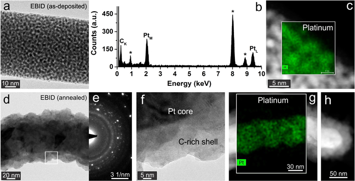
Figure 5. Structural and chemical analysis of an EBID Pt nanorod. (a) TEM micrograph of an as-deposited nanorod section. (b) EDX spectrum of the nanorod in (a); the * signal peaks from the Cu grid. (c) STEM image of the nanorod in (a) with an overlaid EDX map of Pt. (d) TEM micrograph of an annealed nanorod. (e) Electron diffraction pattern of (d). (f) Detail of the annealed nanorod, as boxed in (d). (g) STEM image of the rod in (d) with an overlaid EDX map of Pt. (h) Tip of an annealed nanorod.
Download figure:
Standard image High-resolution image2.4. Discussion
The above results shed light on how electrodes fabricated with IBID and EBID respond to thermal annealing and explain why this processing step can be so effective in minimizing contact resistance for EBID devices.
In our IBID devices, with the exception of the outer layer of carbon, the annealed electrodes did not change much, electrically or structurally (figure 6(a)). Despite knowing that Ga and Pt are not the most active catalysts for the growth of nanostructured carbon, their presence may have facilitated its diffusion. Subsequent deposition in the electrode's surface resulted in a wider carbon coating. The intrinsic presence of this shell likely stabilized the entire structure as it restricted major structural rearrangements with heating. These observations point to an arrangement of the electrode–interconnect interface that is different from the classically assumed metal–nanostructure. Instead, it is more plausible to envisage a Pt–(carbon shell)–CNT configuration. The increased thickness and structural ordering of the carbon shell upon annealing would lead to the optimization of the contact interface. Whether charge transport is driven along the carbon layers and/or in the Pt core is presently an open question.

Figure 6. Schematics of thermally-induced structural changes in beam-deposited Pt electrodes (not to scale). (a) IBID electrode on a SiO2/Si substrate, before and after annealing, where the gray color stands for C and the light brown for Pt; the height h of the electrode remains approximately the same. (b) EBID electrode on a SiO2/Si substrate, before and after annealing; a height difference (Δh), increased surface roughness and formation of a core–shell are observed.
Download figure:
Standard image High-resolution image
In the case of the EBID devices (figure 6(b)), as the annealing took place, the Pt particles sintered and the amorphous carbon diffused outwardly forming carbon platelets with similar lattice structure to those of the IBID shells (as per the Raman analysis). Here, the structural rearrangements explain why the electrical response differed so much from the as-deposited to the annealed systems. Initially, the CNT is contacted to a dielectric carbon matrix and dispersed Pt particles, implying that charge conduction paths are mostly broken or non-existent. Post-annealing, these paths are assembled in the form of the outer carbon shell which further defines the contact interface as Pt–(carbon shell)–CNT, just as for the IBID case. Finally, it is interesting to note that the overall conductance in the annealed EBID devices is higher than in the IBID ones and that the contact resistance is also smaller in the first.
3. Conclusion
IBID and EBID electrical devices containing CNT interconnects were fabricated and characterized pre- and post-annealing. Pt nanorods were used as model structures to study the response of the Pt leads to heat. While IBID devices are affected little by the thermal process, the EBID ones change significantly, both electrically and structurally. The identification of an ordered carbon shell on the Pt leads defines a dual interface contact and helps explaining the optimized charge transport observed for the devices. The post-annealing electrode–interconnect interfaces are more efficient in EBID and therefore better serve the purpose of fabricating electrical devices for carbon nanostructures when using direct deposition methods.
4. Experimental section
4.1. Preparation of patterned SiO2 /Si substrates
Commercially available 4'' SiO2/Si wafers were used to place the first 1 cm × 1 cm pattern, prepared using laser beam lithography (Heidelberg DWL2000). The pattern was composed of multiple 50 μm × 50 μm squares, each separated by 20 μm, and arranged in nine rows and columns. After exposure and development, 85 nm of Pt was deposited using sputtering (AJA international Inc. ATC2000). The lift-off step was carried out with ultrasonication, in acetone. Finally, the patterned 4'' wafer was cut into 1 cm × 1 cm pieces.
4.2. Dispersion of MWCNTs
A 4'' SiO2/Si wafer covered with a mat of plasma-enhanced chemical vapor deposition (PE-CVD) grown MWCNT was received from AIXTRON Ltd, UK. A small piece of the wafer was cut and ultrasonicated (Branson MT-5510) in ethanol to prepare the nanotube's suspension. This was then drop-cast onto the patterned substrate in order to obtain individual MWCNT. To eliminate the excess solvent or possible water residues, the patterned substrates bearing the dispersed nanotubes were dried on a hotplate at 100 °C for 30 min.
4.3. Contact fabrication
To fabricate metal contacts and integrate the MWCNTs into electrical devices, a dual-beam electron microscope (FEI Helios Nanolab 400S) was used in either IBID or EBID mode. Following preliminary tests, the following deposition parameters (accelerating voltage with constant beam current) were used to prepare devices with EBID and IBID, respectively: 1.4 nA at 5 kV and 43 pA at 30 kV.
4.4. Characterization
The electrical measurement was carried out on a conventional probe station (Cascade M150) in four-probe configuration and recording current versus voltage curves (Keithley 2410C or Keithley 4200). In order to avoid unintentional structural changes in the electrodes, the lower range of current was used for short periods of time. Errors in the resistance values were minimized to less than 2% by controlling the measurement parameters and conditions employed. Raman spectra and maps were collected with a 532 nm laser source at 100× magnification and with a laser power below 1 mW (WITec Alpha300RA). Deconvolution of Raman peaks was performed with Gaussian fits. For device mapping, an area of 15 μm × 15 μm was scanned and the D and G band signals were extracted using a window of 150 cm−1. SEM images were taken on an FEI Nova Nano. For TEM analysis, MWCNTs were suspended in ethanol and drop-cast onto a 300 mesh Holey carbon grid. The EBID Pt and IBID Pt deposition of free-standing nanorods were carried out at 43 pA (5 kV) and 1.5–93 pA (30 kV), respectively, on a bare Cu TEM grid and using an FEI Helios Dual Beam system. High-resolution images were taken on a FEI TITAN, operating at 300 kV. Electron diffraction patterns were obtained for the nanorods at the same location where the EDX were taken. The chemical composition of IBID Pt nanorods was mapped, before and after the heat treatment, with EELS. The chemical composition of EBID Pt nanorods was mapped, before and after the heat treatment, with EDX using a 200 kV FEI Titan ChemiSTEM. For the AFM analysis, a Park XE-100 was used to measure the diameter and length of MWCNTs in non-contact mode. The height and surface roughness of the IBID and EBID deposited electrodes were also measured, before and after the heat treatment, in contact mode.
Acknowledgments
AIXTRON Ltd, UK, is acknowledged for providing the MWCNT sample. NMB and AA thank KAUST for graduate scholarships. We are grateful for research funds from KAUST (BAS/1/1346-01-01/02).