

Abstract
Two-dimensional materials and their heterostructures have emerged as a new class of materials, not only for fundamental physics but also for electronic and optoelectronic applications. Black phosphorus (BP) is a relatively new addition to this class of materials. Its strong in-plane anisotropy makes BP a unique material for making conceptually new types of electronic devices. However, the global density of states (DOS) of BP in device geometry has not been measured experimentally. Here, we report the quantum capacitance measurements together with the conductance measurements on an hBN-protected few-layer BP (∼six layers) in a dual-gated field effect transistor (FET) geometry. The measured DOS from our quantum capacitance is compared with density functional theory (DFT). Our results reveal that the transport gap for quantum capacitance is smaller than that in conductance measurements due to the presence of localized states near the band edge. The presence of localized states is confirmed by the variable range hopping seen in our temperature dependence conductivity. A large asymmetry is observed between the electron and hole side. This asymmetric nature is attributed to the anisotropic band dispersion of BP. Our measurements establish the uniqueness of quantum capacitance in probing the localized states near the band edge, hitherto not seen in conductance measurements.
1. Introduction
Black phosphorus (BP) is a recent addition to the family of 2D materials like graphene, hBN and layered transition metal dichalcogenides (TMDs) [1, 2]. BP has a layer-dependent direct band gap at Γ-point (∼1.7 eV for the monolayer and ∼ 0.3 eV for the bulk), [3–8] lying between the two extremes of other 2D materials, namely semimetallic graphene (no gap) and insulating hBN. The unique aspect of BP is the puckered honeycomb structure of the layer, having two kinds of P–P bonds: the shorter bond length (2.224 Å) connecting the nearest P atoms in the same plane and the longer bond length (2.244 Å) connecting P atoms between the bottom and top of a single layer. Furthermore, the edges are zigzag and armchair along two orthogonal directions, resulting in anisotropic electronic transport [4, 9–11] and optical absorption [3–5]. The effective mass of electrons along the zigzag is ∼ 10 times higher compared with that along the armchair direction. [1] This in-plane anisotropy makes it a unique and attractive choice for electronic and optoelectronic applications covering mid-infrared to visible range. [12]. Field effect transistors have been reported for few-layer BP, [2, 10, 13, 14] showing on/off ratio of as well as high mobility (∼1000 cm2 V−1 s−1), thereby combining the good aspects of graphene (high mobility) and MoS2 (high on/off ratio).

In a classical capacitor, capacitance is only determined by the geometry (CG), where the electrons distribute themselves in such a way that the electrostatic energy inversely proportional to capacitance is minimized. However, the addition of an electron requires extra kinetic energy and therefore contributes to the total capacitance 1/C = 1/C + 1/C where CQ is the quantum capacitance [15]. The quantum capacitance directly probes the electronic density of states (DOS) of the material [16, 17]. As a result, quantum capacitance can give better insight into the localized states near the band edge of a semiconductor compared to the conductance measurement. Quantum capacitance measurements have been shown to provide significant insights into the ground state of low dimensional systems such as electron–electron interactions, quantum correlations, [16] thermodynamic compressibility for 2D electron gas in GaAs heterostructures [18] and many-body physics in carbon nanotubes, [16] and graphene [19–23]. Capacitance spectroscopy has also been used to probe metal-insulator transition in MoS2 [24].


To investigate the DOS of BP near the band edge, we report here for the first time the quantum capacitance measurements together with the conductance measurements of few-layer BP (∼six layers) at the low temperatures of 77 K and 4.2 K as a function of the back and top gate voltages. For the later geometry, an ultrathin hBN layer (∼25 nm thick) has been used as a dielectric which also helps to protect the BP from atmospheric degradation. We compare our quantum capacitance results with the derived density of states based on the density functional theory (DFT). We show that the transport gap from the capacitance measurements is much smaller as compared to that deduced from the conductance measurements. Our results reveal a large asymmetry (∼15 times) in the onset voltages between quantum capacitance and conductance for both the electron and hole sides. These results have been explained in terms of localized states near the band edge as well as asymmetric band dispersion (seen in the DFT) along the zigzag direction (Γ-Y) for the electron and hole carriers. The presence of localized states is confirmed by the variable range hopping seen in our temperature dependence conductivity at different values of hole doping achieved by back gate voltage. We have also carried out similar measurements on a few layer MoS2 device and observed a much smaller onset difference between the capacitance and the conductance data.
2. Results and discussion
In order to measure the quantum capacitance of few-layer BP we have used dual-gated field effect transistor geometry as shown schematically in figure 1(a). Figure 1(b) shows the optical image of the device, where few-layer BP mechanically exfoliated from the bulk single crystal (M/s Smart Elements) has been transferred onto a degenerately-doped silicon wafer with 285 nm SiO2 on top. The samples were immediately coated with a PMMA layer to prevent degradation of the BP. After optical inspection we chose a very thin BP flake for the device. The electrical contacts were fabricated using electron beam lithography with Cr/Au (5nm/70nm) contacts deposited using thermal evaporation at a base pressure of ∼3 × mbar. Using the dry transfer technique described in [25], a thin layer of hBN was transferred immediately after lift-off onto the exposed region of the BP flake, which served as a passivation mask as well as a top gate insulator (inset of figure 1(b)). The sample was characterized by an atomic force microscope and Raman spectroscopy (figure 1(c)). The AFM height measured on our sample was ∼3 nm corresponding to ∼six layers. All the transport measurements were carried out at 4.2 K and 77 K at a base pressure of ∼1 × mbar inside a home-built dip-stick cryostat. The hBN-protected few-layer BP was stable for more than a month without any degradation at low temperatures.


Figure 1. (a) Schematic of the dual-gated few-layer BP device. (b) Optical image of the device. Scale bar = 10 μm. The black dotted line shows the region of the top gate which is shown in the inset. (c) AFM image of the BP (left) with scale bar 100 nm. Inset shows the height profile corresponding to 3 nm BP height (shown by horizontal dashed lines). DFT optimized structure of the six-layer BP (middle). Raman spectra of the BP sample (right). (d) Schematic of the capacitance measurement using a differential current amplifier (CA). CQ + CG represents the total capacitance between the TG and BP whereas represents parasitic capacitance between the top gate bonding pad and source drain bonding pad. represents the parasitic capacitance between the top gate bonding pad and a dummy bonding pad (not connected with the device having an exact dimension of source and drain bonding pads). LA stands for lock-in amplifier.


Download figure:
Standard image High-resolution imageThe two probe conductance measurements between the source and drain were carried out using a low frequency (∼1 kHz) lock-in technique with a small excitation voltage of 10 mV (at 77 K) and 1 mV (4.2K), using a home-built current amplifier [26] with a gain of 107. For the capacitance measurements we used the circuit diagram as shown in figure 1(d), [17] using a home-built differential current amplifier. The capacitance has been measured between the top gate and black phosphorus with a small excitation voltage of 10 mV at ∼1 kHz frequency with a resolution of ∼2 fF. The parasitic capacitance (CP) was ∼100 fF, which reduced to ∼10 fF after using differential schemes as mentioned above. This value of CP was subtracted from the measured capacitance data presented in this paper.
As shown in figure 1(a) the capacitor is formed between the top gate and the central part of the BP beneath the gate. Figures 2(a) and (b) show the conductance map measured at 77 K and 4.2 K, respectively, as a function of the top gate (VTG) and back gate voltages (VBG). The VTG controls the carrier concentration (Fermi energy) in the central part of the BP whereas the back gate controls the carrier concentration throughout the sample, giving n-p-n- or p-n-p-like geometries. In principle, an intrinsic semiconductor will conduct whenever the Fermi energy touches the conduction or the valence band edge. In our device, high conductivity is observed only when both sides near the leads and the central part have hole doping (negative gate voltages), showing that BP is unintentionally p-doped at zero gate voltages, as known from earlier studies [2]. From a −5 V to a 0 V top gate voltage, the onset of conductivity starts at a constant back gate voltage as the Fermi energy touches the valence band edge of the leads. However, from a 0 V to a +2 V of VTG the onset of conductivity depends on both the top and back gate voltages. Along the dashed diagonal lines in the two-dimensional plot of figures 2(a) and (b), the Fermi energy touches the valence band edge of the central part of the device. From this slope ∼ 11 we estimate the thickness of the top hBN to be ∼25 nm ( × dTG = × dBG, dBG = 285 nm, where we have taken the dielectric constant ∼ = 3.9). In figure 2(c) we have shown conductance in a logarithmic scale as a function of VBG at VTG = 0 V (along the vertical dotted line in figures 2(a) and (b)) for 77 K and 4.2 K. The on/off ratio in our top-gated device is ∼105 as can be seen from figure 2(c) and the field effect mobility measured at 77 K was ∼20 cm2 V−1 s−1 at VBG ∼ −28 V, as estimated using the relation ( and CG = 1.2 ×10⁻⁸ F cm−2). At 77 K we observe the onset of conductance for valence (conduction) bands at −3 V (+50 V), whereas at 4.2 K we only see it for the hole side at −33 V. The main striking differences at the two temperatures are the following: with increasing negative back gate voltages the conductance increases smoothly at 77 K, whereas at 4.2 K it increases with superimposed random fluctuations. Secondly the onset of conductance with the back gate voltage for the hole side increases from 77 K to 4.2 K. These shifts in the onset of conductance with a lowering of the temperature can be explained by the mobility edge picture having localized states [27]. The mobility edge can shift in energy, as the thermally activated transport becomes weaker with the lowering temperature, as explained by Mott's variable range hopping (M-VRH) model [28, 29]. To verify localization near the band edge we have measured the temperature-dependent conductance for the hole side as shown in figure 2(d) (see supplementary information for the details). The data fits very well with the M-VRH with


where σ is the conductivity, d is the dimensionality of the system, T0 is the correlation energy scale and = ATm with m 0.8. The values of T0 are shown in the inset of figure 2(d). From the values of T0 (for VBG = −20 V) and using = , and taking the surface density of electron–hole puddles at the SiO2 interface [30] = 4 ×10¹² eV−1 cm−2, the localization length ξ is 11 nm similar to other 2D materials like MoS2 [30] and WSe2 [31]. These localized states are mostly created due to the charge in homogeneity in the underlying SiO2 layer as well as the defects in BP. Please note that consideration of contact resistance in our analysis may change the values of T0. However, it will not alter the main inference drawn as the existence of localized states near the band edge.


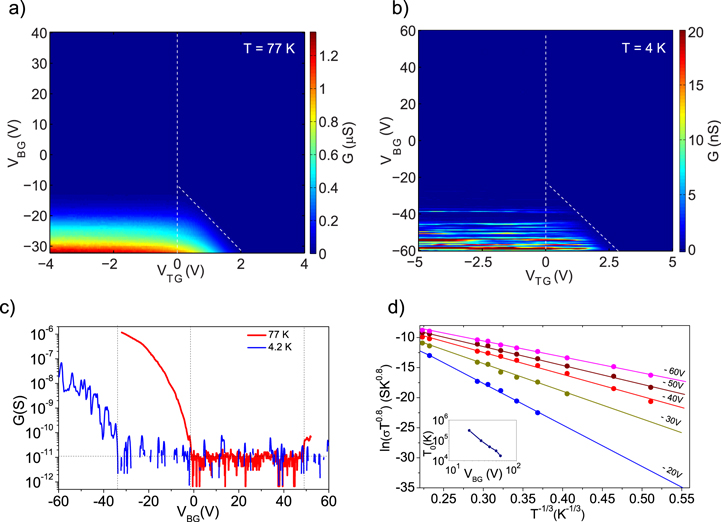
Figure 2. Conductance as a function of VBG and VTG at 77 K (a) and 4.2 K. (b) Vertical white dashed lines show VTG = 0 V cut line. (c) Conductance as a function of VBG at VTG = 0 V at 77 K and 4.2 K. Vertical black dashed lines show the onset of conductance. (d) Temperature-dependent conductivity and variable range hopping at different back gate voltages. The solid lines are the fit to equation (1). Inset shows T0 for different VBG.
Download figure:
Standard image High-resolution imageWe will now present the quantum capacitance measurements. Figures 3(a) and (b) show the measured total capacitance as a function of VTG and VBG at 77 K (4.2 K). The four corners of the plots are marked with p-p-p, p-n-p, n-p-n, n-n-n, specifying the carrier types near the left side lead, the central part and near the right side lead of the BP. The total capacitance of the central part is zero in the blue region of the 2D plots and it becomes finite, of the order of ∼70 fF, as shown by the red region in the 2D plots for both the p-p-p and n-n-n regions. This is in contrast with only the hole side conductance (figures 2(a) and (b)). The diagonal dashed lines in figures 3(a) and (b) indicate the onset of Fermi energy to the band edge in the central part of the BP, whereas the horizontal dashed lines show the onset of Fermi energy to the band edge of the leads for both types of carriers. Even though we are measuring the capacitance of the central part of the BP, we need to tune the leads for p or n types such that the charging time (RCT) of the central part through the lead resistance (R) becomes smaller than the time period (∼1 ms) of our ac excitation frequency (∼1 kHz). For measuring a capacitance of 1 fF in the central part, the maximum lead resistance (R) has to be less than 1000 GΩ. The diagonal dashed lines in figures 3(a) and (b) give the hBN thickness to be ∼25 nm, in agreement with the conductance measurements. Figure 3(c) shows the total capacitance as a function of VBG at VTG = 0 V at 77 K and 4.2 K. As mentioned before, 1/CT = 1/CG + 1/CQ, therefore, if When the Fermi energy is inside the band gap, will be zero (DOS is zero) and hence CT will be zero. On the other hand, when the Fermi energy is within the conduction or valence band, CQ will be much higher than CG and therefore, At both temperatures in figure 3(c), the measured CQ is zero for a certain range of back gate voltages and increases sharply on both sides, saturating to ∼ 70 fF. The measured fF matches very well with the estimated CG = for the gate area (A) of ∼50 μm2 (determined from the optical image of the top gate as shown in figure 1(b) with d = 25 nm thick hBN). It can be seen from figure 3(c) that the onset of CQ at 77 K is 0 V (hole side) and + 20 V (electron side) whereas at 4.2 K the onset voltages are −10 V and + 30 V. The shift in the onset of gate voltages with lowering temperature is symmetric for both types of carriers, but there are only fluctuations in CQ (4.2 K) near the onset on the electron side (figures 3(b) and (c)), probably indicating that the localized states near the electron side are greater compared to those near the hole side. The extracted CQ as a function of VBG is shown in the inset of figure 3(d).


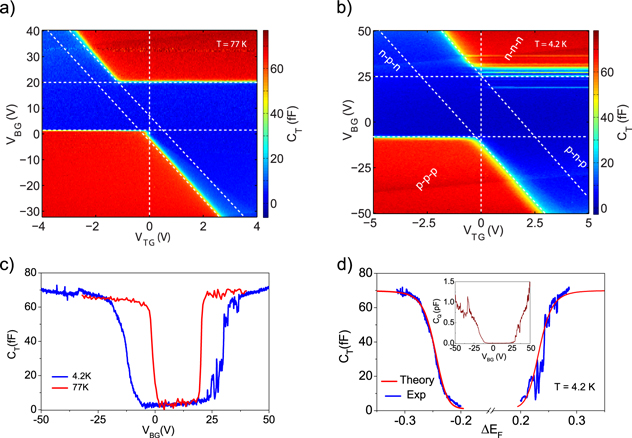
Figure 3. Total capacitance as a function of VBG and VTG at 77 K (a) and 4.2 K (b). (c) Total capacitance as a function of VBG at VTG = 0 V at 77 K (red) and 4.2 K (blue) along the vertical dashed lines in figures (a) and (b). (d) Comparison between the experimentally measured total capacitance at 4.2 K (blue curve) versus the theoretical one (DFT) as a function of Fermi energy (red curve). Inset shows the quantum capacitance as a function of the back gate voltage.
Download figure:
Standard image High-resolution imageIn order to compare the CQ with the calculated DOS we need to convert the gate voltages into Fermi energy. EF = αVG ( is a conversion factor) when the Fermi energy is inside the band gap and EF = for the case of Fermi energy in the band. In order to get α, we have taken the band gap of BP (∼six layers) to be ∼400 meV [2, 8, 10] and α becomes 0.013 (ΔVG/ΔEF = 30/0.4 using the 4.2 K data). Now, to determine in the band, we have used the following method. The induced carrier concentration (n) in the sample can be determined by


at different VG using 4.2 K data from figure 3(c). From the DFT calculation we have calculated the carrier concentration (n) as a function of Fermi energy for six-layer BP. By mapping experimentally determined with theoretical VG is converted into Fermi energy (see supplementary information for details). We performed first-principles DFT calculations using the pseudopotential plane wave method as implemented in the Quantum ESPRESSO [32] package. A vacuum of 15 Å was employed to avoid spurious interactions between the six-layer phosphorene and it's periodic images in the out-of-plane direction. We used norm-conserving pseudopotentials [33] and accounted for the van der Waals interaction between the layers using the Grimme-D2 [34] formulation. The wavefunctions were expanded in plane waves with energy up to 60 Ry, and the Brillouin zone sampled with a 14 × 10 × 1 k-point grid. The calculations were performed using the Heyd Scuseria Ernzerhof (HSE) [35] as well as the Perdew–Burke–Ernzerhof (PBE) [36] exchange correlation functionals. Within PBE, our calculated structural parameters are in excellent agreement with the previous results [37]. However, the calculation within PBE results in a semi-metallic system. This is in contradiction with the experimental result that six-layer phosphorene is a semiconductor. The band gap of phosphorene is known to reduce with an increasing number of layers [37]. This, coupled with the well-known underestimation of the band gap within Kohn-Sham DFT results in a closing of the gap [3]. This trend has been reported in the literature and our calculations are in agreement with the previously reported results [37]. While the band gap closing is unphysical, other features of the band structure are unaltered and follow the trends with layer size. To fix the above-mentioned problem with the band gap, we performed calculations with the HSE exchange correlation functional. The atom positions here are taken from the PBE relaxed structure. The k-point sampling for the non-local Fock exchange operator is chosen to be 7 × 5 × 1 for ease of computation. In order to calculate the density of states on a fine grid of k-points, we transformed the HSE wavefunctions to maximally localized Wannier functions using the Wannier90 [38] package. The DOS was then obtained from a 448 × 320 × 1 k-point grid. The full DOS of six-layer BP has been shown in figure SF2 in the supplementary information. The HSE calculation results in a rigid shift of the PBE valence and conduction bands leading to the opening of a band gap. We find the HSE band gap to be about 1 eV, which is larger than the previously reported values. We attribute this discrepancy to the presence of a strain in our structure and the Brillouin zone sampling for the Fock exchange. To compare the theoretical DOS with the experiment we added a Gaussian broadening of 50 meV and rigidly shifted the gap to 400 meV, as reported earlier [2, 8, 10]. The theoretical CQ has been calculated using the relation and in figure 3(d) the solid red line shows the theoretical CT (with CG = 70 fF), which matches very well with the experimental CT (solid blue line).


Now we will move to the main striking result of this paper. In figure 4 we have compared the onset of conductance versus the onset of quantum capacitance at 77 K (figure 4(a)) and 4.2 K (figure 4(b)). At 77 K, the differences between the onset voltages ΔV = − are ∼2 V for the hole side and for the electron side. At 4.2 K, is ∼20 V, whereas we could not measure because even up to a VBG of 70 V, the device was in the off-state in the conductance measurement. Quantum capacitance directly measures the DOS, and therefore it can probe the localized states near the band edge as long as charging takes place. On the other hand, conductance through the channel will occur when the Fermi energy crosses the mobility edge into the extended states, thereby justifying a finite value of ΔVonset. However, the large asymmetry between the ΔV and ΔV () is still to be explained. Can this large value of R arise from the different values of mobilities of electrons and holes ( 20 cm2 V−1 s−1 and 10 cm2 V−1 s−1)? To address this point, we took similar measurements on few-layer MoS2 at 77 K having 10 cm2 V−1 s−1 (comparable to that of (BP)). Figure 4(c) shows that for 3 V—which is much smaller than the 30 V for the BP. We therefore infer that the large value of R may not be due to different values of mobilities of electrons and holes. The large value of R suggests that there are more localized states near the conduction band as compared to the valence band, shown schematically in figure 4(d). It is likely that an asymmetry in electronic structure between the electron and hole sides along the (Γ-Y) direction (highlighted in figure 4(e)) can contribute to the above observations. Indeed, Yuan et al show that the mid-gap states, preferentially near the conduction band, are created due to point defects in bilayer BP (see figure 3(b) in [11]). However, a quantitative understanding is yet to emerge for our system.


Figure 4. Onset of conductance (blue) and capacitance (red) as a function of VBG at 77 K (a) and 4.2 K (b) and (c) for few-layer MoS2. (d) Schematic of the DOS as a function of energy. (e) Calculated band structure of six-layer BP. The asymmetry between the electron and holes along the Γ-Y direction is highlighted by a blue dotted circle.
Download figure:
Standard image High-resolution image
3. Conclusion
In summary, we have measured the quantum capacitance along with the conductance of hBN-protected six-layer BP at low temperatures using both back gate and top gate voltages. The measured capacitance as a function of doping matches the DFT calculations. The differences in the onset between the conductance and quantum capacitance measurements for the electron and hole sides attributed to the presence of localized states and anisotropic band dispersion still need a better theoretical understanding. Our results show that quantum capacitance can probe the localized states of a two-dimensional semiconductor which cannot be measured by conductance measurements. It would be worth measuring the quantum capacitance of BP as a function of the number of layers.
Acknowledgments
M Jain thanks the Supercomputing Education and Research Center, IISc for the computational resources. A K Sood thanks the Department of Science and Technology, India under the Nanomission project for financial support. A Das thanks the Department of Atomic Energy and the Indian Institute of Science start-up grant for financial support.