
Abstract
Using out-of-plane magnetized layers, a lateral shift register made from discrete elements is demonstrated. By carefully designing the in-plane shape of the elements which make up the shift register, both the position of nucleation of new domains and the coercivity of the element can be controlled. The dipole field from a neighboring element, placed tens of nanometers away, creates a bias field on the nucleation site, which can be used to create a NOT gate. By chaining these NOT gates together, a shift register can be created where data bits consisting of neighboring layers with aligned magnetization are propagated synchronously under a symmetric applied magnetic field. The operation of a 16 element shift register is shown, including field coupled data injection.
Export citation and abstract BibTeX RIS

Original content from this work may be used under the terms of the Creative Commons Attribution 3.0 licence. Any further distribution of this work must maintain attribution to the author(s) and the title of the work, journal citation and DOI.
Introduction
The highly nonlinear switching and non-volatility of magnetic materials makes them ideal candidates for implementing logic operations [1]. In particular, perpendicularly magnetized materials have the advantages of narrow, fast-moving domain walls [2] and high bit stability at small lateral sizes [3] due to the relatively large anisotropies that can be achieved in such systems. Using these materials, data bit storage and various types of logic devices have been demonstrated [4–9]. One commonly used sequential logic device is the shift register, whose state is a function of both current inputs and its history, which is used in data storage, timing and converting between serial and parallel interfaces. Data is propagated along a chain [4, 8, 10–12], which can, for instance, be made from a series of NOT gates. This is easily designed in perpendicularly magnetized materials due to the antiferromagnetic dipole coupling between laterally spaced elements [13–15]. However, a careful design of each element making up the chain is required to achieve an asymmetry in the effect of the dipole field [15], in order to create a well-defined propagation direction [5]. Previously, unidirectional propagation of data in perpendicularly magnetized materials has been achieved by selectively lowering the nucleation field at a specific site using focussed ion beam irradiation [5, 7, 14]. In this paper we show a different approach in which the size-dependent coercivity of a nanowire is used to break the symmetry and hence create unidirectional propagation. We demonstrate a lateral shift register made from up to 16 elements. The design of each element allows unidirectional propagation and also creates a field coupled input to the shift register allowing the injection and synchronous propagation of data bits along the chain. This work is a step towards the implementation of logic functions in magnetic materials that could lead to non-volatile, low energy electronic devices.
Methods
Nanowires and shift register elements are created using e-beam lithography with PMMA resist, magnetron sputtering and liftoff on Si substrates. The magnetic films are based on repeated CoFeB/Pt layers with a Ta/Pt buffer in order to give a large perpendicular anisotropy, whilst increasing the moment of the wire compared to single magnetic layers. The wires and elements are measured by focussed laser polar magneto optical Kerr effect (MOKE) and polar Kerr microscopy.
Results
Rectangular nanowires
The underlying device physics which allows a shift register to be created is shown in figure 1. In figure 1(a) the switching fields of rectangular nanowires of different widths made from a Ta (4 nm)/Pt (6 nm)/[CoFeB (0.7 nm)/Pt (0.6 nm)]4/Pt (3 nm) stack are shown. As the wires become narrower there is a reduction in the coercivity, and it has been shown that for the narrower wires nucleation of new domains occurs from the ends of the wire [15, 16]. Another feature of these wires is shown in figure 1(b), where the standard deviation of the switching field taken over an average of around ten wires is given, divided by the mean of the switching field. This shows a reduction of around a factor of two in the variability of the wire switching field for the narrower wires compared to the wider ones. This reduction in variability is important for making long chains of objects [14]. This reduction in variation is probably due to the nucleation occurring deterministically at the end of the nanowire, rather than at a defect somewhere within the wire.

Figure 1. (a) Switching field as a function of wire width for Ta (4 nm)/Pt (6 nm)/[CoFeB (0.7 nm)/Pt (0.6 nm)]4/Pt (3 nm) nanowires. (b) The standard deviation of the switching field for around ten wires divided by the mean switching field as a function of wire width.
Download figure:
Standard image High-resolution imageNOT gate
If a narrow wire is joined to a wider one the narrower wire can act as a domain wall injector for the element with a controlled nucleation position at the free end of the nanowire [15]. Such elements are shown in figure 2(a). Here, a 120 nm wide wire is smoothly attached to a 2 μm square. A domain wall will nucleate at the end of the wire and propagate through the rest of the element. Because the domain wall nucleation occurs at the same site in a rectangular nanowire and with the additional 2 μm square the switching field is the same for both [15]. In figure 2(b) a close up of two elements is shown. The free end of the wire is separated by a gap of around 40 nm from the neighboring element. The stray field from one element will act upon the other. Because the free end of the wire nucleates at lower fields than the body of the 2 μm square the wire will switch first upon reversing an applied magnetic field. This breaks the symmetry with respect to the two neighboring elements and creates a defined direction for the propagation of information. The slight recess in the 2 μm square is designed to increase the effective stray field on the end of the nanowire [13, 14] (see also supplementary material is available online at stacks.iop.org/NANO/28/385201/mmedia).

Figure 2. (a) SEM image of a chain of elements forming part of the shift register. (b) Close up showing the narrow spacing between the wire and square element.
Download figure:
Standard image High-resolution imageTo illustrate this point more clearly we take a simple two element device shown in the insets to figure 3. A 2 μm square shape is placed next to the injector of a single element. When taking a hysteresis loop around only the lower coercivity element, we find that the hysteresis loop is shifted by around 100 Oe. This is due to the dipolar field of the 2 μm square acting on the end of the nanowire of the second element. This bias in hysteresis allows the creation of a NOT gate. A symmetric oscillating field can be applied, in this case with a magnitude of around 350 Oe, which switches neighboring elements from parallel to antiparallel but not the other way around, so that the second element will always switch to being antiparallel relative to the first element after a magnetic field cycle.
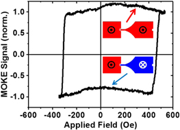
Figure 3. The minor MOKE loop taken around the right-hand element shown in the inset schematic. Note the shift in the loop with respect to field caused by the dipole coupling.
Download figure:
Standard image High-resolution imageShift register
We now demonstrate the shift register action of a chain of elements consisting of an initial square element, as in figure 3, followed by seven shaped elements. Figure 4(a) shows a set of Kerr microscopy images of this chain made of a Ta (4 nm)/Pt (6 nm)/[CoFeB (0.5 nm)/Pt (0.6 nm)]3/CoFeB (0.5 nm)/Pt (3 nm) magnetic layer stack. Due to the uneven lighting and the processing of the images in order to enhance the contrast, the elements appear widely separated whilst in reality they are as shown in figure 2. The top row shows the chain at positive saturation with each following row corresponding to the alternating application of  and
and  as indicated by the position of the green dots in figure 4(b). Here the applied field after saturation is ±500 Oe and Kerr images are taken at each field step. The integrated intensity for each element in figure 4(a) is shown in figure 4(c), and color coded according to the change in signal relative to the saturated state. The different intensities seen at saturation are due to the uneven illumination of the device. After the initial positive saturation, the −500 Oe field is enough to switch neighboring pairs from parallel to antiparallel but not the other way around. However, initially all neighboring elements are parallel to each other, so which layers switch on this initial step depends on the exact details of the nucleation of reversed domains in each element. As well as depending on small variations in lithography this is also a thermally activated process [17, 18]. In this example five elements switch leaving two pairs with parallel magnetization, as indicated by the rings (second row). As shown, it is possible for neighboring pairs to switch due to the time taken for a domain wall nucleated at one end of an element to reach the other end. On the application of a +500 Oe field the right hand side element of each pair switches up (third row). The effect of the switch, highlighted by the circles is clear. On each reversal of the field the switch of a single layer moves the position of the pair of parallel layers one to the right. The sign of the pairs also switches with each step. This pair of parallel layers, which can be considered as a soliton in a discrete antiferromagnetic lattice [11, 19], forms the data bit in the device and moves unidirectionally under an oscillating field [11, 14]. When the pair of layers reaches the end, it is expelled from the shift register and the chain reaches its ground state with all neighboring elements antiparallel. The raw and processed image data for this sequence are shown in a supplementary video.
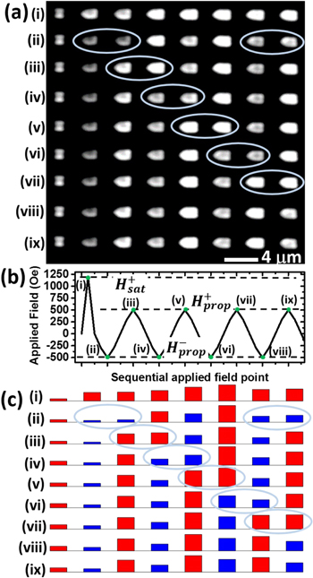
Figure 4. (a) A series of processed Kerr microscopy images of an 8 element shift register. Each row is taken at different applied field. The first row is positive saturation followed by images taken at alternating propagation fields. (b) The applied magnetic field sequence used to take the images in (a), the green dots indicate the field at which each row in figure (a) was taken. (c) The integrated intensity of the elements shown in (a). The color code indicates whether the magnetization is up (red) or down (blue). The rings indicate the position of the data bit.
Download figure:
Standard image High-resolution imageThis idea can be extended by allowing new data bits to be injected at the start of the chain. This is shown in figure 5 for a 16 element chain. The first row shows the negative saturation state, after which the data shown is taken from the middle of a sequence where an oscillating applied field is used to propagate data bits similarly to figure 4. However, now the first element, rather than being a square, is the same as the other elements. Because there is no dipole field acting on the free end of the wire the nucleation field of this element is higher. This allows a slightly larger field to be applied,  , which leads to switching of the first element as well as propagating data along the chain. The applied field is shown in figure 5(b) along with the integrated signal from each element in figure 5(c). Again the data is color coded according to the change in intensity relative to the saturation level. New data bits are created by applying
  of alternating sign, an example with negative injection field is shown on figure 5. This can also be seen in a supplementary video.
  naturally lies between the propagation and saturation fields due to the design of the device. The ability to propagate over longer chains is limited by the variation in the lithography which changes the nucleation field and the dipole coupling strength.

Figure 5. (a) A series of processed Kerr microscopy images of an 16 element shift register with injector. Each row is taken at different applied field. The first row is negative saturation followed by a set of images taken at alternating propagation fields or the injection field. (b) The applied magnetic field sequence used to take the images in (a), the green dots indicate the field at which each row in figure (a) was taken. (c) The integrated intensity of the elements shown in (a). The color code indicates whether the magnetization is up (red) or down (blue). The rings indicate the position of the data bits.
Download figure:
Standard image High-resolution image
Discussion
The experiments presented here show how data can be injected and propagated synchronously along chains of elements. The correct operation of the ratchet occurs only after a certain number of propagation cycles of the field have been performed after saturation, which removes the data bits created stochastically. The device could be improved by reaching a deterministic state after saturation where all neighboring layers are antiparallel. This could be achieved by changing the nanowire width slightly on every other element leading to a well-determined order of switching during the first field cycle. The elements used are relatively large in order to aid the imaging via MOKE microscopy. However, as shown by figure 1(a), the underlying physical properties used to create the elements can be easily scaled down to hundreds of nanometers, a length scale widely used in nanomagnetic logic devices [4, 10, 20]. A reduction in the width would also lead to a reduction of the required field for propagation. Also, the timescale of the experiment shown here is slow, with each field step being held for a few seconds. The limiting timescale in perpendicular devices depends on the times of both domain wall propagation and nucleation. The propagation speed depends on the size of the applied field as well as the number and magnitude of pinning sites in the material. However, domain wall velocities can typically reach hundreds of meters per second in the flow regime [21]. For elements a few hundred nanometers across propagation times would, therefore, be around tens of nanoseconds. The timescale for nucleation is also dependent on the field. In perpendicular materials nucleation is a strongly thermally activated process and so can vary dramatically for small changes in sample or applied field conditions. It has been shown that for dipole coupled perpendicular magnets that switching times of the order of tens of nanoseconds are to be expected [22]. Therefore an optimized system may be able to operate in the 10–100 MHz range. Recent developments in the switching of elements and domain wall propagation by in-plane current [23–25] may also enable current pulse, rather than field pulse, based clocking in similar structures and the initial feasibility of such an approach has already been demonstrated [25]. One promising direction is geometrically controlled switching through the spin orbit torques, where elements are deterministically switched by domains are nucleated at the ends of shaped elements [26], which could profitably be integrated with this work. Current driven devices could allow even faster clocking speeds than field pulses.
This work, combined with vertical magnetic logic structures [9, 11], could also allow data to be propagated both laterally and vertically allowing new logic architectures to be designed.
Conclusion
By exploiting the width-dependent coercivity of perpendicularly magnetized nanowires, the site of nucleation in elements with a designed in-plane shape can be controlled. By chaining such elements, with a small lateral gap, dipole coupling allows the creation of a simple logic device. The dipole coupling favors an antiferromagnetic alignment of neighboring layers and allows a data bit consisitng of two parallel aligned neighboring layers to be propagated along the chain. The first element in the chain naturally acts as an injector of new data bits and can be activated by use of slightly higher fields than those used to propagate the bits. A shift register inverter chain with 16 bits has been demonstrated and shows the effectiveness of perpendicularly magnetized materials for nanomagnetic logic operations.
Acknowledgments
This research is funded by the European Community under the Seventh Framework Program ERC Contract No. 247368: 3SPIN, and by EMRP JRP EXL04 SpinCal. The EMRP is jointly funded by the EMRP participating countries within EURAMET and the EU. AB acknowledges DTA funding from the EPSRC. AFP acknowledges support from the EPSRC Early Career Fellowship EP/M008517/1 and a Winton Fellowship. The underlying data for this study are available at https://doi.org/10.17863/CAM.10557.