

Abstract
The formation, including the density and height of the InFeP:Ag nanorods doped with noble metal Ag using an ion milling method, was preponderantly determined from transmission electron microscopy and x-ray diffraction analyses. We investigate, in particular, the enhanced ferromagnetism of the well-aligned InFeP:Ag nanorods. Auger electron spectroscopy and x-ray photoelectron spectroscopy measurements were carried out in order to investigate the incorporation of Ag and to verify the local chemical bonding of the InFeP:Ag nanorods. The variation of FWHM for the double-crystal x-ray rocking curve and triple-axis diffraction peaks demonstrates that noble metal Ag is incorporated into the InFeP:Ag nanorods. The noticeable ferromagnetic signature (M-H curve) of the InFeP:Ag nanorods is observed and Tc persists up to almost 350 K (3.9 × 10⁻⁴ emu g−1), as determined by temperature-dependence magnetization (M-T curve) measurements. This study suggests that the InFeP:Ag nanorods should be a potential candidate for the application of spintronic devices.
Export citation and abstract BibTeX RIS
1. Introduction
Recently, a great deal of effort has been devoted to achieving ferromagnetism above room temperature, including transition metal (TM) elements, because of the high demand for advanced spintronic devices in diluted magnetic semiconductors (DMSs) [1–4]. The InP based on DMS with TM elements has already been studied [5–7] and we continue to investigate various characteristics in order to enhance the Curie temperature without clusters. One-dimensional (1D) nanostructure semiconductors have received special attention due to their great prospects in unique structural one-dimensionality, possible quantum confinement effects, and novel nanoscale device applications. Therefore, 1D nanostructure semiconductors were used in various areas such as material sciences, electronics, optics, and magnetics [8–12]. The magnetic properties of materials can be generally caused by the size dependence as a result of various effects such as the influence of the surface, the quantum confinement, and the reduction of structure size below that of a single magnetic domain [13–19]. It is possible to enhance or even induce magnetic behavior by changing the dimensionality of a system. Magnetic nanorods are a comparatively recent focus of attention [15, 16]. In addition to exhibiting large anisotropy, 1D magnetic nanostructures can act as their own interconnects, making them attractive for use in sensing and as active elements in spintronic devices. The magnetic properties of InP based on 1D nanostructures doped with TM elements have been studied for the application of nanoscale spintronic devices [12, 20–22]. However, further investigations of 1D nanostructure InP-based DMSs reveal that we still require great ingenuity to realize their application in practical spintonic devices.
In considering the above requirements, InFeP:Ag nanorods were fabricated and various characteristics related to InFeP:Ag nanorods are dealt with in this paper. The formation of InFeP:Ag nanorods was performed using an ion milling method subsequent to novel metal silver (Ag) deposition, so as to develop the fabrication of 1D nanorods by another, facile method. Together with the formation of InFeP:Ag nanorods, the magnetic properties of the InFeP:Ag nanorods were further investigated for various applications such as optical detectors, light-emitting diodes, and spintronics. It is noted that noble metal was used, so as to grow the formation of nanorods and wires as a catalyst in the area of nanostructure. However, in our recent study, Ag itself was used as a dopant in order to make the InZnP:Ag nanorods [23]. In this study, our samples doped with noble metal Ag were used in order to investigate various physical properties, especially magnetism including the formation of nanorods. The physical properties of the samples were characterized by means of Auger electron spectroscopy (AES), x-ray photoelectron spectroscopy (XPS), x-ray diffraction (XRD), transmission electron microscopy (TEM), scanning electron microscopy, and superconducting quantum interference device (SQUID) measurements.
2. Experimental details
The fabrication of nanorods encompasses the deposition with noble metal Ag done using an e-beam evaporator and then ion milling of 20 and 22 nm. The semi-insulating (SI) InP:Fe was grown by the Czochralski method and then noble metal Ag was deposited on the InP:Fe using an e-beam evaporator. It is especially noted that noble metal was selected in order to avoid oxidation [24]. After the deposition of Ag, InFeP:Ag was annealed at 250 °C for 30 min and annealing was performed at low temperature to prevent the formation of precipitates. In view of our varied experience gained so far, an annealing temperature around 250 °C in the case of the host material of p-type and SI-InP doped with Mn and Cr, etc, is the optimal condition [24, 25]. The sample surface was etched out using an ion miller made by Hitachi. To etch the entire sample surface, an ion miller, dedicated for wide-surface milling, was used. The base pressure of the milling chamber was 3 × 10⁻⁶ Torr. Before milling the sample, the pre-milling without the sample was performed for 15 min to stabilize the miller and obtain a stable milling rate. During the pre-milling, the samples were covered with a shutter. The sample stage was rotated to prevent asymmetric etching. In the course of the main milling, the argon gas (non-reactive gas) flowed at a rate of 20 cc min−1 to prevent chemical damage on the surface. The angle between the ion beam and the sample was tilted by 15°. AES was done, so as to confirm the injected Ag and the stoichiometry of the host material SI-InP:Fe. XPS was also undertaken to confirm the composition of InFeP:Ag, especially for Ag. TEM was performed in order to confirm the production of the nanostructure, namely the nanorod. XRD patterns were measured in order to confirm the change of morphology and the existence of intrinsic InFeP, and possible secondary phases. Magnetic properties regarding the InFeP:Ag nanorods were characterized and analyzed by SQUID measurements.
3. Results and discussion
Figure 1 shows AES of InFeP:Ag, so as to confirm the identity and quantity of the injected noble metal Ag and host material InP:Fe. The injected Ag was diffused into InP:Fe and was about 30 nm in depth. The stoichiometry of In and P was good, without damage. The contamination of O did not take place because of the injected noble metal Ag. In the case of typical TM Mn, for example, Mn oxidation is a serious problem because of its anti-ferromagnetism [24]. Therefore, we selected a noble metal.
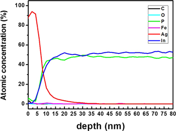
Figure 1. AES of InFeP:Ag.
Download figure:
Standard image High-resolution imageXPS measurement was carried out in order to investigate the incorporation of Ag and verify the local chemical bonding of Ag in InP:Fe. Figure 2 shows the XPS spectra measured after the doping of Ag into InP:Fe subsequent to the evaporation of Ag on the InP:Fe using an e-beam evaporator. Strong characteristic peaks are observed for Ag 3d, Ag 3p, In 3d, and In 3p for the InFeP:Ag samples. The InFeP:Ag sample revealed mainly In, P, and Ag peaks. The sample exhibited weak Ag 3p1, Ag 3p3, but dominant Ag 3d peaks from which the molar concentration was determined to be 3.2 at.%, as presented in figure 2. The peaks of O, C and Fe 2P3/2 faintly appeared. High-resolution XPS core-level spectra were also taken for the Ag 3d, In 3d, and P 2p regions. Figure 3 shows the cores for the InFeP:Ag. The peaks of typical binding energies are observed around 368 eV for Ag 3d5 and 374 eV for Ag3d3 in InFeP:Ag, as shown in figure 3(a), respectively. These results suggest that noble metal Ag dopants were essentially incorporated into InP: Fe. And also, the trend of the 20 nm milling sample AES and XPS results is similar to the trend of the 22 nm ion milling sample. Therefore, our study is focused on the experiments and analysis for the 22 nm ion milling sample. The In 3d core is spin–orbit split to 3d5/2 and 3d3/2 with peak positions at 444.1 and 453.6 eV in InFeP:Ag, respectively, as shown in figure 3(b). Figure 3(c) represents the XPS spectra of the P 2p core with peak positions at 128.4 eV corresponding to P from InP and at 133.2 eV corresponding to oxidized P species in InFeP:Ag. No shift was observed for any XPS spectra of In 3d and P 2p. This is in agreement with the values in standard spectra. The trend of the XPS results coincides with that of the AES results, especially Ag 3d5. The identity and formation of the InFeP:Ag nanorods will be demonstrated in more detail by TEM and XRD based on the AES and XPS results.
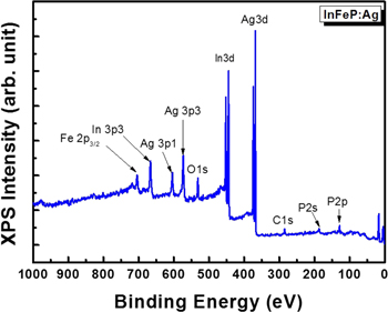
Figure 2. XPS spectra measured after the thermal annealing in InFeP:Ag.
Download figure:
Standard image High-resolution image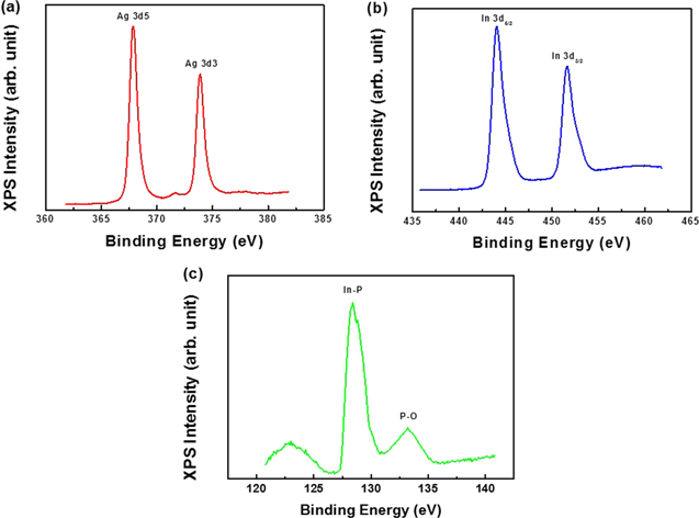
Figure 3. High-resolution XPS spectra for InFeP:Ag. (a) Ag 3d, (b) In 3d, and (c) P 2p.
Download figure:
Standard image High-resolution imageIn order to verify and investigate the formation of InFeP:Ag nanorods using an ion milling method, the cross-sectional TEM measurements were performed after ion milling for SI-InP:Fe without Ag deposition and for InFeP:Ag with Ag deposition, respectively. Because our investigation for InFeP:Ag nanorods was established using the milling method after deposition with noble metal Ag on SI-InP:Fe, cross-sectional TEM images of pure SI-InP:Fe after ion milling without Ag deposition were investigated in order to compare pure SI-InP:Fe with InFeP:Ag nanorods after ion milling. Figure 4 showed the total measurements for the cross-sectional TEM images of both pure InP:Fe and InFeP:Ag nanorods based on AES, where the injected Ag was diffused into InP:Fe without a change of stoichiometry, and XPS, which verified the local chemical bonding of Ag in InP:Fe [26]. Figures 4(a) and (b) show cross-sectional TEM images after ion milling of SI-InP:Fe without Ag deposition. The results of cross-sectional TEM images after 20 and 22 nm ion milling for SI-InP:Fe without Ag deposition showed the unclear and ambiguous formation of InP:Fe nanorods rather than nanorods precisely compared with InFeP:Ag nanorods as shown in figures 4(c) and (d). Figure 4(c) shows the cross-sectional TEM image of the InFeP:Ag nanorods after 20 nm ion milling subsequent to the deposition of Ag, compared with figure 4(a). The uniform and distinct nanorods were produced without Ag-related secondary phase and the average height was approximately 40 nm. Figure 4(d) shows the cross-sectional TEM image of the InFeP:Ag nanorods after 22 nm ion milling subsequent to the deposition of Ag, compared with figure 4(b). More uniform and distinct nanorods were produced, compared with figure 4(b) and the average height was 50 nm due to the increased ion milling. In addition, the density and height of the nanorods were simultaneously increased in comparison with figure 4(c). The nanorod features of InP:Fe were not completely clear regardless of the ion milling depth. However, the InFeP:Ag nanorods were clearly formed with increasing ion milling depth, compared with the unclear InP:Fe. These results were explicitly caused by the Ag deposition layer. The Ag layer plays a decisive role in the formation of the InFeP:Ag nanorods. As a result of annealing subsequent to the deposition of Ag on InP:Fe, most of the Ag was inner diffused and Ag partly existed on InP:Fe. The thickness of the residual Ag was approximately 7 nm, as can be seen in figure 4(e). Such results support with certainty that most of the Ag was inner diffused into the host material InP because the injected Ag was about 30 nm in depth in the AES measurement. Figure 4(e) shows the magnified cross-sectional TEM image for the InFeP:Ag single nanorod after 22 nm ion milling. The inset of figure 4(e) represents the selected area diffraction pattern from a single nanorod of InFeP:Ag, so as to examine the lattice structure. It is confirmed that the lattice is well aligned without distortion and that the nanorods are a single-crystalline zinc-blende structure.

Figure 4. Cross-sectional TEM images of the samples. Cross-sectional TEM image of InP:Fe without Ag layer after (a) 20 nm and (b) 22 nm ion milling, respectively. Magnified cross-sectional TEM image of InFeP:Ag single nanorods after (c) 20 nm and (d) 22 nm ion milling, respectively. (e) Magnified cross-sectional image of TEM for an InFeP:Ag single nanorod after 22 nm ion milling. Inset of figure 4(e) shows the selected area diffraction pattern from the InFeP:Ag single nanorod.
Download figure:
Standard image High-resolution imageIn order to support and demonstrate the above TEM results, the XRD measurements for the InFeP:Ag nanorods were carried out after 20 and 22 nm ion milling. Figure 5 represents the wide scan of the XRD spectrum for the InFeP:Ag nanorods after 22 nm ion milling involving 20 nm. It is clear from the reflections that the InFeP:Ag nanorods were uniformly grown and had good crystallinity without secondary phase (InAg and AgP, etc). Moreover, it is evident that the nanorods have a preferred InP structure with (002) orientation. From the XRD spectrum, the strong peaks near 2Ө = 30.44° according to the InP: Fe (002) crystal plane were obtained for InP: Fe together with the InFeP:Ag nanorods. This consequently indicates that the samples have a single-crystalline phase of intrinsic InFeP:Ag. The broad and weak peaks near 44.4° can be attributed to the (002) crystallinity of the Ag nanocrystal (Ag XRD Ref. No. 00-087-07-0719) [27]. These peaks are caused by the residual Ag, which agrees with the result of TEM analysis after ion milling. The strong and asymmetric peaks near at 2Ө = 30.44° occurred after 20 and 22 nm ion milling. In order to inspect the variation of FWHM for the InFeP:Ag nanorods due to the injection of Ag, we carried out double-crystal x-ray rocking curve (DCRC) measurements. Figure 5(b) showed the DCRC pattern of the InFeP:Ag nanorods after 20 and 22 nm ion milling. The shape of the main peak together with the shoulder peak around 74 arcsec revealed more asymmetric InFeP:Ag because of the injection of Ag. In addition, the variation in the FWHM of the InP (002) peaks agrees with the results of the TEM that the height and density of the InFeP:Ag nanorods increased. Here, it is noted that Ag2+ (ionic radius of 0.97 Å) must substitute for In (ionic radius of 0.81 Å) because the molar refractivity of an ion is proportional to the cube of its radius and acceptors that substitute for P have not been found in bulk InP [28]. The hump-shaped peak was caused by damage due to high 20 and 22 nm ion milling. Figure 5(c) shows the triple-axis diffraction (TAD) pattern of the InFeP:Ag nanorods after 20 and 22 nm ion milling. The FWHM of the TAD peaks was 29.95 and 30.29 arcsec and increased slightly after 20 and 22 nm ion milling, respectively. The shape of the peaks was faintly asymmetric and the FWHM was increased. The trend of the FWHM results coincides with the trend of the TEM results discussed in figure 4 that the InFeP:Ag nanorods are well formed according to ion milling depth. From the results and analysis, the formation direction of the nanorods was [200] without Ag-related secondary phases (InAg and AgP, etc), as shown by figure 4(e), namely by double cross-check. First and foremost, it is an essential point that big InFeP:Ag nanorods are commonly formed after 20 and 22 nm ion milling. There are decidedly different characteristics of InFeP:Ag in comparison with InZnP:Ag, as reported by our previous paper, although SI-InP:Fe is different to p-type InP:Zn.
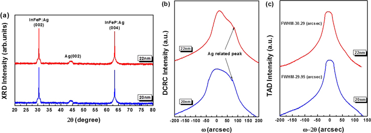
Figure 5. (a) Wide-scan XRD spectrum for the InFeP:Ag nanorods after 20 and 22 nm milling. (b) DCRC pattern of the InFeP:Ag nanorods after 20 and 22 nm milling. (c) Variation of FWHM for the TAD pattern of the InFeP:Ag nanorods after 20 and 22 nm ion milling.
Download figure:
Standard image High-resolution imageTogether with the formation of the InFeP:Ag nanorods, the magnetic properties of the InFeP:Ag nanorods were further investigated for various applications such as optical detectors, light-emitting diodes, and spintronics. Figure 6 showed the magnetic properties for InFeP:Ag nanorods using SQUID. In view of the TEM images for the InFeP:Ag nanorods (figures 4(c) and (d)), the measurements of the magnetic properties were representatively performed for the 22 nm ion milling sample. The magnetization versus magnetic field (M-H) and magnetization versus temperature (M-T) curves for cleaned InP:Fe substrates were recorded as having subtracted their diamagnetic contribution from the InFeP:Ag nanorods. This procedure ensures that the measured ferromagnetic phenomenon is that of the InFeP:Ag nanorods and not that of the substrate. Figure 6(a) presents the M-H curve for the InFeP:Ag nanorods after 22 nm ion milling measured at 10 K, using SQUID together with the InZnP:Ag nanorods, which we previously reported [23]. The remnant magnetization (Mr), and saturation magnetization (Ms) of the InFeP:Ag nanorods are 1.27 × 10⁻⁴ emu g−1 and 5.02 × 10⁻⁴ emu g−1, respectively. These magnetization values of the InFeP:Ag nanorods are approximately one order higher than that of the InZnP:Ag nanorods. In order to clarify and demonstrate the origin of the ferromagnetism, whether due to defect-related magnetism or not, the magnetic properties were measured according to ion milling depth. The InP:Fe without a Ag layer after 20 and 22 nm ion milling was non-magnetic, as shown in figure 6(b). This indicates that the magnetism of the InFeP:Ag nanorods originated from the interaction between InP:Fe and Ag. The magnetism is not produced by defect-related magnetism due to ion milling as evidenced by performing a double cross-check of XRD and TEM. Therefore, it is confirmed that the enhanced magnetism of the InFeP:Ag nanorods takes place clearly. The clear opening of the ferromagnetic hysteresis loop indicates the formation of ferromagnetic spin coupling interaction in InP:Fe doped with Ag. To trace the Curie temperature (Tc) of the InFeP:Ag nanorods, both field-cooled (FC) and zero-field-cooled (ZFC) magnetization measurements were carried out from 10–350 K. The M-T curves were measured under a magnetic field of 3000 and 0 Oe for FC and ZFC, respectively. Figure 6(c) represents the magnetization curves as a function of the temperature for the InFeP:Ag nanorods. The noticeable ferromagnetic signature of the InFeP:Ag nanorods was observed to persist up to around 350 K and no sudden drop in magnetization was observed as the temperature was increased to 350 K, indicating a Tc near 350 K, as can be seen in figure 6(c). We suggest that the absence of abrupt change in the ZFC curves rules out the existence of magnetic clusters [29], which is in line with the previous TEM and XRD analyses. Ferromagnetism observed from bulk and epilayer InMnP partly originated by cluster including Mn oxidation and intrinsic InMnP, which displays low Tc [6, 24, 30, 31]. In our case, the origin of the magnetism can be analyzed on the following basis under conditions mediated by holes supplied with TM, including noble metal Ag. Namely, our ferromagnetism is analyzed by the combination of material characteristics (InP:Fe and InP:Zn) with the RKKY model mediated with holes (p-d exchange interaction). In relation to material characteristics, the dopant of ∼1015 cm−3 was conventionally injected into the host materials, so as to make an SI compound semiconductor. In the case of SI-InP:Fe, Fe (concentration ∼ 1015) is injected into the InP compound semiconductor and p-type InP:Zn, and Zn (concentration ∼ 1018) is injected into the InP compound semiconductor. The difference in quantity between InP:Fe and InP:Zn is ∼103 cm−3, namely the dopant quantity of Fe is 103 cm−3 less than Zn. This fact means that the In cation site of InP:Fe is occupied by much more Ag in comparison with InP:Zn. Consequently, many more holes are produced from InFeP:Ag nanorods compared with InZnP:Ag nanorods. Actually, the M-H and M-T curves of the InFeP:Ag nanorods are strongly enhanced in comparison with the InZnP:Ag nanorods, as shown in figures 6(a) and (c). Generally, the process of ferromagnetic formation in III-V compound semiconductor doped with TM or ferromagnetic elements (Fe, Co, and Ni) is explained by the RKKY model mediated with holes (p-d exchange interaction) and mediated with electrons (s-d exchange interaction). In addition to analyses of the above material characteristics, the ferromagnetic theory related to conventional III-V compound semiconductor doped with TM is combined with the above material characteristics.

Figure 6. (a) M-H curves for InFeP:Ag nanorods after 22 nm ion milling measured at 10 K using SQUID together with InZnP:Ag nanorods, as previously reported [23]. (b) M-H curves of InP:Fe without an Ag layer after 20 and 22 nm ion milling. (c) FC and ZFC curves of InP:Fe nanorods after 22 nm ion milling.
Download figure:
Standard image High-resolution image
There are ferromagnetic types of Mn centers possibly formed in III-V compounds. Type I: the first type of neutral Mn center (A0) is substitutional  with the ground-state spin S = 2 and its related transition was found mainly in GaP:Mn [32]. Type II: the second type of neutral Mn center (A0) is [d4 core + e (tightly bound electron)] + h (weakly bound hole, binding energy = 0.113 eV in the case of GaAs:Mn) →
  with the ground-state total angular momentum J = 4 and has the properties of ferromagnetic semiconductors, and was found in some bulk GaAs:Mn and InP:Mn samples [33, 34]. Type III: the third type of Mn center is the ionized
  center (A−) with the ground-state spin S = 5/2, dissociation of holes from type II, and was found in GaP:Mn, GaAs:Mn bulks, and GaAs:Mn, InAs:Mn epilayers: i.e.
  + hv →
  + hole = A0 + hv → A− + hole. It is explained that the ferromagnetic InFeP:Ag is produced by the substitution of Ag into the In cation site. The substitution of Ag into In produced free hole and the ferromagnetic spin coupling, which is caused by the mediation by free holes, namely,
  = A0 →
  + hole → A− + hole. Anyway, the theory related to noble metal Ag will continue to develop the proper theory together with various experiments.
4. Conclusion
The fabrication of nanorods is achieved through deposition with noble metal Ag done using an e-beam evaporator and then ion milling of 20 and 22 nm. The AES results of InFeP:Ag indicated that the injected Ag was diffused into InP:Fe and was about 30 nm in depth. Strong characteristic peaks in the XPS spectra are observed for Ag 3d, Ag 3p, In 3d, and In 3p for the InFeP:Ag samples. The trend of results for XPS coincides with those of results for AES, especially Ag 3d5. TEM results revealed that the InFeP:Ag nanorods were clearly formed with increasing ion milling depth compared with the unclear InP:Fe. The Ag layer plays a decisive role in the formation of the InFeP:Ag nanorods. The variation of FWHM for DCRC and TAD peaks demonstrates that noble metal Ag is incorporated into the InFeP:Ag nanorods. From the XRD results and analysis, the formation direction of the nanorods was [200] without Ag-related secondary phases. It is an essential point that the formation of well-aligned InFeP:Ag nanorods is commonly produced after 20 and 22 nm ion milling. The clear opening of the ferromagnetic hysteresis loop and the absence of abrupt change in the ZFC curves indicate the formation of enhanced ferromagnetic spin coupling interaction in InP:Fe doped with Ag. The origin of the ferromagnetism in the InFeP:Ag nanorods can be explained by the combination of material characteristics (InP:Fe and InP:Zn) with the RKKY model mediated with hole (p-d exchange interaction). The substitution of Ag into In produced free hole and the ferromagnetic spin coupling is caused by the mediation by free holes. This study suggests that the InFeP:Ag nanorods should be a potential candidate for the application of spintronic devices.
Acknowledgments
This work was supported by the National Research Foundation of Korea (NRF) grant funded by the Ministry of Education, Science and Technology (MEST) (Nos. NRF-2017R1D1A1B03030964, 2016R1C1B1014103, 2016R1A6A1A03012877, 2016R1A2B4011706, 2014R1A2A1A12066298, 2015 R1D1A1A01060743, 2015R1A2A2A01004782, 2016R1D1A1B03932295) and the Quantum-functional Semiconductor Research Center (QSRC) of Dongguk University, and supported by the KIST institutional program.