

Abstract
A simple two-step CVD method is developed to realize the growth of high-quality tin-catalyzed CdSSe alloy nanowires. Microstructural characterizations demonstrate that these wires are high-quality crystalline nanostructures. Local photoluminescence investigation of these nanostructures shows a typical band edge emission at 656 nm with a full-width at half-maximum of 22.3 nm. Optical waveguide measurement along an individual nanowire indicates that the output signal of the guided light has a rapid linear decrease accompanied with maximum red-shift about 109 meV after the transmission of 102 μm. This obvious red-shift is caused by the intensive band-tail absorption during the optical transmission process. Moreover, optically pumped nanolasers are successfully realized at room temperature based on these unique wires, further demonstrating the achievement of stimulated emission from spontaneous emission, promoted by the pump power intensity. This work may find a simple route to the manufacture of superior nanowires for applications in waveguide and integrated photonic devices.
Export citation and abstract BibTeX RIS
Introduction
One-dimensional semiconductor nanostructures have received increasing attention in recent years due to their potential application in electronic and optoelectronic devices, including solar cells, photodetectors, nanoscale lasers, color displays and transistors [1–10]. Semiconductor nanowires (NWs), with nanoscale diameter and microscale length, can simultaneously function as both active gain materials and optical waveguide cavities, due to their high refractive index in contrast to surroundings [11–14], thus showing great promise for integrated photonic applications [15–18]. Nanoscale lasers have drawn a great deal of attention not only for their nanoscale and optical cavity effects [14], but also for their high-resolution and sensitivity applications in imaging [19], sensing [20], biological quantification [21] and photonics [22].
In recent years, various nanolasers have emerged and made great achievements in optical communication and photon transmission fields, including tunable nanolasers [12, 13, 23, 24], low-threshold nanolasers [25, 26] and multi-wavelength lasers [27, 28]. However, traditional semiconductor nanolasers still face challenges in large-scale application, caused by many constraints such as high cost, large size and integration difficulties [11, 14]. Furthermore, NW based waveguides show huge potential in future all-optical communications and full-color displays [29–31]. For example, Yang et al report super-long-SnO2-nanobelt based waveguides for sub-wavelength photonics applications [32]. Li et al report an all-optical waveguide based full-color display using several crossed trimethylene terephthalate nanofiber structures [33]. Pan et al report a color-tunable optical waveguide of CdS nanostructures with various doping content [34]. Additionally, the optical waveguide behavior of CdSe nanostructures has rarely been reported, owing to optical inactivity caused by the forbidden spin effect of angular momentum projection and transitions to the valence band [35, 36].
In light of this, high-quality crystallinity and ideal resonant cavities are essentially requirements for nanolasers [13, 37]. Chemical vapor deposition (CVD) [38–40] is introduced as an attractive approach for the growth of diverse NWs with the advantages of easy set-up, low-cost, mild operation and high yield. In particular, the CVD approach involving the evaporation of solid precursors has been particularly popular, because of its flexibility for a wide range of materials. This approach, however, is usually limited by its poor growth controllability, which has prevented its large-scale application in the growth of high-quality NWs. In this work, we develop a two-step CVD method with moving source to synthesize tin-cayalyzed CdSSe alloy NWs. Structural characterizations and optical investigations suggest that the wires produced have high-quality crystallinity, showing excellent band edge emission and transmission performance. Waveguide measurements of a single NW indicate that the guided light has a rapid linear decrease accompanied by an obvious red-shift of 109 meV after transmission at ∼102 μm. This notable red-shift is related to optical re-absorption effects during the optical transmissions, caused by local structural disorder in the nanostructures. Moreover, a high-quality 656 nm nanolaser has been successfully realized at room temperature based on these unique NWs. All these results evidently suggest a feasible CVD method, using moving precursors, to achieve superior nanostructures which may have potential applications in waveguide and integrated photonic devices.
Experimental procedure
The tin-catalyzed CdSSe alloy NWs are growth via a two-step CVD method with a moving source, as schematically shown in figure 1. A horizontal furnace (OTF-1200) with a quartz tube is used (length 180 cm, inner diameter 50 mm) here. At the beginning, an alumina boat loaded with pure tin powder (Alfa Aesar, 99.99%) is put inside the heating center of the chamber, while the other two boats, with CdSe and CdS powders (Alfa Aesar, 99.999%), respectively, are located far away from the heating zone, and separated by quartz rods. Several pieces of Si wafers are placed downstream to collect the product. High purity N2 (99.999%) is introduced into the tube at a rate of 120 sccm for 50 min, so as to purge the air from the chamber before the growth process. The temperature is then slowly rose to 800 °C, at a pressure of 300 mbar, as shown in step 1 in figure 1. After 10 min of growth, the boats with tin powder and CdS/CdSe sources are pushed respectively out of and into the heating zone, being driven by a step motor through magnetic force along the length direction. Then the temperature is elevated to 850 °C at a rate of 25 °C min−1 and kept for an additional 50 min, as shown in step 2 in figure 1. Finally, the furnace is naturally reduced to room temperature.
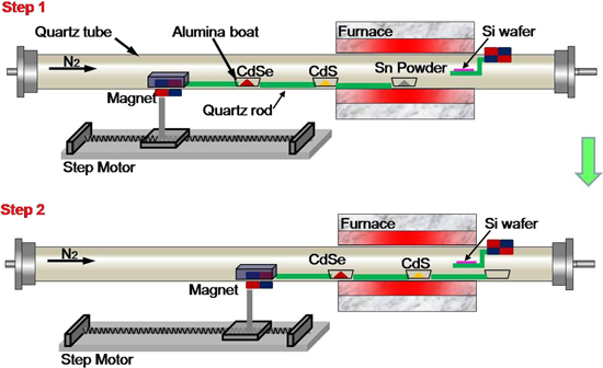
Figure 1. Schematic diagram of the CVD nanostructure synthesis system.
Download figure:
Standard image High-resolution imageThe optical waveguide and PL spectra of the NWs are measured through an optical microscope system. The 405 nm laser beam is focused and pumped on the NWs. The optical output signal is detected at the end of the wire by an Ocean Optics spectrometer (USB4000). The image is recorded by a charge-coupled device camera. The nanolaser from a single wire is optically pumped by a pulse laser beam at 355 nm. The output light is collected by a microscope objective lens (Nikon X20). Optical transport properties and stimulated emission investigation of these alloy CdSSe wires are studied in detail at room temperature.
Results and discussion
A typical scanning electron microscopy (SEM) image in figure 2(a) reveals the as-grown nanostructures are composed of NWs with a length of several tens of micrometers and diameter ranging from 80 nm to 400 nm. The catalyst is observed to be located at the tip of the NWs (inset of figure 1(a)), which indicates that these NWs are grown through the vapor−liquid−solid mechanism [25]. The energy dispersive x-ray (EDX) spectra from two typical positions along the axial direction of a wire are shown in figures 2(b) and (c), and reveal that position 1 is mainly composed of S, Cd, Se and Sn, while position 2 consists of S, Cd and Se. Two-dimensional elemental mapping of the selected area (figure 2(d)) from an individual wire is used to clearly display the element distribution, and suggests that Cd, S and Se are homogeneously distributed across the whole wire, while Sn is located at the tip of the wire, which is consistent with the EDX profile in figures 2(b) and (c). Microstructural investigation of these nanostructures is performed using transmission electron microscopy (TEM). Figure 2(e) displays the high-resolution TEM (HR-TEM) image and corresponding selected area electron diffraction pattern (SAED) of the wire, which indicates that the wire has clear lattice profiles without obvious defects, further indicating high-quality crystallinity with a wurtzite structure [13]. The measured plane spacing of a selected region is 0.696 nm, consistent with the (002) lattice spacing of wurtzite CdS1−xSex alloy with Se mole fraction x ≈ 0.78 [25]. According to the structural analysis, the wire is grown along the [001] direction, assisted by a tin catalyst.

Figure 2. Compositional analysis of tin-catalyzed CdSSe alloy NWs. (a) SEM image of some typical CdSSe alloy NWs with tin catalysts on the wire-tips. (b) The EDS elemental mapping images of a single CdSSe NW. (c) and (d) EDS profiles of two typical positions along a wire, as indicated in b. (e) A typical HR-TEM image of the NW. Inset: corresponding SEXD patterns of the NW.
Download figure:
Standard image High-resolution imageAdditionally, optical measurement through an optical microscope system is shown in figure 3. Figure 3(a) shows the schematic diagram of the experimental configuration for the measurement of the optical waveguide. Since the bandgap along the homogeneous NW is unchanged, when a 403 nm continuous wavelength (CW) laser is focused and excited at the center of the CdSSe NW, the guiding light will be actively guided toward the two opposite directions during the re-absorption and re-emitting process, as shown in figure 3(a). In this work, the waveguiding measurements are performed on these NWs without Sn catalysts (See figure 3(b)). The optical photograph (inset in figure 2(b)) and real color image (figure 2(b)) of the NW suggest a straight wire with good waveguide properties. Figures 3(c) and (d) exhibit the PL spectra of the excited (position E) and output (position R) positions of the NW, respectively. Notably, the PL spectrum at the exited position shows a PL peak at 656 nm with a full-width of half-maxmum (FWHM) about 22.3 nm, while the output signal has a PL peak at 671 nm with a FWHM about 17.6 nm. This interesting red-shift will be systematically investigated in this paper, which may result from band-tail absorption during the absorption–emission–absorption process [41]. It is worth noting that some nanostructures with needle morphology are produced at the high temperature region, as shown in figure S1 (supporting information—available online at stacks.iop.org/NANO/29/185201/mmedia). in situ PL spectra of the CdSSe alloy NW and needle-like nanostructure from the excited position indicate that they have the same emission peak at 656 nm, as shown in figures S1(b)–(e) (supporting information).
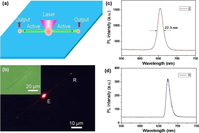
Figure 3. (a) Schematic diagram of waveguiding measurement with local excitation at the center of the CdSSe alloy NW. (b) Real color image of an individual tin-catalyzed CdSSe alloy NW, which was dispersed on a MgF2 substrate for optical measurement. Inset: corresponding optical image of the wire. (c) in situ PL spectrum from the excited position pumped by a 403 nm laser beam. (d) PL spectrum from the output side (position R).
Download figure:
Standard image High-resolution imageTo shed light on their optical waveguide properties, figure 4 gives a systematic overview of waveguide measurements using an individual NW with diameter of 90 nm and length of 120 μm. As can be seen, figure 4(a) shows a typical real color image of a CdSSe NW illuminated by a 403 nm unfocused laser, which exhibits a homogeneous red emission along the whole wire. Figure 4(b) exhibits a series of dark field PL images of a single alloy CdSSe NW excited at different positions along the length. Figures 4(c) and (d) depict the in situ PL spectra and output signals of the NW corresponding to figure 4(b). As we can see, the position-dependent PL spectra (O1−O5) have nearly the same intensity, while the PL intensity and wavelength of the output signals (P1−P5) are totally different after the light transmission. As can be seen, the output signals (P1−P5) exhibit broad spontaneous emission bands at low pumping power density. Some resonance peaks are observed at both sides (See figure 3(b)) of the band edge emission, owing to the optical resonances in the cavity [42–49]. Further investigations are needed to explain this result. Notably, the output spectra show obvious red-shift depending on the increase of the propagation distance, which may be due to the energy loss in the repeated absorption–emission–absorption process during light transport along the wires [41]. This process of photon re-absorption and re-emission with lower energy proceeds many times, causing a red-shift of the PL band with continual loss of energy. Figure 4(e) shows the propagation-distance-dependent PL intensity of the output signals, which exhibits a near-linear decrease. This can be attributed to the self-absorption process of the guided light. Figure 4(f) gives the propagation-length-dependent red-shift of the output PL spectra. The guided light has an increased red-shift of ∼80 meV after transmission through about 40 μm, while the energy loss of the guided light is restricted when the propagation distance is beyond 40 μm, and the red-shift reaches a maximum of ∼104 meV after transmission through 100 μm. All these results indicate that these tin-catalyzed alloy NWs are good candidates for nanoscale lasers owing to their natural Fabry–Perot (F-P) cavities and gain materials.

Figure 4. Optical waveguide properties of a typical tin-catalyzed CdSSe NW. (a) Real color photographs of an individual CdSSe alloy NW illuminated by an unfocused 403 nm laser (scale bar is 20 μm). (b) A series of real color images of the CdSSe NW t locally excited at various regions by a 403 nm laser beam. (c), (d) PL spectra at the excitation position (O1-O5) and output ends (P1-P5) of the NW, respectively (Integration time is 0.2 s in the detection). (e) Propagation-distance-dependent PL intensity of the guided light. (f) Propagation-distance-dependent spectral red-shift of the output signals of the guided light. The propagation distance is measured from the excitation spot (O1−5) to the wire end (P1−5).
Download figure:
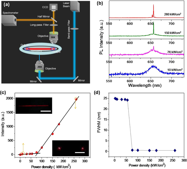
Standard image High-resolution imageGenerally, when the laser oscillation is take place within a single NW, the round-trip gain should compensate the round-trip loss [50]. Here, a 355 nm pulse laser is used to pump the alloy NWs as schematically shown in figure 5(a). The laser spot size is focused to 80 μm by a Nikon X20 Len. The wire is transferred to the MgF2 substrate and totally excited by the laser beam. Figure 5(b) shows the power dependent PL spectra of the NW. As can be seen, when the pumping power is below the threshold, an emission peak appears at 656 nm, which is owing to the band-to-band transition. A 656.2 nm line becomes apparent at the high energy side when the power density is above the threshold. Notably, the line width of the laser peak is calculated as 0.48 nm, which is much narrower than the spontaneous emission peak (∼22.3 nm). The Q factor is an important parameter to describe a laser cavity. Here, the nanolaser Q factor is calculated to be about 1366, suggesting a high-quality nanoscale laser. Figure 5(c) depicts the power-density-dependent PL intensity curve of the wire. This nonlinear response of the NW-laser shows a threshold about 76 kW cm−2 as a kink between the two linear regions of the spontaneous and stimulated emissions. Left and right insets show two typical real color emission images of the wires below and above the laser threshold, respectively. Figure S2 shows the room temperature time-resolved PL spectra of Sn-catalyzed CdSSe NW when the excitation fluence is below (12 kW cm−2, red line) and above (180 kW cm−2, blue line) the lasing threshold (see supporting information). The calculated lifetimes for the spontaneous and stimulated emissions are 1.87 ns and 0.16 ns, respectively. The time-resolved PL measurements further prove the occurrence of lasing in the NW F-P cavities. Consistent with the lasing emissions spectra in figure 5(b), two strong lasing spots located at both ends of the wire are clearly observed in the right inset of figure 5(c). Figure 5(d) shows the pumping-power-dependent FWHM of a typical CdSSe NW. As can been seen, when the pump power passes the threshold, the FWHM decreases from 23 nm to 0.48 nm, indicating a transformation from spontaneous emission to stimulated emission.
Figure 5. Optical investigation of a single CdSSe wire. (a) Schematic diagram of the optical set-up for the PL measurement. (b) Pumping-power-dependent PL spectra of a typical wire illuminated by a 355 nm pulse laser beam; blue for 10 kW cm−2, rose for 76 kW cm−2, green for 150 kW cm−2 and red for 260 kW cm−2. (c) Nonlinear response of the NW-laser output power with increased pumping power, showing a laser threshold of 76 kW cm−2 as a kink between the two linear regions of spontaneous and stimulated emission. The top and lower insets show real color images of spontaneous emission and stimulated emission, at pump powers of 10 kW cm−2 and 260 kW cm−2, respectively (scale bar is 10 μm). (d) Pumping-power-dependent FWHM of a typical CdSSe NW.
Download figure:
Standard image High-resolution image
Conclusions
Here we report a simple two-step CVD method to realize high-quality tin-catalyzed CdSSe nanostructures. Structural characterization indicates that the wires are grown along the axial direction, catalyzed by tin catalysts at their tips. Optical waveguide measurements of these wires show linear decrease and obvious red-shift after the optical transmission, caused by the intensive absorption–emission–absorption process during light transport. Moreover, room temperature optically pumped lasing has been realized based on these unique NWs, further demonstrating the achievement of transition from spontaneous emission to stimulated emission. It is anticipated that the present work can provide extendable availability for tin-catalyzed high-quality low-dimensional nanostructures to construct high-performance optoelectronic devices.
Notes
The authors declare no competing financial interest.
Acknowledgments
This work was financially supported by the National Natural Science Foundation of China (Nos. 51602276, 61574122, 61571386, 11604280), the Key Research Program in the College of Henan Province (No. 17A140028), the Science and Technology Project of Henan Province (No. 172102210458), and the Nan Hu Young Scholar Supporting Program of XYNU.