

Abstract
The optical confinement and strong carrier coupling within a semiconductor nanostructure cavity are crucial for the modulation of emission properties. Fundamental understanding of the light–matter interaction in a low dimensional system is important. In this paper, we synthesized high-quality hexagonal Te-doped CdS nanowires by two-step chemical vapor deposition and investigated systematically the doping concentration, temperature, excitation power, excitation wavelength dependent Raman, photoluminescence and carrier lifetime decay. Scanning electron microscopy, energy dispersive x-ray spectrometry and x-ray diffraction confirmed Te-doping in the as-prepared samples. The strong surface optical (SO) phonon mode is observed in the micro-Raman spectra of an individual Te–CdS nanowire, which is unsuitable in large-sized structures. In situ micro-photoluminescence (μ-PL) characterization shows dominant confined defect state emission with whispering gallery mode (WGM) characteristics. The emission peak position shifts under increased excitation power, demonstrating the inelastic scattering by bound carriers. In addition, the short wavelength emission modes are dominant at a low temperature (80 K) while the long wavelength emission modes are dominant at a high temperature (300 K) due to different recombination processes contributing to the WGM resonant bands, which was also confirmed by the time-resolved PL measurement. All these results reflect strong coupling between the surface evanescent-wave in the WGM cavity and the SO phonon/polaron, which will facilitate the rational tailoring of surface/interface relevant properties for nanophotonic device applications.
Export citation and abstract BibTeX RIS
Introduction
As a result of the low dimensionality and native optical resonator, one-dimensional (1D) semiconductor nanostructures offer a critical platform to study the confined coherent transport of phonons, photons, electrons, excitons and polarons etc along a definite direction. Recently, 1D nanostructures have demonstrated many novel light emission/waveguide properties and should find extensive potential applications in integrated photonics/optoelectronics systems [1, 2]. There are two important optical cavities: Fabry–Pérot (FP) and whispering gallery mode (WGM), in 1D nanostructures. These micro-cavity related unique photonic/optoelectronic properties, such as: multi-cavity integration and multi-mode modulation emission/lasing, have drawn considerable attention for many years [3, 4]. Compared with a FP cavity, a WGM cavity can confine and store more photons or energy within the small volume of nanostructures. Therefore, strong light–matter interactions in WGM exhibit larger optical density and carrier confinement emanating a higher quality factor (Q). Furthermore, the evanescent-wave existing at the WGM cavity boundary is very sensitive to external surface perturbation or surrounding medium, which can effectively change the optical transport path inside and results in shifted resonant emission peaks [5–7].
The optical properties of 1D nanostructures can be modulated further by phase structure, composition, morphology, heterostructure and doping [8–11]. Specifically, the doping technique applied by the chemical vapor deposition (CVD) method is an efficient process widely used to tune the optical properties of nanostructures. The minor amount of dopant modifies the electrical and optical properties greatly while maintaining the matrix-crystal structure. For example, as an important member of the II–VI group, pure and doped CdS nanostructures have been synthesized and demonstrated distinct photoluminescence (PL) [12]. In contrast to prevalent Se-doping CdS, which favors the formation of a uniform CdSxSe1−x alloy due to the similar hexagonal crystal structures of CdS and CdSe [13, 14], the other chalcogenic elements, such as O and Te, may produce a separated phase structure during doping of CdS because of the different crystal structures of CdS (hexagonal) and CdO (rocksalt)/CdTe (cubic) [15, 16]. For example, we synthesized CdS@CdO core–shell microwires recently, instead of a uniform CdOxS1−x alloy, with the incorporation of a high oxygen concentration [17]. The novel PL from these CdS@CdO core–shell structures stimulated further research on the effect of Te-doping. Heavy Te-doping can cause more serious bond distortion and significant structural relaxation than that of O-doping, and consequently have a significant impact on electronic structure and surface-related physical properties. However, there are few reports on the synthesis of Te–CdS nanowires and their corresponding surface/emission properties[18].
Generally it is hard to observe surface dominant phenomena, such as the surface optical (SO) phonon mode, in large-sized nanowires due to the low surface ratio [19, 20]. In fact, the SO mode can be interpreted in terms of the Fröhlich mode, which is related to phonon confinement and bond distortion induced by significant structural relaxation and is dependent on the nanostructure's shape as well as the dopant concentration and dielectric constant of the surrounding material [21]. The SO mode offers numerous possibilities for studying exciting physical phenomena arising from carrier confinement or a large surface-to-volume ratio. Taking into consideration the SO confinement carrier and the WGM cavity, these will produce novel emission properties and light–matter interaction, which have not yet been studied in depth. In this regard, we synthesized Te–CdS nanowires via s two-step high-temperature thermal evaporation and deposition process. The morphology, chemical composition and crystallographic structure of the as-prepared product were examined by x-ray diffraction (XRD), scanning electron microscopy (SEM) and energy dispersive x-ray spectrometry (EDS). The emission property was measured under different laser excitation wavelengths/power, different temperatures and dopant concentrations. The PL spectra demonstrated strong WGM cavity characteristics while the Raman spectra showed evident SO scattering. These results represent interesting surface phonon/polaron confinement coupling and a strong light–matter interaction in the Te–CdS nanowires, which will push the development of multi-functional integration nanophotonic devices and may find important applications in optoelectronic systems.
Experimental details
A simple two-step growth technique based on magnetic force assistant substitution source material was used to synthesize the Te–CdS nanowires. The detailed experiment setup can be seen in reference [22]. The typical synthesis process was as follows: in the first step, one quartz boat containing a powder mixture of 0.2 g CdS and 0.2 g Sn and another quartz boat containing 0.1 g ZnTe powder were placed into a 1.5 m long quartz tube. Then the quartz tube was loaded into the tube furnace (Thermo Scientific-TF55035C) ensuring that the CdS and Sn powder was in the central region while the ZnTe powder was outside of the furnace. The central temperature was set to be 1000 °C. Before the reaction, high-purity Ar(90%)/H2(10%) was injected into the quartz tube with a constant flow rate of 100 SCCM (standard cubic centimeter per minute) to eliminate the O2 inside. After 2 h, the furnace was heated to 1000 °C at a rate of 28 °C min−1 and this was maintained at that temperature for 60 min. The CdS and Sn powder mixture was evaporated completely while the ZnTe powder was not at all evaporated during the first step. In the following step, keeping the furnace at 1000 °C, the ZnTe powder was put into the central temperature zone quickly and maintained for 40 min without changing any of the other experimental conditions. Finally, the furnace cooled down naturally to room temperature and the inner wall of the quartz tube at the temperature of 450–550 °C was covered with a layer of yellowish product, which was collected carefully for further characterization.
The size and morphology of the as-synthesized product were characterized by SEM (NovaSEM-450). The chemical composition was analyzed by EDS (Oxford X-max 20). The crystallographic phase structure was determined by XRD (Bruker D8 Advance). The Raman and steady PL spectra were measured by a high resolution Raman spectrometer (LabRAM HR Evolution, Horiba JY) using a continuous wave laser with wavelengths of 355 nm, 532 nm and 632.8 nm as the excitation light source. The PL lifetime decay profile was recorded by the time correlated single photon counting system (Picoquant 'Timeharp 300'). The picosecond pulsed laser diode with a wavelength of 375 nm (Picoquant 'PDL 800-B', 10–80 MHz) was used as the excitation source. A Linkam THMS600 and liquid nitrogen were used to cool the sample for temperature dependent measurements. In all the optical measurements, the excitation signal illuminated perpendicularly onto the sample surface and the Raman/PL was collected in situ.
Results and discussion
XRD was used to determine the phase structure of the as-prepared samples and the result is shown in figure 1(a). This pattern is in good agreement with the wurtzite CdS crystals (JCPDS card: 41-1049) with lattice constants of a = 4.141 Å and c = 6.720 Å. Hence, the as-synthesized product can be designated to wurtzite CdS. These strong and sharp diffraction peaks show high crystal quality of the as-prepared product. In addition, the diffraction peaks of Sn (JCPDS card: 4-673 for tetragonal with lattice constants of a = 5.831 Å and c = 3.182 Å) were clearly observed, indicating there were Sn particles existing on the CdS nanowires during the growth process. Its weak peak intensity indicates that the amount of Sn was less than CdS. Figure 1(b) shows enlarged diffraction peaks of (100), (002) and (101), which shift a little to a lower angle direction when compared to standard CdS. Doping can change the lattice constant [23]. Therefore, the present measurable shift of the diffraction peaks comes from the doped-Te because Te has a larger atomic radius than S. That is to say, Te can efficiently diffuse and substitute S in the CdS lattice under the growth conditions described in this paper. The doped-Te content was further confirmed by EDS.
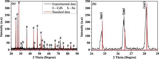
Figure 1. (a) XRD pattern of as-prepared product. (b) Enlarged diffraction peaks of (100), (002) and (101).
Download figure:
Standard image High-resolution imageFigures 2(a) and (b) show the morphology images of Te–CdS with low and high magnification, respectively, and show a uniform and smooth surface. The diameter ranged from 200 nm to 2 μm and the length ranged up to hundreds of micrometers. More importantly, the high magnification SEM revealed a hexagonal cross section (figure 2(e)), which was consistent with the XRD results and favors the formation of a WGM cavity [24]. We also observed a big ball at the nanowire tip. The EDS analysis indicated that the wire was dominantly CdS (figure 2(c)) while the ball was Sn (figure 2(d)). There was a little Te content in the nanowire, indicating effective doping and further confirming the XRD data. We further executed element mapping to detect the element distribution (figures 2(e)–(h)), which showed uniform distribution of Cd, S and Te along the nanowire length. It is notable that we did not use any substrate covered with Au thin film to collect the product. According to the SEM and EDS results, we propose that Sn was responsible for the nanowires' growth. This is similar to comb-like CdS growth by using a powder mixture of SnO2 and CdS as the source material [25]. Therefore, the Te–CdS nanowires obeyed the vapor–liquid–solid growth mechanism [26, 27]. In this case, Sn, instead of common Au, acted as the catalyst. It is known that Sn powder exists in the form of vapor at high temperatures due to its low melting point (232 °C). The vapor was then transported to the low temperature zone by carrier gas and deposited as small liquid droplets. The CdS powder also formed CdS vapor and was transported to the low temperature zone. This CdS vapor was absorbed preferentially on the pre-existing Sn droplets to form a Sn/CdS alloy. Once the concentration of absorbed CdS reached supersaturation, the CdS crystals precipitated from the catalyst interface. Therefore, the Sn catalyst particles or droplets acted as effective nucleation sites and were responsible for the growth of the CdS nanowires. Maintaining this growth process without changing the conditions will obtain long nanowires as long as the alloy droplets keep collecting the CdS vapor. After the growth of the CdS nanowires in the first step, we pushed the ZnTe powder into the central temperature zone to obtain ZnTe, Te and Zn vapor for reaction with the as-prepared CdS nanowires. Only a small amount of S was substituted by Te to form Tes [28]. In fact, only a small quantity of ZnTe powder evaporated.
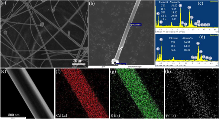
Figure 2. (a), (b) SEM of Te–CdS nanowires under low and high magnification, respectively. (c), (d) EDS of the nanowire backbone and the ball at the tip. (e)–(h) SEM image and corresponding Cd, S, Te element mapping.
Download figure:
Standard image High-resolution imageAs a non-destructive and non-contacting characterization method, Raman spectroscopy is extensively applied in low dimensional systems and provides valuable information about structural properties. We measured the Raman spectra of a single Te–CdS nanowire from 300 K to 80 K. As can be seen in figure 3(a), there were seven evident Raman scattering modes in the spectra, in which the 523 cm−1 mode came from the Si substrate. The two strong peaks at 302 and 600 cm−1 were assigned to be 1LO and 2LO of the wurtzite CdS crystal, which were polarized in the Z axis and strongly coupled with the electron or exciton transport along the c axis. The strength of the electron–phonon coupling in the semiconductors can be assessed by the intensity ratio of overtone phonons to fundamental phonons ( ) [29]. In our results, we obtained a large intensity ratio of
  (0.36), which reflects the enhanced electron–LO phonon coupling in the Te–CdS nanowires. The narrow full width at half-maximum (FWHM), around 12 cm−1, indicated the high crystalline quality of the Te–CdS nanowires.
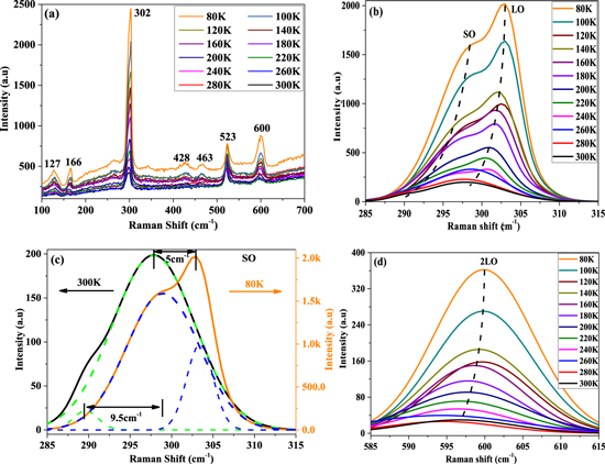
Figure 3. (a) Temperature dependent Raman spectra of a single Te–CdS nanowire under excitation of 532 nm laser. (b) Enlarged Raman spectra from (a) in the 285 ∼ 315 cm−1 range. (c) Extraction of the data at 300 K and 80 K for comparison. The green and blue dashed lines are fitted curves of 300 K and 80 K. (d) Enlarged Raman spectra from (a) in the 585 ∼ 615 cm−1 range (2LO mode). These black dashed lines in (b) and (d) are to guide the eye.
Download figure:
Standard image High-resolution imageThere were four others phonon modes (127, 166, 428 and 463 cm−1) with weak intensities observed in the Raman spectra, which were not the intrinsic phonon modes of CdS. The two modes 127 and 166 cm−1 were designated to the LO mode of the Te–Te bond and Cd–Te bond with A1 symmetry [30]. This is reasonable because a definite amount of Te substitution doping can form Cd–Te and Te–Te bonds in CdS nanowires, resulting in great modification of the optical properties. Another two peaks at 428 and 463 cm−1 cannot match any vibration mode of CdS, CdTe and Te. We observed that the 428 cm−1 peak was consistent with 302 cm−1 + 167 cm−1 while the 463 cm−1 peak was consistent with 302 cm−1 + 166 cm−1, so the 428 and 463 cm−1 peaks may have been the combination of the CdS LO mode with Te–Te and Cd–Te, respectively [31]. Such assembling, similar to the 2LO mode of CdS, reflects the enhanced electron–phonon interaction and strong coupling between doped-Te and the CdS matrix, providing a good mixture of Cd–S and Cd–Te bonds and more proof of the dopant Te entering the CdS lattice.
We further examined the Raman spectra by enlarging the 1LO and 2LO modes of CdS. Figure 3(b) is the Raman spectra in the range of 285 ∼ 315 cm−1. It is surprising that there was another peak position at the low frequency side of the LO phonon mode. According to the theory of Scott J F et al, we attributed this shoulder peak to scattering from the SO phonon [32]. A simple mathematical expression of the surface modes at 300 K is given in the case of an infinite cylinder or slab-type geometry: ωs = ωLO[ε∞(1 + ε0)/ε0(1 + ε∞)1/2, where ε0 and ε∞ are the dc and high frequency dielectric constants, respectively, while ωLO and ωs are the longitudinal and SO phonon frequencies, respectively [32]. By adopting ε∞ = 5.32, ε0 = 8.42 and ωLO = 298 cm−1 (the measurement values), we calculate the CdS surface mode frequency ωLO = 289 cm−1, which is in excellent agreement with the data shown in figure 3(c). The position of SO depends on the dielectric constant of the medium that is surrounding the wires as well as the temperature. Although both the LO and SO mode shifted to higher wavenumbers with the temperature decreasing from 300 K to 80 K (figure 3(b)), the shift distance of the SO mode (9.5 cm−1) was larger than that of the LO mode (5 cm−1), see the two fitting curves in figure 3(c), indicating more sensitivity to the temperature of the SO mode. This observable SO mode is surprising because it can only be detected in CdS nanoparticles with a size less than 3 nm [33]. In our sample, this size was too large to produce a large surface-to-volume ratio. So the SO mode may have been related to surface lattice deformation potential oscillation and momentum conservation constraint relaxation due to Te doping, both of which can supply strong Fourier components and absorb phonon momentum effectively. The evanescent-wave and polarons at the interface/surface also had an important contribution to the detected SO mode. Regarding the 2LO mode, we could not observe an evident shoulder mode at a low wavenumber. But the FWHM of 2LO was wider than that of 1LO + SO, which may indicate the presence of the 2SO-related mode but this cannot be resolved due to the instrument resolution restriction.
PL measurement is a very powerful characterization tool for the determination of the structure, surface, defect and impurity of semiconductor nanostructures. The PL can be modified by introducing a dopant because it has considerable influence on the deformation potential and photon–phonon coupling coefficient. We measured the PL spectra of a single Te–CdS nanowire under different excitation powers and temperatures. The emission was strong even under a low excitation power at room temperature. We could not observe any signal from the bandgap or exciton emission in all the spectra (figure 4(a)) due to the effect of the large amount of surface defect states. However, there were several oscillation modulation enhancement emission bands with a wide spectral range from 560 nm to 820 nm superposition on the background broad band (centered at 680 nm). Because these spectra were collected in situ, we excluded those with multi-mode emission peaks originating from the FP cavity along the longitudinal direction, which were usually emitted at the end facet. The emission could also transport and reflect perpendicularly between the top and bottom facet. We calculated the cavity length by using the formula: L = λ1λ2/[2n(λ1 − λ2)], where λ1, λ2 are the wavelengths of adjacent bands and n is the refractive index [34]. The calculated length was about 3 μm, which was larger than the perpendicular facet distance (800 nm) determined by SEM. Therefore, the perpendicular FP cavity was also excluded for its contribution to the multi-mode emission. From the emission spectral profiles in figure 4(a), WGM was the most possible cavity responsible for the multi-mode emission [17, 35]. When the nanowire was excited, the dominant trapped defect state due to Te incorporation emitted light far below the bandgap (background broad band), in which a large number of photons with varied wavelengths propagated along the surface boundary and some of them resonated to produce strong emission bands. This WGM multi-mode emission is entirely different from recent Te–CdS nanowires, showing only a broad defect band centered at 737 nm [18]. Therefore, this novel phenomenon deserves to be studied in detail. We excited the single nanowire under increasing laser power and the intensity of these modes increased greatly while the spectra profile remained almost unchanged. The enlarged spectra range of the single peak was extracted to find more information (figure 4(b)), from which an evident red shift of the peak under increasing excitation power was observed. In addition, the adjacent mode spacing increased from the high energy to the low energy region due to the reduced mode density of the long wavelength [36]. These two phenomena are contradictory with classic WGM resonators, where temperature and excitation power have little contribution to the WGM band energy. There must be an inelastic scattering process in the localized cavity photon responsible for the peak's continuous red shift. In the Raman spectra, we found that there was a strong electron–phonon interaction and surface phonon/polaron localization in the Te–CdS nanowires. At increasing excitation power, enhancement in the oscillator strength increased the bound excitons' density and improved carrier–phonon coupling, more localized carriers may have relaxed by emitting one or more SO phonons. The relaxation could improve the population of the low energy carrier and then may undergo further acceleration after the long transportation distance and assistance of the LO phonon. It was the surface carrier confinement and relaxation effect out of the varied local carrier density, combined with the evanescent-wave surface emission nature of the WGM cavity, which was responsible for the wavelength shift. The increased scattering among the confinement carriers is expected to decrease the oscillator strength of exciton transition [37], which is consistent with the absence of near bandgap/exciton emission in the PL spectra. This situation is different from the wavelength blue shift of near bandgap emission in ZnO nanowires under increased excitation power due to the FP cavity and exciton–polariton coupling [38].
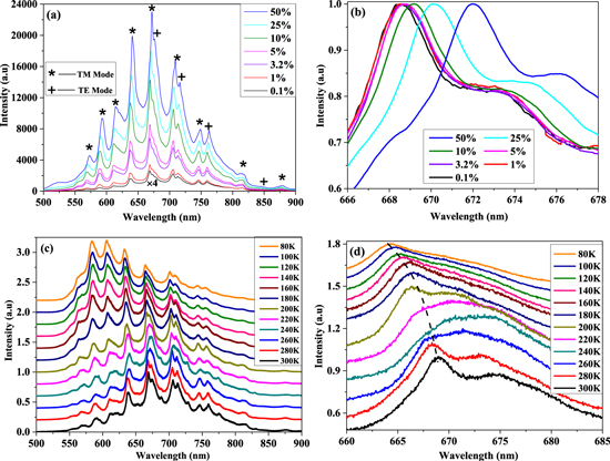
Figure 4. (a) PL spectra of a single Te–CdS nanowire under excitation of 355 nm laser with normalized excitation power of 0.5, 0.25, 0.1, 0.05, 0.032 and 0.001. (c) Normalized PL spectra of a single Te–CdS nanowire at temperatures ranging from 300 K to 80 K. (b) and (d) are correspond to normalized enlarged spectra.
Download figure:
Standard image High-resolution imageWe investigated further the effect of different temperatures on the PL spectra of a single Te–CdS nanowire. In figure 4(c), the peak position and number of all cavity modes almost remained the same at different temperature ranges. However, the enlarged PL spectra (figure 4(d)) shows that all peak positions shifted slightly, instead of having stable cavity mode characteristics. This abnormal phenomenon may have been due to the reduced light–matter interaction as well as confinement coupling of the phonon number, which then resulted in a higher population state of the high energy carrier. More importantly, we note the strongest mode shift from 668 nm to 583 nm when the temperature changed from 300 K to 80 K. That is, the short wavelength emission modes were dominant at low temperatures (80 K) while the long wavelength emission modes were dominant at high temperatures (300 K). This change clearly reflected the lattice temperature effect on the emission component of the different wavelengths. The large surface phonon at high temperatures could strongly couple carriers, leading to a low energy carrier population, and vice versa. Both the high gain of the short wavelength due to its large mode density and the high cavity loss was because of its limited confinement for long wavelength modes contributing to this phenomenon [39]. This interesting peak shift demonstrates the change in the local refractive index, optical dispersion and surface light propagation, which can find applications in slow light devices and evanescent-wave sensors [40].
There may be different origins for the WGM mode bands to the above discussion. We executed the PL lifetime measurement of all multi-mode emission bands to understand their recombination process. The typical time-resolved PL at room temperature is shown in figure 5(a). The different emission bands have different lifetime decays, which cause confusion since all of them were WGM modes in the same cavity, and they should have had the same decay time. We fit these decay curves by using the bi-exponential function expressed as the following: I(t) = A1exp(−t/τ1) + A2 exp(−t/τ2), where Α1 and A2 are the amplitudes and τ1 and τ2 are the short and long decay times, respectively [41]. The short lifetime τ1 is ascribed to the delocalized carrier recombination process while the long lifetime τ2 should correspond to surface localized carriers by phonon confinement [42, 43]. All the data Α1, A2, τ1, τ2 are summarized in table 1, from which we can see clearly the reduced lifetime with a shorter emission wavelength due to the larger confined carrier mode density and quenching effect. This large mode density is proved by the decreasing PL peak spacing from the low energy to high energy range (figure 4(a)). When the temperature decreased from 300 K to 200 K, the difference in the decay curves between all bands reduced greatly (figure 5(b)). These decay curves approach superposition and all the lifetime parameters increased at 100 K (figure 5(c)). The reduced quench effect contributed to the increased PL intensity (figure 4(c)) and long lifetime of the short wavelength, meaning all bands had almost the same lifetime parameters. The temperature dependent short and long lifetimes demonstrated a decreased recombination rate via thermally activated phonons at low temperatures. Therefore, the confined surface carrier coupling played an important role in these recombination processes and may be used to fabricate emerging topological insulator lasers [44, 45].
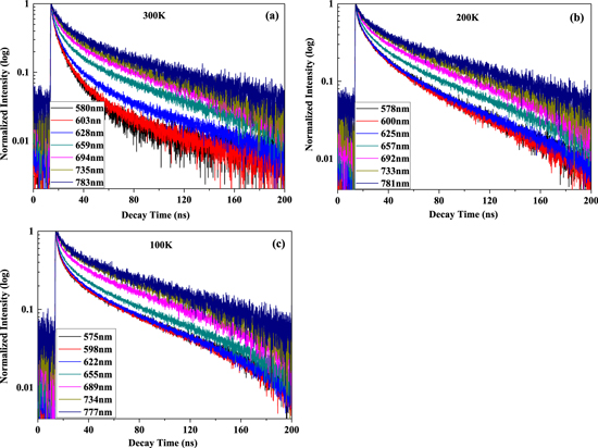
Figure 5. PL lifetime profiles of a single Te–CdS nanowire with picosecond 375 nm laser diode excitation under different temperatures: (a) 300 K; (b) 200 K; (c) 100 K.
Download figure:
Standard image High-resolution imageTable 1. The decay constants and amplitudes of all emission bands at different temperatures.
| 580 nm | 603 nm | 628 nm | 659 nm | 694 nm | 735 nm | 783 nm | ||
|---|---|---|---|---|---|---|---|---|
| A1 | 300 K | 0.2498 | 0.2071 | 0.2336 | 0.3250 | 0.4028 | 0.4230 | 0.4654 |
| 200 K | 0.4072 | 0.3881 | 0.3890 | 0.4390 | 0.5014 | 0.5332 | 0.5422 | |
| 100 K | 0.3964 | 0.4115 | 0.4013 | 0.4369 | 0.5178 | 0.5620 | 0.5786 | |
| A2 | 300 K | 0.7502 | 0.7929 | 0.7664 | 0.6750 | 0.5972 | 0.5770 | 0.5346 |
| 200 K | 0.3964 | 0.4115 | 0.4013 | 0.4369 | 0.5178 | 0.5620 | 0.5786 | |
| 100 K | 0.6036 | 0.5885 | 0.5987 | 0.5631 | 0.4822 | 0.4380 | 0.4214 | |
| τ1(ns) | 300 K | 22.02 | 29.15 | 39.79 | 50.02 | 55.6 | 60.67 | 60.1 |
| 200 K | 46.7 | 44.89 | 47.29 | 55.66 | 63.65 | 68.91 | 78.5 | |
| 100 K | 57.18 | 57.06 | 55.62 | 61.26 | 75.2 | 83 | 84.2 | |
| τ2(ns) | 300 K | 4.60 | 4.97 | 5.688 | 6.59 | 7.55 | 8.31 | 8.7 |
| 200 K | 7.85 | 7.46 | 7.47 | 7.8 | 8.3 | 8.69 | 10.27 | |
| 100 K | 5.93 | 5.93 | 6.34 | 6.59 | 8.21 | 9.2 | 9.41 |
In figure 5(c), there also occurred an anomalous bulge after 160 ns for some band decay, indicating the state propagation and reabsorption processes around 689 nm, 622 nm, and 655 nm at the low temperatures. This phenomenon was absent at room temperature for the strong phonon and surface carrier scattering, and was related to the cavity mode transfer and energy transfer in the nanowires.
We further studied the emission image and photon transportation of the as-synthesized single Te–CdS nanowire by using commercial scanning near-field optical microscopy, which has the ability to achieve high spatial-resolution emission images of individual nanowires. The PL mapping image allowed us to establish a direct relationship between the different PL peaks and the spatial distribution of the local photon. Figure 6(a) is bright-field optical microscopy image of a single Te–CdS nanowire. Figure 6(b) is the corresponding far-field PL spectrum under an Ar+ laser (488 nm) excitation. The corresponding individual emission band mappings were carried out (figures 6(c1)–(c7)), which were obtained by keeping the detection wavelength when the excitation spot scanned around over the wire. We can see that the intensity of the multi-mode band emission was irregularly distributed along the nanowire (the bright and dark regions represent the maximum and minimum intensity of emission light, respectively). Moreover, there was a distinct modification between different peak mappings. For example, there was a larger diameter region for the long wavelength bands whereas there was a smaller diameter region for the short wavelength bands. This was due to the photon transportation and emission interplay for the cavity mode selection within the wire. Therefore, there was larger carrier confinement and stronger phonon or surface interaction for the longer wavelengths, consistent with the slower carrier lifetime of the long wavelength bands.
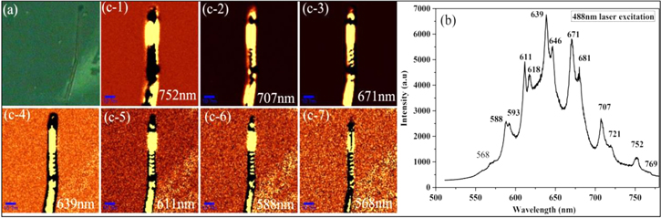
Figure 6. (a) Bright-field optical image of a single Te–CdS nanowire. (b) PL spectrum. (c1–c7) Corresponding emission mapping images of all bands.
Download figure:
Standard image High-resolution imageThe effect of dopant concentration on PL is important. We integrated different Te concentrations on a single CdS nanowire and explored their emission properties. Figure 7(a) is an optical microscopy image, from which we can see different colors at two opposite ends. Figure 7(b) is an SEM image and figures 7(c)–(e) are the corresponding line scanning EDSs of the elements S, Cd, Te. The distribution of Cd was uniform along the longitudinal direction of the nanowire. However, the concentration of S at the left end was lower slightly than that at the right end. On the contrary, the concentration of Te was higher at the left end. Therefore, this nanowire had asymmetrical Te dopant distribution, in which heavy Te-doping caused a dark color while low doping produced a light color (figure 7(a)). We then investigated the PL at the two opposite ends (figure 7(f)). At the right end, multi-mode emission was observed, similar to figure 3. However, only one broad PL band was obtained at the left end. Moreover, this broad band showed a red shift and weak PL intensity compared to the multi-mode emission. Therefore, the doping concentration is an important parameter for modulating multi-mode emissions. The heavy Te-doping produced more defect density, leading to the destruction of the transportation path along the WGM cavity. The absence of a resonating strength resulted in weak PL intensity. More Te doping can also form more CdTe, a poor emission material due to its dark exciton nature [46].

Figure 7. (a) Optical microscopy image of a single Te–CdS nanowire with different dopant concentration integration at the two opposite ends. (b)–(e) SEM and corresponding EDS line scanning of S, Cd, Te. (f) PL spectra at the left (with 0.01 standard excitation power) and right end (with 0.1 standard excitation power).
Download figure:
Standard image High-resolution imageDue to the bandgap (2.45 eV) or exciton absorption, pure CdS can only be excited with a light wavelength less than 500 nm. The emission center at 680 nm of the Te–CdS nanowires in this paper may indicate that they can be excited with a light wavelength larger than 500 nm. Figure 8 shows the PL spectra by using violet 355 nm, green 532 nm and red 632.8 nm lasers as the excitation light source. The three PL spectra show almost the same spectral profile, indicating that these multi-mode emissions were not the energy transfer from the bandgap or exciton to the trap bands. So, in comparison with pure CdS, the Te–CdS showed an extended absorption band in the red range (632.8 nm) or even the infrared range (875 nm) according to the PL results and may act as new solar cell absorbers and a broad spectral response photodetector material [47].

Figure 8. PL of a single Te–CdS nanowire under different laser excitation wavelengths.
Download figure:
Standard image High-resolution image
Conclusions
In summary, high-quality hexagonal Te-doped CdS nanowires were synthesized via a two-step CVD method with a magnetic force assistant substitution source material. Micro-Raman spectra of individual Te–CdS nanowires demonstrated the occurrence of evident SO phonon and strong electron–phonon interaction profiles, which play an important role in the luminescence tailor. In situ μ-PL characterization exhibited dominant broad defect state emission extension to far below its bandgap and could still be confined to propagate within the surface boundary and resonate to produce a broad multi-mode WGM emission from 560 nm to 870 nm. Contradictory to the classic WGM resonator, the present cavity emission peak position had continuous shifts under increasing excitation power and decreasing temperature. Moreover, the lifetime decay of all the emission peaks depended on their wavelength at room temperature. This difference reduced at lower temperatures. All of these novel results demonstrate the strong confined carrier interaction via surface phonon/polaron coupling within an active micro-cavity. The nonlinear emission process of Te–CdS might find important applications in solar cell absorbers, broad spectral response photodetectors, slow light devices, evanescent-wave sensors and topological insulator lasers.
Acknowledgments
This work was supported by the National Natural Science Foundation of China (Grant Nos. 11574081, 21661010, 21461006, 51472053) and the Scientific Research Fund of Hunan Provincial Education Department (Grant No. 14A096).