
Abstract
A simple methodology to prepare sub-100 nm resist nanopatterns with a high aspect ratio for the transfer of device nanofeatures is demonstrated. The novel method is based on a two- or multi-step developing process with the incorporation of an ∼4 nm thick metal film to protect the fine resist nanopatterns in the developer solution. Using this approach, sub-100 nm resist nanopatterns of different shapes were readily fabricated using the positive- and negative-tone electron-beam resists. Subsequently, fine device nanostructures could be readily converted from these fine resist nanopatterns with a high aspect ratio.
Export citation and abstract BibTeX RIS
1. Introduction
Metallic nanostructures in the sub-100 nm scale have been drawing more attention due to their many fascinating uses in functional nanodevices, such as high density magnetic patterned media, integrated circuit (IC) chips and high density magnetic write/read heads [1–4]. A widely used simple method to fabricate these nanostructures is through the conversion of fine resist nanopatterns via dry etching [5–7]. When using the dry-etch method, in particular ion-beam etching, to carry out the pattern transfer, a high aspect ratio (height to width ratio more than 1) for the fine resist nanopatterns is required as they usually possess similar or lower etch rates to that of the metallic materials [8]. However, it is difficult to achieve a high aspect ratio for resist patterns in the sub-100 nm scale, in particular a size finer than 50 nm, with the use of current commercial electron beam (e-beam) resists [9, 10]. This is attributed to the limited strength, etch resistance or large surface tension of the fine resist nanopatterns in developer solutions [11]. Although it has been reported that fine resist nanopatterns with a high aspect ratio could be achieved with methods such as mixing/doping of carbon nanotubes [12] or metal nanoparticles [11] into resists and using CO2 gas to dry the developed resists [13], these methods either require a complex resist mixing/doping process [11, 12] or are limited to special resists exhibiting high strength, such as hydrogen silsesquioxane (H8Si8O12, HSQ) [13]. Thus, the search for a viable method, which can utilize commonly used commercial resists for the high aspect ratio resist nanopatterns in the sub-100 nm scale, is interesting and highly sought after for current and future fine nanodevice fabrication in nanotechnology, semiconductor, data storage and microelectronics industries. In this work, we demonstrate a general simple approach to the fabrication of sub-100 nm high aspect ratio resist nanopatterns with a two-step developing method. This method presents a feasible means for almost all common commercially used positive and negative resists in the preparation of fine (sub-100 nm in size) and ultra-high-density (sub-100 nm in pitch size) resist nanopatterns.
2. Experimental details
An approximately 100 nm thick resist was first coated on the thin device film/wafer substrate and exposed using a high resolution (≤2 nm) e-beam nanolithography system (ELS-7000). The resist on the wafer was then partially developed by emerging it in the developer for half of the usual developing time. Subsequently, a thin metal film of approximately ∼4 nm in thickness was deposited on the resist nanopatterns at room temperature via low-energy sputtering or evaporation using an e-beam evaporator. During the deposition, the sample surface was normal to the metal-target source. Then, the resist patterns were further fully developed in the developer for the remaining half of the developing time. The fine resist nanopatterns with a high aspect ratio were achieved using the above-mentioned method. The device nanostructures of the required thickness were then converted from the resist nanopatterns via dry-etching and lift-off procedures. In the nanolithography process, negative-tone ma-N 2401 or HSQ e-beam resist and positive-tone ZEP(520A) or polymethyl methacrylate (PMMA) resist were used. The developers used were maD 525, 25% (w/w), tetramethyl ammonium hydroxide (TMAH), ZED-N50 (with ZMD as the rinsing solution) and a mixed solution (1 MIBK(methyl isobutyl ketone) : 3 IPA (isopropyl alcohol) for maN 2401, HSQ, ZEP and PMMA resists, respectively. The total developing time fell between 30 and 45 s. During the transfer of resist to the device nanopatterns, a Microetch ion beam system (IBE, RF-350) was used for the dry etch. Resist lift-off was carried out by immersing the sample in Remover PG solution or acetone solvent in an ultrasonic bath for 20–30 min. The thickness and images of all nanopatterns were measured using an atomic force microscope (AFM, Dimension 3100) or a field emission scanning electron microscope (FESEM, JSM 7401F). The measurement methods and resist exposure energies were similar to those reported previously [11].
3. Results and discussion
High aspect ratio resist nanopatterns in the sub-100 nm scale were prepared using commercial positive- or negative-tone resists via a two-step developing method. Figure 1 shows the preparation scheme. The successful fabrication of the fine resist nanopatterns was achieved by coating an ∼4 nm thick metal film on top of the resist nanopatterns after half of the usual developing time to preserve the high aspect ratio.
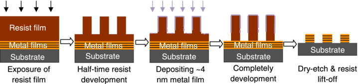
Figure 1. Schematic illustration of the preparation method for high aspect ratio resist patterns in the sub-100 nm scale based on a two-step development method as well as the subsequent conversion into device nanopatterns.
Download figure:
Standard imageWith the use of a conventional one-time developing method to prepare fine and high aspect ratio resist nanopatterns, faulty nanopatterns were usually produced. The nanopatterns were either over-developed or non-uniform in height. Figures 2(a) and (b) show the AFM profile of such defective sub-100 nm resist nanopatterns, prepared via the conventional developing method with ∼100 nm negative maN 2401 and positive ZEP resists, respectively. From the profile images, it is evident that the conventional method produced poor resist nanopatterns with a low aspect ratio. With the implementation of the two-step developing method depicted in figure 1, relatively uniform sub-100 nm resist nanopatterns (shown in figures 3(a) and (b)) of similar size and pattern density as above were achieved using the same maN 2401 and ZEP e-beam resists. The bottom image of figure 3(a) depicts that the height of the resist nanopatterns obtained after the second developing cycle (∼25 s) was much higher than that after the first developing cycle (∼15 s, figure 3(a) top image). In addition, the flattened metal surface between the nanofeatures at the bottom of the resist nanopatterns (bottom image of figure 3(a)) indicates a complete development of the resist to the bottom metal film. Thus, it was evident that the two-step developing method was capable of producing nanostructures of a high aspect ratio greater than 2:1.

Figure 2. (a) Poor sub-100 nm nanopillar structures prepared via the conventional method using ∼100 nm ma-N 2401 negative resist. (b) Poor sub-100 nm nanoarray structures prepared via the conventional method using ∼100 nm ZEP positive resist.
Download figure:
Standard image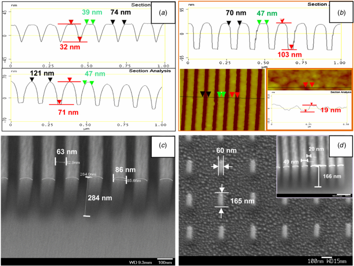
Figure 3. (a) Sub-100 nm nanopillar structures prepared via the proposed two-step developing method using ma-N 2401 negative resist. The top and bottom diagrams show the AFM measurements of resist nanopatterns developed with 15 (half-developing time) and 25 s, respectively. (b) Sub-100 nm nanoarray structures prepared via the two-step developing method with a developing time of 2 × 20 s using ZEP positive resist. The bottom-right inset of (b) shows the rough ma-N 2401 resist surface after undergoing partial developing. (c) and (d) FESEM images of sub-100 nm high aspect ratio 3D resist nanoarrays and nanopillars prepared via the three-step developing method with (c) PMMA and (d) HSQ resists.
Download figure:
Standard imageThe enhancement in the aspect ratio of the fine resist nanopatterns prepared via the two-step developing method was attributed to the presence of the ∼4 nm thick metal film, which was deposited after the partial development of the exposed resist. As illustrated in figure 1, the thin metal film wrapped the top portions of the partially developed resist nanopatterns after the first development cycle. This improved the strength of the resist nanopatterns, etch resistance to the developer as well as reduced the resists' surface tension in the developer solution. It is because as compared to the resists (with or without e-beam exposing), the thin metal film had a lower surface tension in the developers [11] and could also withstand a longer exposure time to the developer. As a result, the collapse of the nanopatterns, leading to non-uniform structures, could be prevented or largely alleviated. In addition, it should be noted that the profile of the fine resist nanopatterns was not affected during the deposition of the ∼4 metal film, as the deposition took place at low energy and room temperature via sputter and e-beam evaporator systems. It is also noteworthy that in the subsequent developing step, the deposition of the thin metal film did not affect the exposure of the bottom portions of the partially developed resist nanopatterns to the developer solution. This is attributed to the fact that the top portions of the partially developed resist nanopatterns, possessing relatively smooth surfaces from the high resolution (∼2 nm) e-beam exposure, were almost fully encapsulated by the ∼4 nm metal film, but the bottom portions of the partially developed resist nanopatterns were not. The non-fully encapsulated bottom portions were the result of the rough resist surface at the bottom trenches, which were formed when the resist was partially developed away through the first development cycle (figure 1). The surface in the trench regions typically possessed an average roughness (Ra) larger than 10 nm for common e-beam resists, which was much larger than the thickness of the thin metal film deposited. The inset of figure 3(b) shows the rough surface step of the ma-N 2401 resist at the bottom trench to be nearly 20 nm after the partial development. Furthermore, at a vertical deposition angle, the thickness of the deposited thin metal film at the trenches of resist patterns was also thinner than that deposited on the resist top portions due to the shading and adsorbing effect of the top partials of resist nanopatterns, particularly for high-density nanopatterns. Thus, the ∼4 nm thin metal film deposited only wrapped the top portions of the nanopatterns without covering the whole rough resist surface at the bottom of the nanopatterns (especially at the trench angles). As such, the developer solution could readily penetrate into the bottom resist portions for the further development and the deposited thin metal films would not prevent the bottom resists from undergoing further development in the subsequent step. However, for the resists (e.g., maN 2401) with a relatively low resolution and etch resistance to the developer, more investigation revealed that even with the ∼4 nm thin metal film coated onto the resist nanopatterns after the first development cycle, too long a time for the second development cycle (such as ≥ 25 s for maN 2401) could lead to resist nanopatterns with an irregularly shaped (unflattened) top surface (shown in the bottom image of figure 3(a)). A thicker metal film (e.g. 8 nm) might be deposited to alleviate the issue of irregular fine nanopattern shape. However, too thick a metal film would result in the difficulty in further development.
To further ascertain the effectiveness and consistency of the two-step developing method, the process was extended to other e-beam resists such as PMMA positive-resist and HSQ negative-resist for the fabrication of high aspect ratio resist nanopatterns. Figures 3(c) and (d) show that uniform resist nanopatterns with a high aspect ratio were also similarly produced. In addition, our further investigation results also revealed that for resist thickness greater than 120 nm, the developing process could be divided into more cycles/steps while keeping the overall developing time constant or slightly longer. Figure 3(c) and the inset of figure 3(d) indicate the resist nanopatterns obtained from a three-step developing process, which involved the deposition of the thin metal film twice. Notably in the figures, to enhance the contrast of the nanoarrays in the top-views of FESEM images, according to the stripe and color differences between the tops and sidewalls of the resist nanopatterns, the joint-lines were identified and marked between the pattern tops and sidewalls. This multi-developing method could also be extended to the preparation of bigger nanopatterns, more than 100 nm in scale, with a high aspect ratio in the event that the resists possessed low resolution and poor developer-etching resistance.
The fabricated resist nanopatterns with a high aspect ratio could be readily converted to high-quality device nanopatterns. Figures 4(a) and (b) show smooth and uniform device nanopatterns in the sub-100 nm scale prepared from these resist nanopatterns. The thin ∼4 nm metal film was further shown to not only serve as a protection toward the high aspect ratio resist nanopatterns during the developing process, but also during the dry-etching process of device pattern transfer. The thin metal film was able to transfer the high ion-energy away quickly during dry etching, thus preventing the burning or ageing of the fine resist nanopatterns under the high ion-beam energy. Moreover, the thin metal film improved the dry-etching resistance of the fine resist nanopatterns. As a result, the thin metal film minimized the difficulty in lifting-off resist residues in the remover solvent or solution after the dry etch. Figure 4(c) depicts the successful fabrication of the uniform trilayer metal–sensor–metal memory devices, with GMR nanosensors of ∼80 nm at each crosspoint, using the two-step developing method.

Figure 4. (a) and (b) FESEM images of converted high-density sub-100 nm 3D multilayer CoPt (a) arrays and (b) pillars from the high aspect ratio resist nanopatterns. The inset of (a) shows the AFM cross-sectional analysis of the nanoarrays. (c) AFM image of the converted memory device containing ∼80 nm metallic sensors at each cross-point.
Download figure:
Standard image4. Conclusion
A general, simple process for the preparation of sub-100 nm resist patterns with a high aspect ratio has been demonstrated. By means of a two-step developing process which combined the utilization of a ∼4 nm thick metal film, the prepared high aspect ratio resist nanopatterns could be readily converted to smooth and uniform device nanopatterns in the sub-100 nm scale. This method has proven to be suitable for almost all positive- and negative-tone e-beam resists. The methodology provides an easy solution for the industries to carry out the fabrication of fine sub-100 nm nanodevices using commercial e-beam resists.