
Abstract
We propose a gimbal-less two-axis electrostatic microelectromechanical system (MEMS) scanner with tilted stationary vertical combs (TSVCs) fabricated via a microassembly process. The gimbal-less two-axis scanner has the advantage of being of a compact size and also does not need any additional fabrication sequence for electrical isolation. The TSVCs and coupled springs (T-shaped springs and folded springs) allow the mirror scanner to rotate around two axes with a large scanning angle. The fabrication steps for the proposed scanner can be remarkably reduced by employing a microassembly process, as there is no need to conduct a multistep etching process for height offset between two vertical combs. It was found that the width of the folded spring and the T-shaped spring dominated the resonant frequency of the fast axis and the slow axis, respectively. By modeling the capacitance change of TSVCs with respect to the rotational angle (θ), the effective tilted angle (ETA), as a new design criterion, was introduced to determine an adequate operation range. The optical scanning angle of the fabricated scanner was up to 7.8° at 90 V for the slow axis in quasistatic mode and up to 17.3° at 100 V for the fast axis in resonant mode at 2.84 kHz. The fabricated scanner can be used for various endoscopic optical applications.
Export citation and abstract BibTeX RIS
1. Introduction
MEMS scanners have been widely used in various optical applications owing to their compact size, increased speed, batch fabrication, cost effectiveness, low power consumption, etc. [1]. The one-axis scanner has evolved into the two-axis scanner to meet the requirements of optical systems such as projection displays [2–4], optical communications [5], laser ablation systems [6], and biomedical imaging [7–10]. Among the actuation methods of MEMS scanners, electrostatic actuation is attractive as it enables a compact size, low power consumption and simple fabrication. In electrostatic actuation, angular vertical combs (AVCs) are known to have a larger scan angle than that of conventional staggered vertical combs (SVCs [11]).
Quasi-static two-axis scanners with vertical offset of the comb electrodes have been investigated by many research groups; a gimbaled AVC mirror was fabricated using surface-micromachined latches and a bulk micromachining process [12]; a gimbaled monolithic mirror with AVC was fabricated by plastic deformation of torsional springs [13]; a gimbaled mirror scanner with a self-aligned SVC was made by complicated multi-etching and wafer bonding [14, 15]; a gimbal-less monolithic tip-tilt-piston SVC micromirror was realized using a multi-etching process of deep reactive ion etching (DRIE [16]); and two one-axis AVC mirrors fabricated by photoresist (PR) reflow were monolithically cascaded to realize a two-axis scanner [17]. However, the previous fabrication methods of comb electrodes with vertical offset (AVC or SVC) are complicated due to multi-etching or precise alignment. Recently, a microassembly process was developed to alleviate the difficulty in the fabrication of comb electrodes with vertical offset [18, 19]. The microassembly process can also easily provide a gimbal-less scanner with electrical isolation between two axes, whereas the gimbaled scanner requires an additional process of electrical isolation between the inner frame (fast axis) and outer frame (slow axis), which are mechanically connected.
In this paper, we propose a gimbal-less two-axis electrostatic MEMS scanner with tilted stationary vertical combs (TSVCs) fabricated via a microassembly process. Our previous work proposed an one-axis scanner with movable AVCs [18]; however, the device proposed in this paper is a gimbal-less two-axis scanner with TSVCs and coupled springs. The TSVCs enable the gimbal-less optical scanner to operate even in two axes with a stable angular motion, which is not the case for the previous one-axis scanner with movable AVCs [18]. The microassembly process can significantly reduce the complexity of scanner fabrication, as there is no need to add an insulation layer or to conduct a multistep etching process. The proposed scanner is also of a compact size, which will be justified in section 2. The tilted angle (vertical offset) of the comb electrodes can be easily controlled by using the proposed microassembly process, which contrasts with the case of other fabrication methods [20]. The maximum rotational angle of the mirror is determined by the effective tilted angle (ETA), which can be theoretically derived from the geometric model of comb electrodes. A parametric study of the employed springs was also conducted using the finite element method (FEM); the fabricated scanner was evaluated in terms of scanning angle and resonant frequency.
2. Configuration and principle
Figure 1 shows a schematic of the gimbal-less two-axis electrostatic scanner with TSVCs that is fabricated via a microassembly process. The scanner consists of a device section based on a silicon-on-insulator (SOI) wafer and a tilting section made of polymer (SU-8). The device section comprises six components: T-shaped springs, folded springs, tilting levers, comb actuators, a mirror, and alignment holes. The tilting section comprises tilting pillars and alignment pillars. In the microassembly process, the tilting pillars push down the tilting levers when the tilting section is put on the device section. Consequently, TSVCs are produced as the stationary comb electrodes are tilted in a manner approximating a seesaw, as shown in figure 2.
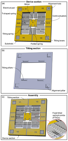
Figure 1. Schematic of the gimbal-less two-axis electrostatic scanner with TSVCs: (a) device section, (b) tilting section (upside down image), and (c) microassembly after tilting section is put down on the device section.
Download figure:
Standard image High-resolution image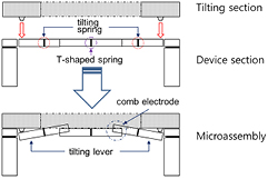
Figure 2. Schematic of TSVCs realized by a microassembly process. (a1) Applying input voltage for the slow-axis scanning. (a2) The slow-axis scanning in the quasistatic mode of the scanner with TSVCs. (b1) Applying input voltage for the fast-axis scanning. (b2) The fast-axis scanning in the resonant mode of the scanner.
Download figure:
Standard image High-resolution imageDuring microassembly, the stationary comb electrodes connected with tilting levers are tilted at a certain angle, whereas the movable comb electrodes lie in a horizontal position as fabricated. Then, the tilting section is bonded to the surface of the device section, fixing the tilting levers and stationary comb electrodes at the determined angle. The micromirror of the scanner can be rotated bidirectionally because stationary comb electrodes, placed on opposite sides of the movable comb electrodes connected with the micromirror, are tilted above the movable comb electrodes, as shown in figure 2. The tilted angle of the stationary comb electrodes (α) can be adjusted according to the equation, α = h/la, where h is the height of the tilting pillar and la is the arm length (distance between the rotational axis of the tilting lever and the tilting pillar).
Two-axis scanning is performed by simultaneous operation of the quasistatic mode for the slow axis and the resonant mode for the fast axis. To bidirectionally drive the mirror around the slow axis in quasistatic mode, electric voltages V1 and V3, with the same amplitudes but out of phase to each other with the DC bias voltages, are applied to the scanner, as shown in figure 3(a1). The slow-axis scanning is achieved by balancing between the applied electrostatic force and the restoring force of the T-shaped springs as shown in figure 3(a2).
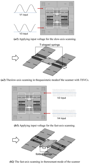
Figure 3. Operation principle for two-axis scanning of the gimbal-less two-axis electrostatic scanner with TSVCs; (a1) applying input voltage with V1 and V3 of the identical amplitude but 180° phase difference, (a2) the slow-axis scanning shape when the input voltage is applied quasistatically, (b1) applying input voltage with V2 and V4 of the identical amplitude and phase, and (b2) the fast-axis scanning shape when the input frequency is equal to the resonant frequency of the fast axis.
Download figure:
Standard image High-resolution imageTo actuate the mirror around the fast axis in the resonant mode, V2 and V4 with identical amplitude and phase are applied to the scanner, as shown in figure 3(b1). The frequency of the applied voltage should be the same as the resonant frequency of the seesaw mode, which is achieved by bending the T-shaped springs and twisting the folded springs as shown in figure 3(b2).
The compliant springs employed for the two-axis scanning were the T-shaped springs and the folded springs. The shapes and dimensions of each spring are displayed in table 1. Through FEM simulation, the T-shaped spring and the folded spring were found to be related to the resonant modes of the slow axis and the fast axis, respectively. When the width of the folded spring was increased from 3 μm to 20 μm, the resonant frequency of the fast axis increased by five times; whereas the resonant frequency of the slow axis decreased by only 1.3%, as shown in figure 4. Meanwhile, when the width of the T-shaped spring was extended from 3 μm to 20 μm, the resonant frequencies of the slow axis went up by ten times, while the fast axis case increased merely by 14%.
Table 1. Spring dimensions for two-axis gimbal-less scanner.

Figure 4. Resonant frequency with respect to the width of (a) folded spring, and (b) T-shaped spring.
Download figure:
Standard image High-resolution imageThe proposed gimbal-less two-axis electrostatic scanner, which is implemented with TSVCs and serially connected springs, is of a compact size compared with other types, including: the gimbal-less cruciform type, such as the gimbal-less monolithic micromirror [16]; the gimbal type, such as the gimbal-suspended AVC mirror [12, 13]; and the cascade type, such as cascaded micromirror pairs [17]. Given conditions in which the number of combs, the mirror size, the electric pad size, and the spring length are identical, the proposed scanner was estimated to occupy the smallest area. From the related calculations, the gimbal-less cruciform type is 91% larger, and the gimbal type is 10% larger than the proposed gimbal-less type.
3. Analysis
3.1. Analysis of comb electrode
As opposed to previous scanners with movable AVC electrodes, the stationary combs of the scanner in this paper are tilted instead of movable combs, as can be seen in figure 5. TSVCs are favorable to realize two-axis scanning with compact size and stable operation for a gimbal-less scanner.

Figure 5. Schematic and geometries of TSVCs.
Download figure:
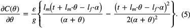
Standard image High-resolution imageFigure 5 also shows the structure and dimensions of the comb electrode, where t is the thickness of the comb fingers, lf is the length between the tilting spring and the end of the movable comb finger, θ is the rotational angle of the movable comb finger, and α is the tilted angle of the stationary comb fingers, which does not exceed the angle of arctan (t/lf). The mechanical rotational angle (θ) moves from zero to the maximum angle, which corresponds to the maximum capacitance formed between the two comb electrodes. Thus, the capacitance equation varies depending on the ranges of the tilted angle (α), as shown in figure 6. For a static analysis for the slow axis, the equation for the electrostatic torque (Te) of the scanner with TSVCs can be obtained by taking the derivative of the capacitance, as in equation (1).
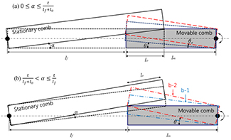
Figure 6. Rotational angle (θ) of the movable comb with respect to tilted angle (α) of the stationary comb: (a) tilted angle range from 0 to t/(lf + lo), and (b) tilted angle range from to t/(lf + lo) to t/lf. (b-1 represents the case that the top of the movable comb meets the bottom end of the stationary comb, and b-2 represents the case that bottom end of the movable comb meets the bottom of the stationary comb.)
Download figure:
Standard image High-resolution imageThe fringe fields were not taken into account in the following capacitance equations and capacitance derivatives, which might lead to inaccurate results, particularly in the case of thin comb electrodes or vertical offset beyond the overlap between two combs [11].
3.1.1. Tilted range of 0 ≤ α ≤  .
.

The capacitance and its derivative are expressed in equations (2) and (3), respectively, for the rotational range up to the effective rotational angle (θe = lf·α/lm), which corresponds to a certain angle when the distal bottom edge of the movable comb electrode meets the bottom of the stationary comb electrode, as indicated in figure 6(a).
For 
where ε is the permittivity of air, g is the lateral space (gap) between the comb electrodes, lo is the overlapped length between the stationary and the movable comb fingers, lm is the length of the movable comb fingers, and A1 is a constant related to the other comb dimensions and is irrelevant to rotational angle (θ). The equation for the rotational angle (θ) beyond the effective rotational angle (θe) was derived, but is not shown here because the rotational angle does not effectively increase with input voltage, which implies that the rotational angle in this range might not be adequate for scanning.
3.1.2. Tilted range of .

The capacitance equation and its derivatives are stated according the rotational angle ranges, b-1 and b-2, as shown in figure 6(b). A2 and A3 are also constants; those are irrelevant to the rotational angle (θ).


The equation for the rotational angle (θ) beyond the effective rotational angle (θe) was also derived, but is not shown here for the same reason as that in section 3.1.1.
Figure 7 expresses the capacitance change with respect to the rotational angle of the movable combs for a given tilted angle. The capacitance change becomes smaller for early rotational angles when the tilted angle (α) is larger than the critical tilted angle (3.6° in our design), which is equal to t/(lf + lo). The small capacitance change causes a small rotational angle for identical input voltage. Note that the capacitance change remains almost constant for a rotational angle up to the effective rotational angle (θe), depicted as circle (o) in figure 7, when the tilted angle is smaller than the critical tilted angle (3.6°). The capacitance change abruptly decreases when the rotational angle passes through the effective rotational angle (θe), resultantly requiring a large input voltage, as described in section 3.1.1. To obtain a larger rotational angle exceeding the effective rotational angle, input voltage is sharply increased with respect to the rotational angle (beyond effective rotational angle, θe) because the capacitance change is abruptly dropped as it passes through the effective rotational angle (θe). For an effective actuation of this scanner with the given geometries, the optimal tilted angle is theoretically 3.6° as shown in figure 7. However, the tilted angle is designed at 3.1° considering the fabrication error of 0.36° (10%) and the marginal error of 0.14°. Note that the maximum error of the fabricated tilted angle is 10% in the previous experiments [18].
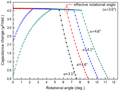
Figure 7. Capacitance change with respect to rotational angle of the movable comb electrodes. In our design, the critical tilted angle, t/(lf + lo), is 3.6°. If the tilted angle is larger than 3.6°, the capacitance change gets smaller for early rotational angle of the movable comb electrodes. Circle (o) represents the effective rotational angle for the given tilted angle (3.6°).
Download figure:
Standard image High-resolution image3.2. New design criteria for tilted angle
Figure 8 shows the rotational angles (θ) of the movable comb electrodes (or a mirror) that were theoretically calculated with respect to the tilted angle and the input voltage. When the magnitude of the applied voltage is given, the rotational angle initially increases with the increasing tilted angle, and saturates from α1 (the minimum of the required tilted angle). Here, the effective tilted angle (ETA) can be newly defined as the angle that allows the rotational angle to reach its maximum value. The ETA generally has an angle range between α1 and α2 (the maximum of the required tilted angle). For instance, the ETA ranges from 1.27° to 4.06° when the magnitude of the applied voltage is 100 V, as shown in figure 8.
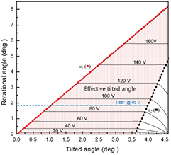
Figure 8. Rotational angle of the movable comb electrodes for the slow axis with respect to tilted angle when input voltage is applied. Effective tilted angle (ETA), where rotational angle keeps constant, includes the ranges between α1 (●) and α2 (■) for the given input voltage.
Download figure:
Standard image High-resolution imageIf the required rotational angle is given, α1 can be found using equation (8), which was derived using geometrical modeling. If the input voltage applied to the device is known, α1 is obtainable using equation (9), which can be derived from the equilibrium equation of the electrostatic torque (Te) and the mechanical torque (Tm) assuming that the capacitance derivative is constant between α1 and α2.


where Kθ is the stiffness of the torsional spring, V is the applied input voltage and θ is the input rotational angle at the given value.
The required maximum tilted angle (α2) is also obtainable using equation (10) for the given rotational angle (θ), and equation (11) for the given applied voltage (V).


The tilted angle of the scanner is determined considering the equation for ETA described above. However, fringe fields were not considered in the equations and might influence the behavior, particularly in the case of thin comb electrodes or considerable vertical offset [11]. We believe that the newly introduced design criteria as a first estimation for the tilted angle will be useful for the designers of TSVC scanners.
4. Fabrication
The device section was fabricated on an SOI wafer comprising a device layer (Si), a buried oxide (BOX), and a handle layer (Si) with thicknesses of 50 μm, 2 μm, and 400 μm, respectively. The tilting section was made from SU-8 (negative photoresist) that was sufficiently rigid for use in a mechanical structure after a lithography process. The fabrication sequence for each section and the microassembly processes are illustrated in figure 9.
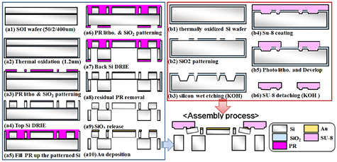
Figure 9. Fabrication sequence of the gimbal-less two-axis electrostatic scanner with TSVCs; (a) device section, (b) tilting section, and (c) microassembly process.
Download figure:
Standard image High-resolution imageIn the fabrication of the device section, the SOI wafer was thermally oxidized in a furnace to prepare the etch mask layer (1.2 μm in thickness) for the DRIE of the device pattern. The thermal oxide on the front side was patterned by reactive ion etching (RIE) using a PR mask formed by photolithography. The device patterns of the thermal-oxide etch mask were transferred to a 50 μm-thick device layer of the SOI wafer via the DRIE process until the etch-stop (BOX layer) was exposed. To protect the fabricated device layer while the wafer was upside-down during backside patterning, the front of the Si pattern was filled with PR. For the backside opening, the etch masks of the thermal oxide and PR were patterned by RIE and photolithography, respectively. To protect the fabricated device layer while the wafer was upside down during backside patterning, the front of the Si pattern was filled with PR. For the backside opening, the etch masks of the thermal oxide and PR were patterned by RIE and photolithography, respectively. The 400 μm thick handle layer was thoroughly etched via the DRIE process to provide an opening space for mirror rotation. Then, the PR residue was removed using an acetone solution, and each scanner chip in the wafer was separated by breaking the BOX layer between chips using tweezers. The release of the separated devices was conducted by etching out of the BOX layer between the device layer and the handle layer. As a final fabrication step of the device section, the mirror surface was sputtered with Cr and Au to obtain high optical reflectivity.
In the fabrication of the tilting section, a (100) silicon wafer was thermally oxidized to prepare an etch mask layer (1.0 μm in thickness) for anisotropic Si etching. The thermal oxide was patterned using photolithography and buffered oxide etching (BOE) solution. (100) silicon was then anisotropically wet-etched for 40 min using a potassium hydroxide (KOH) solution at a concentration of 34.5% and a temperature of 80 °C. The etched depth of the silicon was 30 µm, which corresponded to the height of the pillar. SU-8 (negative PR) with 500 µm in thickness, which is sufficiently rigid and thus suitable for the tilting section, was spin-coated onto the silicon wafer with etched cavities. As a final fabrication step of the tiling section, the frame of the tilting section was fabricated using a photolithography process; the frame was then detached from the silicon wafer.
In the microassembly process, four alignment pillars of the tilting section were stamped on the SU-8 layer (as gluing material) to be bonded in each alignment hole of the device section after curing. When the tilting section was assembled with the device section, the tilting pillars pushed down the tilting levers; the stationary electrodes were tilted as the last step of the scanner fabrication. To analyze the deformation of the tilting levers during the microassembly process, FEM simulation was conducted. ANSYS (FEM) simulation reveals that the deflection of the tilting spring is as small as 0.18 μm when the tilting levers connected to the tilting springs (width 10 μm, length 400 μm) were pressed downward by the tilting pillars. The deformation of the SU-8 tilting pillars (Young's modulus 2.0 GPa) is also negligible because the deformation of the tilting pillars is less than 2 nm in height when 1 mN (about ten times the actual required force) is applied.
The scanning electron microscope (SEM) images in figure 10 show the procedure of the microassembly for fabricating the gimbal-less two-axis electrostatic scanner: (a) the device section including a mirror (size 1 mm × 1 mm), T-shaped springs, folded springs, comb electrodes, tilting springs, alignment holes, and tilting levers; (b) the tilting section comprised of the tilting pillars and alignment pillars; and (c) a perspective view of the scanner after the microassembly.

Figure 10. SEM images of the fabricated two-axis scanner: (a) device section, (b) tilting section, and (c) two-axis scanner after microassembly process.
Download figure:
Standard image High-resolution imageFigure 11 shows the detailed view of the TSVCs before and after microassembly. The fabricated stationary combs keep the same level with the movable comb before two sections were assembled, as shown in figure 11(a). However, the stationary combs became tilted above the movable combs after microassembly, as shown in figure 11(b). The average tilted angle (α) for the fabricated scanners (five samples) was measured using a confocal microscope (NanoFocus) and found to be 3.1°. The maximum variance of this value was reduced from 10% (in the previous experiment) to 3% (in this study), which was achieved by careful adjustment between the alignment pillars and alignment holes.
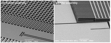
Figure 11. SEM images of the fabricated comb electrodes: (a) even comb electrodes before microassembly and (b) TSVCs after microassembly.
Download figure:
Standard image High-resolution image5. Experimental results
In order to find the resonant frequency of the fabricated scanner, the amplitudes of the mirror rotation were measured for the slow axis and the fast axis using a laser Doppler vibrometer (NeoArk MLD-211D). The amplitude of the input sinusoidal signal was held constant at 11 Vp-p (DC offset of 5.5 Vvias) while the driving frequency was gradually increased. The resonant frequencies of the fabricated scanner were experimentally found to be 1.65 kHz for the slow axis (rotation mode) and 2.84 kHz for the fast axis (seesaw mode), as shown in figure 12. Each resonant frequency is in good agreement with the designed one of 1.65 kHz for the slow axis and 2.74 kHz for the fast axis. To quantitatively evaluate the optical scanning angle, the experimental setup was prepared including a pigtailed laser diode (LD), a collimator, and a position sensitive detector (PSD, Hamamatsu C10443-03). For the slow axis (quasistatic actuation at 30 Hz), as can be seen in figure 13, the total range of the measured optical scanning angle was as large as 7.8° at 90 V. The measured optical scanning angle for the slow axis is well matched to the theoretical value within the maximum error of 7% (not shown). It should be noted that the slow axis is bidirectionally actuated by applying the input voltage of V1 (squares) or V3 (circles).
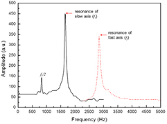
Figure 12. Rotational amplitude of the mirror with respect to the input frequency when the input voltage (Vac + Vbias) is applied; fs is resonance of the slow axis and fs/2 is imaginary resonance produced by bias voltage, and ff is resonance of the fast axis.
Download figure:
Standard image High-resolution image
Figure 13. Measured optical scanning angle of the fabricated two-axis scanner. The square (■) and the circle (●) represent bidirectional slow-axis scanning excited in a nonresonant/quasistatic mode, and the triangle (▲) indicates the fast-axis scanning excited in a resonant mode.
Download figure:
Standard image High-resolution imageThe tilted angle (α) of the fabricated scanner was measured and found to be 3.1°, which meets the requirement that the tilted angle should be smaller than the critical tilted angle (3.6° as described in section 3.1.2). Thus, optical scanning was confirmed to be effective in terms of rotation angle when the range of ETA is between α1 and α2. The overall optical scanning angle of the slow axis was measured to be 7.8° at 90 V, which can be equivalently converted into a rotation angle of ±1.95° (= half of optical scanning angle of ±3.9°). The theoretical rotation angle can be seen to be 1.85° in figure 8, which matches well with the experimental value.
Optical scanning for the fast axis (triangles) can be activated by applying the same input voltage both to V2 and V4 at the resonant frequency of 2.84 kHz. The optical scanning angle was 5.28° at 60 Vp-p and 17.3° at 100 Vp-p. Figure 14 shows the various operation frequencies of the slow axis when the fast axis is fixed at the resonant frequency of the seesaw mode. Figure 14(a) is a raster scanning image at 60 Hz actuation of the slow axis; figures 14(b)–(d) provide the Lissajous patterns for the various ratios of scanning frequency of the slow and fast axes. Thus, we can say that two-axis scanning of the fabricated gimbal-less electrostatic scanner has been successfully demonstrated, implying that the proposed optical scanner has high potential for various optical applications including endoscopic optical coherence tomography (OCT) and photoacoustic imaging.

Figure 14. The measured scanning pattern of the fabricated two-axis scanner: (a) raster scanning, Lissajous pattern of frequency ratio (b) 1:2, (c) 1:3, and (d) 3:4.
Download figure:
Standard image High-resolution image
6. Conclusions
A gimbal-less two-axis electrostatic scanner with TSVCs has been successfully implemented using a microassembly process. TSVCs allowed the mirror to rotate bidirectionally on the slow axis. Two-axis scanning was successfully demonstrated with the folded springs and the T-shaped springs by way of simultaneous operation for the slow axis and the fast axis. It was confirmed that the folded spring was dominant in the resonant frequency for the fast axis and the T-shaped spring was mainly related to the resonant frequency for the slow axis. The ETAs (α1 and α2) and the maximum rotational angle could be derived from the equations of the geometrically modeled capacitance between two comb electrodes. The effective tilted angle can be used as an important criterion in the design of an electrostatic actuator with TSVCs.
The efficacy of the microassembly, which does not require a complicated process, was validated by evaluating the variance of the tilted angle of the fabricated gimbal-less two-axis scanner. The measured optical scanning angles of the fabricated scanner were as large as 7.8° at 90 V for the slow axis (quasistatic mode) and 17.3° at 100 Vp-p for the fast axis (resonant mode). The fabricated scanner can be used for various optical applications such as endoscopic optical coherence tomography (OCT) and photoacoustic imaging systems.
Acknowledgements
This research was supported by a grant from the Institute of Medical System Engineering (iMSE) at GIST, Korea.