

Abstract
Micro-electromechanical system (MEMS) technologies were used to develop a thickness-mode piezoelectric micromachined ultrasonic transducer (Tm-pMUT) annular array utilizing a lead magnesium niobate–lead zirconate titanate (PMN–PZT) single crystal prepared by the solid-state single-crystal-growth method. Dicing is a conventional processing method for PMN–PZT single crystals, but MEMS technology can be adopted for the development of Tm-pMUT annular arrays and has various advantages, including fabrication reliability, repeatability, and a curved element shape. An inductively coupled plasma–reactive ion etching process was used to etch a brittle PMN–PZT single crystal selectively. Using this process, eight ring-shaped elements were realized in an area of 1 × 1 cm2. The resonance frequency and effective electromechanical coupling coefficient of the Tm-pMUT annular array were 2.66 (±0.04) MHz, 3.18 (±0.03) MHz, and 30.05%, respectively, in the air. The maximum positive acoustic pressure in water, measured at a distance of 7.27 mm, was 40 kPa from the Tm-pMUT annular array driven by a 10 Vpp sine wave at 2.66 MHz without beamforming. The proposed Tm-pMUT annular array using a PMN–PZT single crystal has the potential for various applications, such as a fingerprint sensor, and for ultrasonic cell stimulation and low-intensity tissue stimulation.
Export citation and abstract BibTeX RIS
1. Introduction
Ultrasonic transducers are devices that convert electrical energy to mechanical vibrations or vice versa. There are two types of ultrasonic transducer, the bulk ceramic transducer and the micromachined ultrasonic transducer (MUT), which uses micro-electromechanical system (MEMS) technology [1]. Bulk ceramic transducers are fabricated by dicing using piezoelectric ceramics to produce devices resonating in the thickness direction [2]. Due to the size of the diamond blades, the minimum gap between two adjacent elements is limited (generally > 50 µm) and the ceramic transducer is relatively large [3]. MUT is being developed as an alternative to traditional ultrasonic transducers because of its various advantages, including direct integration of electrical connections, precise fabrication, low driving power, and high sensitivity [4, 5]. Depending on the operating principle, there are two types of MUT: capacitive MUT (cMUT) [6, 7] and piezoelectric MUT (pMUT) [8, 9]. cMUT has potentially higher bandwidth and sensitivity, but the acoustic power is limited because the displacement of the diaphragm (the vibrating component) is limited to the gap between the top and bottom electrodes to prevent a pull-in effect [10, 11]. The cMUT also requires a high DC bias voltage for ideal bandwidth and sensitivity. The high DC bias may also cause safety issues in human applications. In contrast, pMUT has a higher displacement because it does not have a displacement limit or pull-in effect [12, 13].
Ultrasound transducers can be operated in thickness mode, which emits and receives sound waves along the direction of the thickness of the piezoelectric layer. A conventional piezoelectric ultrasound transducer operates in thickness mode, and the resonance frequency is determined by the thickness of the piezoelectric layer [14]. Also, the piezoelectric constant d33 is characterized by the piezoelectric thickness mode. For thickness-mode devices operating in the 1–10 MHz range, the thickness of the piezoelectric layer should be 100–1000 µm. For a bulk transducer, this thickness can be achieved by lapping bulk ceramic, but it is difficult or impossible to make the same thickness by the sol–gel method for pMUT fabrication [14]. Therefore, a bending mode is used to operate pMUTs in this frequency range. In a bending mode, the resonance frequency is controlled by the diameter and thickness of the diaphragm [15]. To increase the acoustic intensity of the pMUT in bending mode, a piezoelectric material with a high piezoelectric constant and a large membrane is required to achieve a large displacement. For this reason, the conventional bending mode pMUT has a limitation in achieving high acoustic intensity with high resonance frequency due to the limited diameter of the membrane, which limits membrane displacement. In this study, these limitations were overcome by fabricating a pMUT that operates in thickness vibration mode using thick lead magnesium niobate-lead zirconate titanate (Pb((Mg1/3, Nb2/3)x − ZrTi(1 − x))O3, PMN–PZT) single crystal and MEMS processing technology.
Lead zirconate titanate (PZT) deposited by the sol–gel method is a piezoelectric material widely used for pMUTs as its film grain size, composition and orientation are favorable for MEMS fabrication. PZT is physically strong, chemically stable, and inexpensive to deposit [16]. However, the dipole domains in the sol–gel PZT are randomly oriented, and it is not possible to align all dipoles in one direction, even after poling [17]. The achievable thickness of the sol–gel PZT is limited to a few micrometers. Lead zinc niobate-lead titanate (Pb(Zr1/3, Nb2/3)O3–PbTiO3, PZN-PT) and lead magnesium niobate-lead titanate (Pb(Mg1/3,Nb2/3)O3–PbTiO3, PMN-PT) have been developed to enhance the crystal orientation of piezoelectric single crystals [18, 19]. These single crystals have higher electromechanical (EM) coupling factors (Qm) and piezoelectric constants compared to PZT [20–25]. However, PZN-PT and PMN-PT piezoelectric single crystals have low phase-transition temperatures (TRT = 124 and 90 °C, respectively) [16, 26] between their rhombohedral and tetragonal phases and a low coercive electric field (EC = 2–3 kV cm−1) [27, 28]. The dielectric and piezoelectric properties of PZN-PT and PMN-PT piezoelectric single crystals will be significantly reduced if the working temperature is above the TRT, which is the upper limit of the allowable temperature range of these single crystals. Therefore, the working temperature for PZN-PT and PMN-PT piezoelectric single crystals must be controlled to maintain a high Qm and EC for use as an ultrasonic transducer. Those PZN-PT and PMN-PT piezoelectric single crystals with low TRT are known as first-generation piezoelectric single crystals, and the manufacturing costs are higher than that of the PZT.
Second-generation piezoelectric single crystals, including PMN–PZT, were introduced to increase the TRT by applying the solid-state single crystal growth (SSCG) method, which has various advantages, such as no melting process, mass production, and low production cost [20, 29–31]. Therefore, the PMN–PZT single crystal may improve the production cost and repeatability of MEMS devices, thereby enabling their mass production. However, use of PMN–PZT single crystals for MEMS fabrication is relatively new and few studies have assessed its patterning. In particular, a method for dry etching of PMN–PZT single crystals may be required for fabrication of next-generation piezoelectric MEMS devices with PMN–PZT. We report a fabrication method for PMN–PZT single crystals, regarding the etch rate, piezoelectric properties, and compatibility with other materials. Dry etching of PMN–PZT single crystals was performed by metal inductively coupled plasma-reactive ion etching (ICP-RIE), and their etching parameters were investigated using x-ray photoelectron spectroscopic (XPS) analysis and surface profiling. The developed fabrication process was used to fabricate a thickness-mode pMUT (Tm-pMUT) annular array using a PMN–PZT single crystal, and Tm-pMUT was characterized. The proposed Tm-pMUT annular array using PMN–PZT single crystals could be used for various applications, such as a fingerprint sensor, and for ultrasonic cell stimulation and low-intensity tissue stimulation.
2. Design and fabrication of a Tm-pMUT annular array
Table 1 shows the design parameters of the Tm-pMUT annular array based on a PMN–PZT single crystal. The Tm-pMUT annular array consists of eight rings. The width of each ring is 120 µm and the thickness of the PMN–PZT single crystal is 300 µm. The outer diameter of the annular array was designed to be 6520 µm, based on the flexural-mode pMUT annular array reported by our group [32]. Figure 1 shows optical images and a schematic of the fabricated Tm-pMUT annular array. The top electrodes and connection line for each ring element are indicated on top of the PMN–PZT single crystal. In general, the annular shape produces a geometrically narrow ultrasound beam profile, which enables the Tm-pMUT to provide highly focused ultrasound [33].
Table 1. Design parameters of the Tm-pMUT annular array based on a PMN–PZT single crystal.
| Element no. | Outer diameter (µm) | Width (µm) | Thickness (µm) |
|---|---|---|---|
| 1 | 920 | 120 | 300 |
| 2 | 1720 | ||
| 3 | 2520 | ||
| 4 | 3320 | ||
| 5 | 4120 | ||
| 6 | 4920 | ||
| 7 | 5720 | ||
| 8 | 6520 |
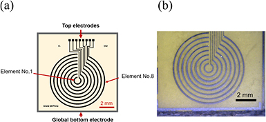
Figure 1. (a) Schematic diagram of the Tm-pMUT annular array based on PMN–PZT single crystal, and (b) image of the fabricated Tm-pMUT annular array.
Download figure:
Standard image High-resolution imageThe Tm-pMUT annular array based on a PMN–PZT single crystal was produced by a MEMS process (figure 2). The Tm-pMUT annular array was formed on 6 inch silicon (Si) wafer. A 1.13 µm-thick SiO2 layer was deposited by thermal wet oxidation at 1050 °C on a 6 inch Si wafer for electrical insulation (figure 2(a)). Twenty-nanometer titanium (Ti) and 180 nm platinum (Pt) layers were sputtered on the SiO2 layer as a bottom electrode; Ti functioned as the adhesive layer (figure 2(b)). A 5 µm-thick silver paste (ELCOAT, CANS, Japan) was applied between the PMN–PZT single crystal and the bottom electrode to bond the single crystal to the wafer (figure 2(c)). A PMN–PZT single crystal (CPSC 150-85; Ceracomp Co., Korea) was grown by the SSCG method and was of dimensions 20 × 20 × 0.3 mm3 and the material properties are shown in table 2 [34]. After the PMN–PZT single crystal layer was bonded, 200 nm-thick chromium (Cr) and 200 nm-thick gold (Au) layers were sputtered (figure 2(d)) to be used as a seed layer for nickel (Ni) deposition. A 58 µm SU-8 layer (SU-8 2100; MicroChem, USA) was then spin-coated and patterned by photolithography (figure 2(e)). The SU-8 layer was used as a mold for patterning a 20 µm-thick electroplated Ni (figure 2(f)) layer to be used as a hard mask for ICP etching. The SU-8 mold was later removed by acetone and sonication (figure 2(g)). After the Ni hard mask had formed, the Au/Cr/PMN–PZT layers were etched using a metal ICP-RIE system (FabStar +; TTL, Korea) to pattern the Tm-pMUT annular array (figure 2(h)). The Au/Cr/PMN–PZT layers were dry-etched to fabricate the Tm-pMUT annular array using boron trichloride/chlorine/argon (BCl3/Cl2/Ar) gases at a ratio of 5/3/2 (10/4/6 sccm). The RF power, bias power, and working pressure were fixed at 800 W, 350 W, and 2 mTorr, respectively. The optimization of ICP etching is discussed in section 3.3. ICP etching resulted in removal of a 30 µm PMN–PZT single crystal. Next, a 58 µm-thick SU-8 layer was spin-coated and patterned by photolithography to deposit the top electrode (Ti 20 nm/Pt 180 nm) by a lift-off process (figures 2(i) and (j)). After sputtering the top electrode, the SU-8 layer was removed using acetone and sonication (figure 2(k)). The spaces between the rings were filled with nonconductive epoxy (EPO-TEK 301; Epoxy Technology Inc., USA) and cured at room temperature for 24 h (figures 2(l) and (m)). The fabricated Tm-pMUT annular array was wire-bonded onto a printed circuit board (PCB) for characterization.
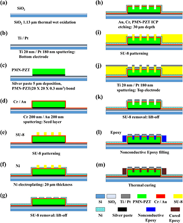
Figure 2. The fabrication process of the Tm-pMUT annular array based on a PMN–PZT single crystal.
Download figure:
Standard image High-resolution imageTable 2. Properties of the PMN–PZT single crystal [35].
Dielectric constant ( ) ) |
8000 |
| Dielectric loss (tan δ, %) | 0.5 |
| Curie temperature (TC, °C) | 150 |
| R-T transition temperature (TRT, °C) | 85 |
| Electro-mechanical coupling factor (k33) | 0.93 |
| Piezoelectric constant (d33, pC/N) | >2000 |
| Electro-mechanical coupling factor (k32)—(0 1 1) | 0.92 |
| Piezoelectric constant (d32, pC/N)—(0 1 1) | 2000 |
| Coercive electric field (EC, kV cm−1) | 3 |
| Mechanical quality factor (Qm) | 100 |
3. Characterization and investigation
3.1. Electrical characteristics of the Tm-pMUT annular array
After fabrication of the Tm-pMUT, the dipole domains of the PMN–PZT single crystal were misaligned because the processing temperature during the MEMS process exceeds 100 °C, which is higher than the phase transition temperature (85 °C) from rhombohedral to tetragonal phase of the PMN–PZT single crystal [34]. Therefore, the polling was performed to rearrange the misaligned dipole domains at room temperature. The poling conditions were 2 kV mm−1 DC for 2 h using a ferroelectric test system (Precision LC II; Radiant Technologies, USA). The polarized Tm-pMUT annular arrays based on PMN–PZT single crystals were electrically characterized using the ferroelectric test system. Figure 3 shows the hysteresis curve of element No. 7 in the Tm-pMUT annular array; the measured coercive field was 5.3 kV cm−1. This coercive field indicates that the Tm-pMUT can operate under 5.3 kV cm−1 [35].

Figure 3. Hysteresis curve of the Tm-pMUT annular array based on a PMN–PZT single crystal.
Download figure:
Standard image High-resolution imageThe resonance frequency of the Tm-pMUT annular array was measured using an impedance analyzer (4294A; Agilent Technology, USA) at the probe station to reduce external noise. Figure 4 shows the impedance and phase angle of element No. 7 in the Tm-pMUT annular array. The measured impedance value decreased as the element number was increased. This is because the area of the element increased as the element's number is increased, while the resistance decreased. The resonance frequencies of element No. 1 to element No. 8 were 2.62 MHz to 2.68 MHz; the average resonance frequency was 2.66 (±0.04) MHz. The anti-resonance frequencies of element No. 1 to element No. 8 were 3.20 MHz to 3.18 MHz; the average anti-resonance frequency was 3.18 (±0.03) MHz. All elements had similar resonance and anti-resonance frequencies because the frequencies are mainly determined by the thickness of the piezoelectric material, which can be calculated by  where c is the speed of sound in the active piezoelectric element and d is its thickness [36]. The measured effective EM coupling coefficient (
 ) was 30.05%, and was calculated by:
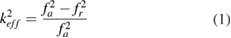
where fa is the anti-resonance frequency, and fr is the resonance frequency [37]. This value is significantly higher than the  of a bending-mode pMUT with a PZT thin film [32] and slightly higher than 25% of a thickness-mode annular array [38].
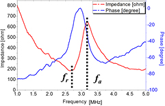
Figure 4. Impedance magnitude and phase angle of the seventh element.
Download figure:
Standard image High-resolution image3.2. Acoustic characterization of the Tm-pMUT annular array
Acoustic characterization of the Tm-pMUT annular array was performed using an acoustic intensity measurement system (AIMS; Onda Corp., USA) (figure 5). The Tm-pMUT annular array was activated using a function generator (WF 1946 2CH; NF Corp., Japan) and the transmitted signal from the device was captured by a hydrophone and amplifier (HNC-1000 & AH-2010; Onda Corp., USA). Amplified signals were measured by an oscilloscope (DSOX2004A; Agilent Technologies, USA) in a water bath containing deionized (DI) water. Before ultrasonic measurements, the Tm-pMUT annular array was spin-coated with a 5 µm thick Parylene layer to provide electrical insulation and waterproofing.

Figure 5. (a) Schematic diagram of the AIMS with the Tm-pMUT annular array and (b) photograph of the AIMS with the fabricated Tm-pMUT annular array.
Download figure:
Standard image High-resolution imageFigure 6 shows the measured acoustic characteristics of the Tm-pMUT annular array. The propagation of ultrasonic waves was visualized by AIMS during application of a 10 Vpp sine wave to the device at a center frequency of 2.66 MHz without beamforming. Figure 6(b) shows the axial acoustic intensity, which gradually increased to a peak at 7.24 mm and exponentially decreased as the axial distance increased. Figures 6(c) and (d) shows the 2D plane scan results at 7.2 mm from the Tm-pMUT; the maximum positive sound pressure was 40 kPa at the center. The annular nature of the Tm-pMUT array means that the ultrasound wave is focused at the center without beamforming.
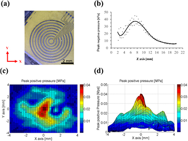
Figure 6. (a) Photograph of the Tm-pMUT annular array. (b) Measured peak negative pressure of the Tm-pMUT annular array without beamforming: XZ scanning result. (c) Measured peak positive pressure of the Tm-pMUT annular array without beamforming in the XY plane. (d) Measured peak positive pressure of the Tm-pMUT annular array without beamforming in the X plane at an axial distance of 7.2 mm from the array.
Download figure:
Standard image High-resolution image3.3. ICP etching of the PMN–PZT single crystal
3.3.1. Etch rate and etch selectivity of PMN–PZT and Ni.
The Ni layer (figure 2(f)) was used as a hard mask for ICP etching of PMN–PZT single crystals using the etching parameters in table 3. The initial etching parameters, such as RF power, bias power, gas flow rate, working pressure and etching time were selected based on information used for PMN-PT and PZT etching [39, 40], because the PMN–PZT single crystal consists of lead-based perovskite materials such as PZT and the electrostrictive relaxor ferroelectric PMN. Therefore, the characteristics of PMN–PZT single-crystal ICP etching are expected to resemble those of PMN-PT and PZT. As starting parameters for ICP etching characterization, RF power and bias power were set at 600 W and 250 W, respectively, which is 60% of the maximum power of the ICP etching equipment. The total gas flow rate was fixed at 20 sccm, and was mainly used for PZT etching [38]. The working pressure and etching time were set at 2 mT and 5 min, respectively, to ensure etching of sufficient material. For groups A, B, and C, the PMN–PZT single-crystal-etching properties were tested by varying the BCl3/Cl2/Ar gas flow rates. For groups D and E, the etch characteristics were measured by varying the RF power and the bias power with gas flow rates. Group F used the final optimized etching parameters for the Tm-pMUT based on the results of groups A to E. During the optimization process, the sidewall angle, etch rate, and etch selectivity ratio were used to determine the optimum etching parameters.
Table 3. ICP etching parameters of the PMN–PZT single crystal.
| Process no. | A-1–A-5 | B-1–B-5 | C-1–C-5 | D-1–D-5 | E-1–E-5 | F | |
| RF power (W) | 600 | 200–1000 | 600 | 800 | |||
| Bias power (W) | 250 | 250 | 50–450 | 350 | |||
| Gas flow rate (sccm) | Total | 20 | |||||
| BCl3 | 0 | 0–20 | 0–14 | 10 | 10 | ||
| Cl2 | 0–20 | 0 | 14–0 | 4 | 4 | ||
| Ar | 20–0 | 20–0 | 6 | 6 | 6 | ||
| Working pressure (mT) | 2 | ||||||
| Etching time (min) | 5 | ||||||
| Mask | Ni | ||||||
Figure 7(a) shows the effect of the Cl2/Ar gas mixture ratio on the etch rate and etch selectivity ratio between the PMN–PZT single crystal and Ni. The ratio of Cl2 gas was varied from 0 to 100% and that of Ar gas from 100 to 0%. The working pressure, RF power, bias power and total gas flow rate were fixed as listed in table 3. The maximum etch rate was 73.65 nm min−1 at a Cl2/(Cl2 + Ar) gas mixture ratio of 70% with an etch selectivity ratio of 3.35. In general, Cl2 is an important chemical etch factor for metals because the formation of metal chlorides is dependent on the concentration of atomic Cl for Cl2-based plasma etching [39]. If the Cl2 mixing ratio exceeds 70%, the etching rate decreases because excessive atomic Cl2 prevents the formation of metal chlorides. Ar+ ion is also essential in physical etching because Ar+ contacts the PMN–PZT single crystal surface and assists in plasma generation. After etching, PbClx, NbClx and TiClx metal fluorides remained on the surface of the PMN–PZT single crystal; this and the XPS data are discussed in section 3.3.3.
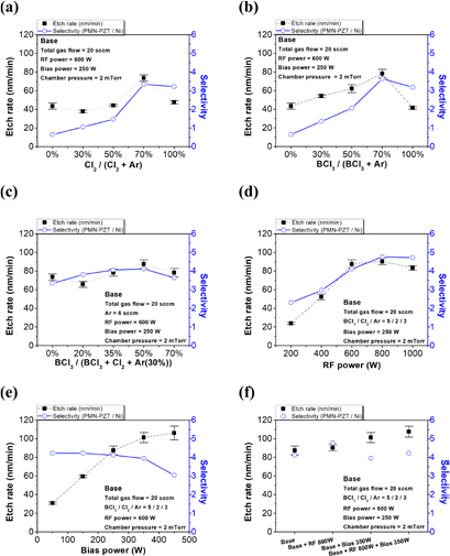
Figure 7. Etch rate and etch selectivity ratio of PMN–PZT and nickel (Ni) according to etching parameters.
Download figure:
Standard image High-resolution imageThe etch rate and etch selectivity ratio of the PMN–PZT single crystal and Ni according to BCl3/Ar gas mixture ratio are shown in figure 7(b). The ratio of BCl3 gas was changed from 0 to 100% and that of Ar gas from 100 to 0% in the same way as for the Cl2/Ar gas mixture. The working pressure, RF power, ICP bias power and total gas flow rate were fixed as listed in table 3. At a BCl3/(BCl3 + Ar) gas mixture ratio of 70%, the maximum etch rate and etch selectivity ratio were 78.38 nm min−1 and 3.65, respectively. These results are slightly higher than those in figure 7(a). BCl3 reportedly increases the etch rate and etch selectivity ratio due to B–O and BCl–O chemical bonds [40, 41]. Ar+ ions are used to remove nonvolatile etch products [42, 43]. B+ and BCl+ destroy the oxygen bonds of PMN–PZT single crystals and undergo reactions with B–O and BCl–O groups. Based on the etching characteristics of Cl2 and BCl3 (figures 7(a)–(c) shows the combined etch rate and etch selectivity ratio of PMN–PZT and Ni using various BCl3/Cl2/Ar gas mixtures. The proportion of BCl3 gas was changed from 0 to 70% and that of Cl2 gas from 70 to 0%. The proportion of Ar was fixed at 30% because this resulted in the highest etch rate (figures 7(a) and (b)). The working pressure, RF power, ICP bias power and total gas flow rate were fixed as listed in table 3. The maximum etch rate was 87.52 nm min−1 at a BCl3/(BCl3 + Cl2 + Ar (30%)) gas ratio of 50% (BCl3/Cl2/Ar = 5/2/3), with an etch selectivity ratio of 4.12. Therefore, the BCl3 plasma increased the etch selectivity ratio without reducing the etch rate of the PMN–PZT single crystal.
Figure 7(d) shows the effect of RF power on etch rate and etch selectivity. The RF power was changed from 200 to 1000 W while the gas mixture ratio was fixed at BCl3/Cl2/Ar = 5/2/3 (10/4/6 sccm), which was the optimal ratio (figure 7(c)). The chamber pressure and bias power were fixed as shown in table 3. The maximum etch rate and etch selectivity ratio were 90.37 nm min−1 and 4.77, respectively, at 800 W RF power. RF power is an essential factor in ion generation because the chemical reaction increased with increasing ion production. However, the etch rate and etch selectivity ratio were reduced at 800 W RF power because the average free path decreased and the levels of nonvolatile etch products increased.
Figure 7(e) shows the effect of bias power (50–450 W) on the etch rate and etch selectivity ratio. The gas mixture ratio, chamber pressure and RF power were fixed at BCl3/Cl2/Ar = 5/2/3, 2 mTorr, and 600 W, respectively (table 3). The maximum etch rate and etch selectivity ratio were 101.35 nm min−1 and 3.95, respectively, with 350 W bias power. Because the bias power determines the collision energy of the ions, the etch selectivity ratio decreased with increasing bias power. Because the etch rate in figure 7(e) is higher than that in figure 7(d), physical etching may predominate over chemical etching for PMN–PZT single crystals. Figure 7(f) shows the etch rates and etch selectivity ratios of a PMN–PZT single crystal and Ni for each case. The optimum etch rate and etch selectivity ratio were 107.6 nm min−1 and 4.22, respectively, at BCl3/Cl2/Ar = 5/2/3 (10/4/6 sccm), 800 W RF power, 350 W bias power, and 2 mTorr chamber pressure. Therefore, physical etching is dominant for the etch rate, and chemical etching is dominant for etch selectivity during ICP etching of PMN–PZT single crystal.
3.3.2. Effect of bias power on the sidewall angle.
A steep sidewall after PMN–PZT single crystal ICP etching is desirable to reduce interference between the adjacent Tm-pMUT annular array elements. Bias power is an essential factor for the etch rate of the PMN–PZT single crystal (figure 7(e). Thus, further study focused on the relationship between the sidewall angle and the bias power. Figure 8 shows scanning electron microscope (SEM) images taken at bias powers of 250, 350, and 450 W. The gas mixture ratio, chamber pressure and RF power were fixed, as shown in figure 7(e). As shown in figure 8, the sidewall angle increased up to 80.79° with 450 W bias power. This was because the power of ions colliding vertically increases as the bias power increases. High bias power is preferable to get a vertical structure, but high bias power also reduces the etch selectivity of PMN–PZT single crystal and Ni. The optimized bias power was 350 W in consideration of the dry etching process time and the thin Ni hard mask for fabricating the Tm-pMUT annular array. Since the sidewall angle with the 350 W bias power was 71.17°, each element of the Tm-pMUT annular array was sufficiently separated.
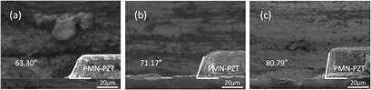
Figure 8. SEM images showing the sidewall angle of the PMN–PZT single crystal after ICP etching with various bias powers. (a) 250 W bias power, (b) 350 W bias power, and (c) 450 W bias power. Ni hard mask remains on the PMN–PZT single crystal.
Download figure:
Standard image High-resolution image3.3.3. X-ray photoelectron spectroscopy (XPS).
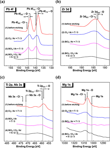
XPS analysis was performed to analyze the surface changes caused by chemical etching of the PMN–PZT single crystal (figure 9). PMN–PZT single crystal samples were investigated by XPS before and after ICP etching using Cl2/Ar = 7/3 (14/6 sccm), BCl3/Ar = 7/3 (14/6 sccm), and BCl3/Cl2/Ar = 5/2/3 (10/4/6 sccm) gas mixtures, respectively (figure 9(a)). These parameters were selected because they exert the greatest effects on PMN–PZT etching (section 3.3.1). During etching, the working pressure, RF power, and bias power were as in table 3.
Figure 9. XPS analysis of the PMN–PZT single crystal after ICP etching.
Download figure:
Standard image High-resolution image
The Pb 4f spectrum can be classified as Pb–O, Pb–Clx, and Pb. The binding energies of PbO and Pb–Clx are 137.6 and 138.9 eV, respectively [44, 45]. The chemical bond of Pb–O was dissociated by reaction with Cl gas, and the metal Pb peak appeared at the Pb 4f peak during etching because of the decreased Pb content. Figure 9(a) shows that the Pb–O peak was relatively low with the BCl3/Cl2/Ar = 5/2/3 (=10/4/6 sccm) gas mixture because of formation of a large number of amorphous layers on the PMN–PZT surface. This amorphous layer interferes with the binding energy measurement. After etching of the PMN–PZT single crystal, the core binding energy of Pb 4f was shifted by Δx (=0.7 eV) because Pb was oxidized. As shown in figure 9(b), Zr can also be classified into Zr–O and Zr–Cl, and the peaks at 183.3 and 184.5 eV correspond to Zr–O and Zr–Cl, respectively [46, 47]. After etching, the Cl2/Ar = 7/3 (14/6 sccm) gas mixture showed the highest Zr–O peak intensity; the BCl3/Cl2/Ar = 5/2/3 (=10/4/6 sccm) gas mixture exhibited the lowest peak (figure 9(b)). The core binding energy of Zr 3d was increased by 0.5 eV after etching because of oxidation of Zr. Ti is a constituent of perovskite PZT and can associate with –O and –Cl. The binding energies of Ti–O and Ti–Cl are 458.5 and 459.5 eV, respectively [48, 49]. Figure 9(c) shows that the Ti–O binding energy peak reached Δz (0.8 eV). The intensity of the Ti–O peak was lowest with the BCl3/Cl2/Ar = 5/2/3 (10/4/6 sccm) gas mixture. The Nb can also be bound in the forms of Nb–O, Nb–Cl. After etching of the PMN–PZT single crystal, the binding energy peak of Nb–O and Nb–Cl occurred at 470.8 and 474.0 eV, respectively [50]. The intensity of the Nb–O bond peak was lowest with a BCl3/Cl2/Ar = 5/2/3 (10/4/6 sccm) gas mixture. Mg can bind in the forms of Mg–O and Mg–Cl. The binding energies of Mg–O and Mg–Cl were 1306.0 eV and 1307.5 eV by XPS analysis. Figure 9(d) shows that the intensity of the Mg–O peak was highest with the Cl2/Ar = 7/3 (14/6 sccm) gas mixture and lowest with the BCl3/Cl2/Ar = 5/2/3 (10/4/6 sccm) gas mixture.
The main reason for the decrease in the binding energy peak intensity after ICP etching of the PMN–PZT single crystal is physical etching by the cation [51]. ICP etching results in the formation of an amorphous layer on the PMN–PZT surface [52], which interferes with XPS and reduces the binding energy peak intensity.
4. Discussion
The resonance frequencies of pMUT and cMUT are inversely proportional to the diaphragm diameter. The higher the resonance frequency, the smaller the diaphragm diameter. There is a minimum allowable diaphragm diameter (achievable high frequency) due to the minimum possible resolution of photolithography for a pMUT array, and this limits the attainable frequency and compactness of the pMUT array. In the case of the Tm-pMUT, the resonance frequency is determined by the thickness of the piezoelectric layer, unlike the bending mode. Therefore, the minimum resolution of photolithography does not limit the maximum possible frequency or the compactness of the pMUT array. Thus, Tm-pMUT facilitates production of high-frequency pMUTs of simple array design.
In this study, a MEMS technique was developed to fabricate Tm-pMUT annular arrays using brittle PMN–PZT single crystals, as a circular element cannot be fabricated using a dicing method. The ICP etching parameters of the PMN–PZT single crystal were investigated to pattern the circular shape of the Tm-pMUT annular array. ICP etching techniques can also be utilized to fabricate next-generation MEMS devices with PMN–PZT and other piezoelectric single-crystal materials because fabrication of more diverse patterns, including curves, is feasible.
The coercive electric field of the fabricated PMN–PZT single-crystal-based Tm-pMUT annular array was 5.3 kV cm−1, which suggests its feasibility for high-voltage and high-power applications. As explained above, 2D scanning of the acoustic pressure was performed 4–25 mm from the Tm-pMUT annular array after water-proofing at the center frequency of 2.66 MHz. The center frequency was measured in air, and the frequency is expected to be lower with the Parylene layer in the water. The maximum acoustic pressure is thought to occur at the geometric center of the annular array, but the actual peak pressure was slightly outside of the array center. This is because the elements of the Tm-pMUT annular array form an incomplete ring (figure 1) that is open due to the top-electrode connection. This can be improved by a more accurate design and use of a beamformer. Controlled beamforming and acoustic intensity will enable use of the proposed Tm-pMUT annular array based on PMN–PZT single crystals for various biomedical applications, such as cell and tissue stimulation.
5. Conclusions
In this study, a PMN–PZT single-crystal-based Tm-pMUT annular array was fabricated by MEMS technology. Patterning of the circular PMN–PZT single crystal was facilitated by ICP dry etching of the PMN–PZT single crystal, and would not be possible by a conventional dicing method. To efficiently pattern the PMN–PZT, ICP etching conditions were optimized using SEM micrographs and XPS analysis. The optimized ICP condition was a BCl3/Cl2/Ar = 5/2/3 (=10/4/6 sccm) gas mixture, 800 W RF power, 350 W bias power, and 2 mTorr chamber pressure. Under these conditions, the etch rate of the PMN–PZT layer was 107.6 nm min−1 and the etch ratio was 4.22.
The Tm-pMUT annular array has several advantages, such as high spatial efficiency, high acoustic intensity, and high effective EM coupling coefficient. The fabricated Tm-pMUT annular array has eight circular ultrasonic transducer elements within 1 × 1 cm2. The average resonance frequency, average anti-resonance frequency, and effective EM coupling coefficient of the device were 2.66 (±0.04) MHz, 3.18 (±0.03) MHz, and 30.05%, respectively. The Tm-pMUT annular array generated a high positive sound pressure of 40 kPa without a beamformer. Because a beamformer can further improve the ultrasound intensity, the proposed Tm-pMUT has the potential to generate higher acoustic intensity for use in various biomedical applications.
Acknowledgments
We thank the Center for Core Research Facilities of DGIST for technical support. This research was supported by the Civil & Military Technology Cooperation Program through the National Research Foundation of Korea (NRF) funded by the Ministry of Science and ICT (No. NRF-2014M3C1A9060874), the Korea Evaluation Institute of Industrial Technology (KEIT) funded by the Ministry of Trade, Industry, and Energy (MOTIE) (NO. 10074267), and the DGIST R&D Program of the Ministry of Science and ICT (17-BD-0404). The work at YU was supported by internal R&D program of YU.