
Abstract
Polymer based MEMS and microfluidic devices have the advantages of mechanical flexibility, lower fabrication cost and faster processing over silicon based ones. Also, many polymer materials are considered biocompatible and can be used in biological applications. A valuable class of polymers for microfabricated devices is piezoelectric functional polymers. In addition to the normal advantages of polymers, piezoelectric polymers can be directly used as an active material in different transduction applications. This paper gives an overview of piezoelectric polymers based on their operating principle. This includes three main categories: bulk piezoelectric polymers, piezocomposites and voided charged polymers. State-of-the-art piezopolymers of each category are presented with a focus on fabrication techniques and material properties. A comparison between the different piezoelectric polymers and common inorganic piezoelectric materials (PZT, ZnO, AlN and PMN–PT) is also provided in terms of piezoelectric properties. The use of piezopolymers in different electromechanical devices is also presented. This includes tactile sensors, energy harvesters, acoustic transducers and inertial sensors.
Export citation and abstract BibTeX RIS
1. Introduction
A piezoelectric material can have an electrical field induced across its boundaries when a mechanical stress is applied on it, or vice versa. This piezoelectric effect was first discovered by the Curie brothers in 1880 [1]. In the first half of the 20th century, different macro-scale electromechanical transducers were developed based on piezoelectric materials which were more directed to military and marine applications [2]. Since the idea of integrated microelectromechanical systems (MEMS) emerged in the 1980s, it has been realized that piezoelectric materials can add an advantageous functionality for building such systems [3]. This led to different piezoelectric MEMS (or, briefly, piezoMEMS) devices that are commonly used now in the automotive industry, smart phones and other everyday applications [4]. These microsystems are mainly based on inorganic piezoelectric materials because of the well established experience of the silicon microelectronic industry which was the core motive for the emerging MEMS technology. However, the usage of such inorganic materials poses some challenges such as the high temperature processing required for thin film fabrication and polar reorientation [4], the toxicity of lead-containing materials like lead zirconate titanate (PZT) and the need for high cost manufacturing capabilities for fabrication. To counter the inorganic materials' complexity, there has been a new trend of exploring polymeric materials in the MEMS field since the 1990s [5].
The use of polymer materials in different MEMS and microfluidics applications had an increasing interest due to the advantages that polymer materials have. These advantages include the mechanical flexibility which is necessary in certain applications compared to silicon. Also, polymer based devices are commonly less expensive in terms of material cost and processing technology which includes soft lithographic techniques [6] that do not commonly require advanced microfabrication facilities. The commonly used polymers in many microfabricated devices are generally electrically insulating and mechanically flexible compared to inorganic materials. Yet, there are many polymers that have additional properties that make them distinctly advantageous in certain applications. These functional polymers include conductive [7], electroactive [8] and semiconducting [9] polymers. There are different review papers about polymer MEMS [5] and microfluidics [6, 10] devices in the literature which are referenced here for the reader.
Electroactive polymer (EAP) materials mechanically deform by the application of an electrical stimulus. They can be divided into electronic and ionic EAPs according to the operating principle [8]. In an electronic EAP, the electromechanical transduction is due to the electrostatic manipulation of dipoles while it is due to the manipulation of ions within the ionic EAP. Tiwari and Garcia [11] recently reviewed the main type of ionic EAPs, which is the ionic polymer–metal composites, in terms of fabrication and characterization. We here focus on piezoelectric polymers which are categorized as electronic EAPs. Piezoelectric polymers can be used to fabricate piezoMEMS at a lower cost and potentially easier processing than their inorganic counterparts. This paper provides a review of the different piezoelectric polymers that can be used in the MEMS field for sensing and actuation in terms of their operating principles and properties of the different materials. This includes three main categories: bulk polymers, piezoelectric polymer composites and voided charged polymers. Because the piezoelectricity term is not as commonly treated in polymers as in piezoelectric ceramics or inorganic materials, an introductory section about piezoelectricity is provided in order to identify the common definitions and terminologies which will be readdressed in each piezoelectric polymer type with proper specific definitions related to the operating principle of each type. State-of-the-art piezoelectric polymer materials used in MEMS from 2009 until 2013 are also reviewed with a focus on material properties, processing techniques and applications specifically for sensing and energy harvesting. A comparative analysis between the different piezoelectric materials and their most common inorganic counterparts for MEMS is also presented. The review is concluded with remarks on future trends and challenges for piezopolymers in the field of microfabrication.
2. Piezoelectricity
2.1. Definition of piezoelectricity
The term 'piezoelectricity' is used to describe dielectric materials that produce electrical charges across their boundaries due to the application of a mechanical stress, which is called the direct piezoelectric effect [12]. The indirect (or converse) piezoelectric effect happens when the material is subjected to an electrical field which causes a mechanical strain of the material. In piezoelectric materials, the relationship between induced charges per unit area and the applied stress is linear and reversible. In inorganic piezoelectric crystalline materials, such as aluminum nitride (AlN) [13], this phenomenon happens due to the arrangement of ions in the crystal structure of the dielectric material. The internal polarization of the material changes linearly with the applied stress, causing an electrical field to develop across the material boundary. Such crystal structures are said to lack inversion symmetry [14]. For an AlN thin film, the piezoelectric coefficient is highly dependent on the crystal orientation of the film, which cannot be changed after deposition. Alternatively, in a ferroelectric material, such as lead zirconate titanate (PZT), the internal dipoles of the material can be reoriented by the application of an external electric field, leaving a remanent polarization at zero applied electric field [3]. This remanent polarization also changes with the applied stress and this is where piezoelectricity takes place. So every ferroelectric material is piezoelectric but not every piezoelectric material is ferroelectric.
2.2. Analytical formulation of piezoelectric effect
Based on thermodynamic potential and energy exchange principles [12], the piezoelectric phenomenon can be formulated with the following equations:


where D is the electric displacement; E is the electric field; σ is the stress; δ is the strain; εo is the free space electric permittivity; d is the piezoelectric coefficient; εσ is the material's electric relative permittivity (or dielectric constant) matrix at a constant stress and SE is the material's mechanical compliance matrix; I and J are indices with values from 1–6 while i and j are indices from 1–3. D and E are (3 × 1) tensors indicating the three coordinate directions x, y and z. σ and δ are (6 × 1) tensors indicating the normal stresses or strains (elements from 1–3) and shear stresses or strain (elements from 4–6).
2.3. The piezoelectric coefficients and modes
The piezoelectric strain coefficient diJ is a (3 × 6) tensor which is defined as the electric polarization generated in direction i in the material per unit mechanical stress of index J applied to it or the induced mechanical strain of index J per unit electric field applied in direction i. The piezoelectric d coefficient has the unit of coulombs/newton or meters/volt. There are other piezoelectric coefficients that are defined in different ways such as the piezoelectric stress coefficient e, the piezoelectric voltage coefficient g and the inverse piezoelectric strain coefficient h [15]. They are all related and can be derived from one another but we will restrict ourselves in this review to the d coefficient in order to get a useful insight comparing the different materials.
In most of the piezoelectric materials, there are only 3 or 4 piezoelectric coefficient elements and the rest of the elements are zero in the (3 × 6) tensor. The two popular and common elements in most piezoelectric materials are d31 and d33. The d33 coefficient is called the longitudinal coefficient, which describes the electric polarization generated in the same direction as the stress applied. The d31 coefficient is called the transverse coefficient, which describes the electric polarization generated in a direction perpendicular to the direction of the applied stress. In piezoelectric MEMS, it is common to use the terminology 31 mode and 33 mode to distinguish the two transduction mechanisms. Figure 1 illustrates graphically the two modes. It also should be noted that the effective piezoelectric coefficient of a thin film is different from that of a bulk substrate of the same material due to the quality of crystal orientation of the grown thin film and the boundary conditions that the substrate imposes on the grown thin film. The subscript f is added for the diJ, f coefficient to indicate the effective piezoelectric coefficient of the thin film, which is what is measured practically and can be related to the diJ and the SIJ constants [4].

Figure 1. The piezoelectric transduction modes.
Download figure:
Standard image High-resolution image2.4. The electromechanical coupling
A useful parameter to compare different piezoelectric materials is the electromechanical coupling coefficient denoted as k. The coupling coefficient is a measure of the conversion efficiency between mechanical and electrical energy using the piezoelectric material. It takes the same indices as the piezoelectric coefficient d and is formulated as [15]
3. Piezoelectricity in polymers
There are different polymer categories that can be considered piezoelectric. Figure 2 shows a graphical representation of the different types. The first category of piezoelectric polymers is the bulk polymer. These are solid polymer films that have the piezoelectric mechanism through their molecular structure and its arrangement. The second category is the piezoelectric composite polymer. These are polymer structures with integrated piezoelectric ceramics from which the piezoelectric effect is generated. These composites make use of the mechanical flexibility of polymers and the high electromechanical coupling of the piezoelectric ceramics. The third type is the voided charged polymer, a radically different type of piezoelectric polymer than the first two categories. This is a polymer film in which gas voids are introduced and surfaces are charged in a way to form internal dipoles. The polarization of these dipoles changes with the applied stress on the polymer film (i.e. has a piezoelectric response). Each of these three classes of polymers is discussed in the following subsections in detail followed by state-of-the-art materials and applications.

Figure 2. Schematic diagrams of piezoelectric polymer types: (1) bulk piezopolymers: which are divided into amorphous dipolar polymers and semi-crystalline polymers, (2) piezoelectric/polymer composites, two examples of which are piezoelectric particles embedded in polymer or piezoelectric pillars inside polymer (also named (1–3) composites) and (3) voided charged polymers: polymers with air voids with charged surfaces in polar form.
Download figure:
Standard image High-resolution image3.1. Bulk piezoelectric polymers
Bulk piezoelectric polymers have a piezoelectric effect due to the molecular structure of the polymer and its orientation. There are two types of bulk polymers that have different operating principles: the semi-crystalline polymers and amorphous polymers. A detailed review of both types and their theory and piezoelectric properties is presented by Harrison in [15]. In these two types, there are structural requirements that should exist for a bulk polymer material to be piezoelectric. First, the molecular structure of the polymer should inherently contain molecular dipoles. Second, these dipoles can be reoriented within the bulk material and kept in their preferred orientation state. This reorientation is done through a process called poling, which will be explained in section 3.1.2.
3.1.1. Semi-crystalline piezoelectric polymers
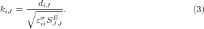
There is a class of polymer materials that has a semi-crystalline structure such as polyvinylidene fluoride (PVDF) [16], polyamides, liquid crystal polymers [15] and Parylene-C [17]. Semi-crystalline polymers operate in principle similar to piezoelectric inorganic materials.
A simplified 2D schematic is shown in figure 3 to explain the concept. The positively and negatively charged ions (or polar group in polymers) are arranged in a crystalline form to cause the change in polarization with applied stress. In figure 3(a), a square structure with positive and negative ions' arrangement is hypothetically placed under compressive stress. For this structure, the equivalent center of charge of the positive and negative ions is still at the same point and there is no polarization change due to the force applied. On the other hand, for a 2D hexagon with the ion arrangements shown in figure 3(b), the applied stress induces a change in the center of charge of the positive and negative ions, which means a change in the polarization that causes an effective electrical field.
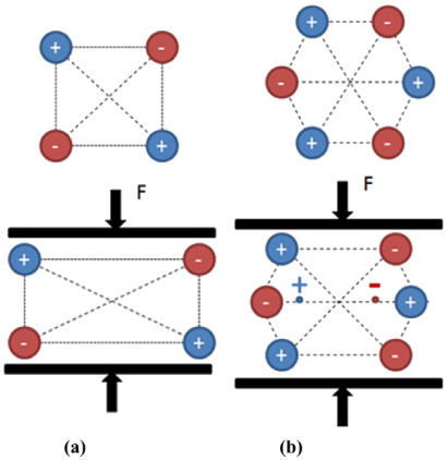
Figure 3. Examples of 2D crystal structures: non-piezoelectric (a) square and piezoelectric (b) hexagon.
Download figure:
Standard image High-resolution imageThe bulk of a semi-crystalline polymer is not a single crystal structure. It can be viewed as randomly oriented microscopic crystals distributed within an amorphous bulk. In order to get an effective piezoelectric response out of such a material, there should be an ability to reorient these crystallites and keep them in the preferable orientation, which is done by the poling process.
3.1.2. Poling of polymers and the enhancement of the piezoelectric effect
The process of poling is the process of reorientation of the crystallites (or, generally speaking, the molecular dipoles) within the polymer bulk medium through the application of a high electric field at an elevated temperature. In order to sustain the orientation state of the molecular dipoles, the temperature of the material is cooled down in the presence of the electric field. There are two methods that are commonly used in poling polymers: electrode poling and corona poling, illustrated in figure 4.
Figure 4. Piezoelectric polymer poling systems: (a) corona poling and (b) electrode poling.
Download figure:
Standard image High-resolution imageThe electrode poling, shown in figure 4(b), is simpler than the corona poling. Conductive electrodes should be deposited or pressed on both sides of the polymer film to apply the high voltage across the polymer. The voltage applied could be DC, AC sinusoidal or triangular low frequency wave forms [16]. For different bulk piezoelectric polymers, the applied electric field reported is in the range from 5–100 MV m−1 [16–19]. This strong electric field could cause the polymer to break down; that's why the poling process should be done in a vacuum chamber [18] or immersed inside an electrically insulating fluid [17, 19]. The final quality of the alignment of crystallites (and consequently the piezoelectric coefficient d) depends on the following factors: the strength and time of the applied electrical field, the value and degree of uniformity of the temperature applied on the polymer and the degree of contamination or voids between the electrodes and the polymer surface. For some materials like PVDF, mechanical stretching of the polymer film during the poling process enhances the quality of the crystallite alignment [15].
Unlike the electrode poling process, corona poling requires only one side of the polymer film to be covered with an electrode. As shown in figure 4(a), a conductive needle subjected to very high voltage Vc (8–20 kV) is placed on top of a grid at a much lower DC voltage Vg (0.2–3 kV), which is on top of the piezoelectric polymer in a dry air or argon medium [16, 18]. The gas molecules around the tip get ionized and accelerated towards the surface of the piezoelectric polymer. The grid position and applied voltage controls the amount of deposited charges on the polymer surface, which is the way to control the applied electrical field across the polymer. The hot plate introduces heat for better control of the poling.
As for the temperature, the required temperature for both methods does not go beyond 300 °C in all cases found in the literature. This is much lower than that required for PZT processing temperatures, which can be as high as 1200 °C [4]. Although corona poling is more complicated than electrode poling, corona poling can compensate for the polymer film surface roughness and does not require electrode deposition.
There are other methods for poling which are less commonly used and reported such as electron beam poling [20], where electron beam irradiation is used to deposit electrons on the surface of the piezoelectric polymer which causes the reorientation of the dipoles, similar to the corona poling method. One advantage of such a method is the ability to locally pole certain areas of the film by direct patterning with the focused electron beam. The reason for not being commonly used, however, is that it causes chemical modification and degrades the material under poling [21]. Another interesting charging method is the use of soft x-rays for ionization [22], which is mainly useful for voided charged polymers. This method will be discussed more in the relevant section.
3.1.3. Amorphous piezoelectric polymers
The piezoelectric effect can be found in a polymer that does not have long range order (in other words non-crystalline) if its molecular structure contains molecular dipoles. Examples of such polymers include polyimide [18, 23] and polyvinylidene chloride (PVDC) [15]. If poling is done at a temperature a few degrees greater than the glass transition temperature of the polymer, these dipoles can be effectively aligned with the applied electric field. After cooling, these dipoles are not in the same thermal equilibrium state as their counterparts in semi-crystalline polymers. The remanent polarization Pr after the poling process is linearly dependent on the poling electric field Ep and the resultant piezoelectric coefficient d31 can be determined from the following equation [15]:

where ν is the mechanical Poisson's ratio, Y is Young's modulus of the polymer and ε∞ is the material's permittivity at high frequencies. The dielectric relaxation strength of a polymer Δε is defined as the change in the dielectric constant of the polymer when heated from a temperature below the glass transition temperature Tg to a temperature higher than Tg [18].
3.2. Polymer piezoelectric composites
A piezoelectric polymer composite (or a piezocomposite) is a polymer material with embedded inorganic piezoelectric material. In our discussion here of what we call a piezocomposite, the polymer is assumed to be not electromechanically active. Meaning, a composite with a polymer matrix material like PVDF is not what we intend to review in this section. The advantage of mixing piezoelectric ceramics with polymers is to combine the advantages of both materials, which include the higher coupling factor and dielectric constant of ceramics and the mechanical flexibility of polymers. Piezocomposites are also the material of choice for acoustic devices because of the polymer's low acoustic impedance and fewer spurious modes [24]. Arrangement of ceramic/polymer composites can have many different combinations [24]. Arranged or randomly scattered rods in polymer bulk films are commercially available from companies like Smart Material, which are classified as (1–3) composites. Another approach is to impinge microscale or nanoscale particles inside a polymer matrix. Depending on the connectivity between the particles, such a composite could be (0–3) if the particles are completely separated and surrounded by the polymer material, or it could be (3–3) if the particles are in contact [25]. The rods or particles embedded in a polymer are the most common arrangements for composites used in millimeter to micrometer scale electromechanical devices. Different analytical and numerical models have been developed to estimate the material properties of such composites [25–27]. Although such models are useful in designing and predicting the different electrical, mechanical and electromechanical properties of piezocomposites, they are rarely used by experimentalists when new composites are developed. This is mainly due to the complexity of the experimental composites where multiple fillers, for example, are used in the polymer matrix [28]. That is why it is rare to find a developed composite material with measured values of dielectric constant, Young's modulus and piezoelectric coefficients all reported. This introduces difficulties in comparing such properties of the different materials, as will be seen later in the state-of-the-art materials.
3.3. Voided charged polymers
In simple terms, voided charged polymers (sometimes called cellular polymers) are polymer materials that contain internal gas voids. When the polymer surfaces surrounding the voids are charged, the voided charged polymer behaves like a piezoelectric material, coupling electrical and mechanical energy. Such structures can have a high piezoelectric coefficient d33 which can reach up to 20 000 pC N−1 in some cases [29], a comparably higher value than that of piezoceramics.
This structure was first invented by Gerhard Sessler in the early 1960s [30] when he developed a charged polymer device to be used as a microphone. It was only viewed and named as 'space charged electrets'. It was not until the late 1980s that researchers accepted the concept of treating the space charged electrets as a 'black box' and investigated the piezo- and pyroelectricity of such films [31].
The concept of piezoelectricity in voided charged polymers (also known as ferroelectrets or piezoelectrets) is illustrated in figure 5. Starting with a polymer film with embedded air voids, internal charging of voids can be done through electrical poling explained earlier in section 3.1.2. When a large electric field is applied across the film, gas molecules in the voids get ionized and opposite charges are accelerated and implanted on each side of the voids, depending on the applied electric field direction [31]. Such 'artificially' embedded dipoles respond externally to an applied electrical field or mechanical force similar to piezoelectric material. Instead of ion displacement in a crystalline structure of a regular piezoelectric material, deformation of the charged voids is the cause of the piezoelectric effect.
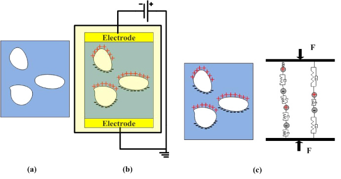
Figure 5. Illustration of piezoelectricity in voided charged polymers: (a) the voided polymer before charging, (b) the electrode poling process for forming the trapped dipoles and (c) illustrative simple model to explain the piezoresponse of VCP.
Download figure:
Standard image High-resolution image3.3.1. Factors affecting the piezoelectric coefficient in voided charged polymers
Conceptually, voided charged polymers (VCP) behave like piezoelectric materials; however, the piezoelectric coefficient in such a hybrid material depends on factors different from that of regular piezoelectric materials. First, there are factors related to the voids. The density and shape of the voids affects the distribution of the final formed dipoles. Also, the type and pressure of gas inside the voids affects the amount of ionization occurring during the poling process. These factors affect the value of the piezoelectric coefficient.
3.3.1.1. Frequency dependent piezoelectric response of VCPs
There is another factor that is more dominantly influential on VCPs than regular piezoelectric materials, which is the dependence of the piezoelectric coefficient on the frequency of applied force or electric field. This can be understood if the VCP is viewed as a structure of charges suspended with different springs and dampers [32] as shown in figure 5(c). Such a complicated structure has a resonant mechanical response; therefore, the total displacement of the structure changes with the applied frequency and consequently the generated electric charges will be different. This variation required researchers to define two piezoelectric coefficients: quasistatic and dynamic piezoelectric coefficients [32]. It should be noted that the frequency dependence of the piezoelectric coefficient exists in other types of piezoelectric materials; however, it is not dominant enough to be considered in designing micrometer scale devices. For example, an experimental study of the piezoelectric coefficient of PVDF showed no significant change in g31, g32 and g33 coefficients at a frequency range of 400 kHz [33].
3.3.1.2. Quasistatic and dynamic piezoelectric coefficients of VCPs
The quasistatic piezoelectric coefficient d is defined as the electric charge density generated per unit stress (or pressure) applied across the material at zero or very low frequency of a few Hz. The quasistatic piezoelectric coefficient is the value that is commonly reported and compared with other regular piezoelectric materials. The dynamic piezoelectric coefficient is studied by measuring the charge density per unit stress (or pressure) applied at a range of frequencies. The maximum dynamic piezoelectric coefficient matches the resonance of the VCP film. As an illustration, the piezoelectric response of commercial cellular polypropylene is shown in figure 6 from [29]. For details about the experimental setup for measuring these values the reader can refer to the reference. As seen from figure 6(a), the value of the quasistatic d33 changes with the static pressure and also with whether the film is preloaded with a stretched force or not. Figure 6(b) shows how the d33 value changes with the frequency of the applied dynamic pressure, showing resonance at 300 kHz.
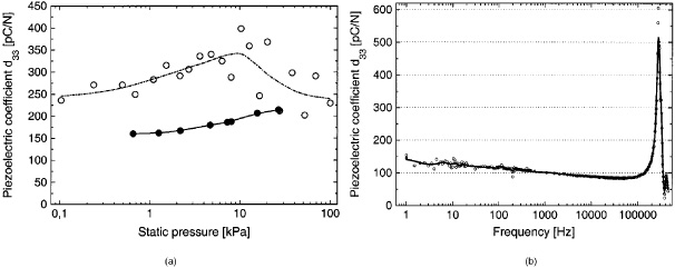
Figure 6. Quasistatic and dynamic piezoelectric d33 coefficient for cellular polypropylene: (a) quasistatic coefficient of stretched films (circles) and non-stretched films (dots) at different static pressures and (b) interferometric measurement of dynamic piezoelectric coefficient of a non-stretched film © 2004 IEEE. Reprinted, with permission, from [29].
Download figure:
Standard image High-resolution image4. State-of-the-art piezoelectric polymers
This section reviews the state-of-the-art piezopolymers in terms of their material properties and processing techniques. Also, it reviews the different key applications where these materials have been used within the last five years. There is also an emphasis on potential materials that could be useful for future electromechanical applications.
4.1. Bulk piezoelectric materials
In this section, the discussion is focused on three piezoelectric polymers that have been used in MEMS applications, which are PVDF and its various copolymers, Parylene-C and Polyimide. Table 1 summarizes the material properties for the three materials. The molecular structures of the different polymers are shown in figure 7.
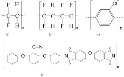
Figure 7. Molecular structure of selected bulk piezoelectric polymers. (a) PVDF, (b) PVDF-TrFE, (c) Parylene-C and (d) Polyimide (β-CN) APB/ODPA.
Download figure:
Standard image High-resolution imageTable 1. Material properties for bulk piezopolymers.
| PVDF [12, 15, 34] | PVDF–TrFE [12, 15, 19, 34, 35] | Parylene-C [17, 36, 37] | PI (β-CN) APB/ODPA [15, 18] | ||
|---|---|---|---|---|---|
| Density | (kg m−3) | 1800 | 1900 | 1290 | 1420 |
| Young's modulus Y | (GPa) | 2.5–3.2 | 1.1–3 | 2.8 | 2–3 |
| Dielectric constant εr | 12 | 12 | 3.15 | 4 | |
| Dielectric loss tanδe | 0.018 | 0.018 | 0.01 | ||
| Mechanical loss tanδm | 0.05 | 0.05 | 0.06 | 0.06 | |
| d33 | (pC N−1) | 13–28 | 24–38 | 2.0 | 5.3–16.5 |
| d31 | (pC N−1) | 6–20 | 6–12 | ||
| k33 | 0.27 | 0.37 | 0.02 | 0.048–0.15 | |
| k31 | 0.12 | 0.07 | |||
| Maximum use temperature | (°C) | 90 | 100 | 220 |
4.1.1. PVDF and PVDF copolymers
PVDF is the most commonly used and cited piezopolymer in electromechanical devices. This is because it has the largest piezoelectric coefficient, 20–28 pC N−1, compared with other bulk polymers [15]. PVDF is a semi-crystalline polymer which is synthesized by the polymerization of H2C = CF2 monomers (see figure 7(a)). A defect in the connected polymer chain occurs when two CF2 groups or CH2 groups are connected. Increased defects in the polymeric chain increase the polarity of the semi-crystalline polymeric film, which consequently increases the piezoelectric response [16]. That's why there are different synthesis methods that have been developed to enhance the crystal orientation such as the addition of trifluoroethylene (TrFE) (figure 7(b)) [35], carbon black [38] or carbon nanotubes [39]. There is also research done on the addition of piezoelectric inorganic particles with PVDF to selectively enhance the piezoelectric or the pyroelectric response of the material through a specific poling mechanism [40]. This includes BaTiO3 [41], PZT [40] or ZnO [42].
As for fabrication, already poled PVDF and PVDF–TrFE films of different thicknesses are commercially available [34]. Such films have been used to fabricate MEMS pressure sensors [43] and an energy harvester [44]. In this case, the device dimensions are usually in the 100s of microns to millimeter range and laser cutting is the method of choice for patterning in that range [44, 45]. For MEMS scale applications, the material is dissolved and spin coated. As shown in table 2, methyl ethyl ketone (MEK) (also called 2-butanone) is the most commonly used solvent for PVDF and its copolymers. For patterning and etching, oxygen dry plasma is used, which is a common method for etching most polymers.
The poling process is always a key step in PVDF fabrication for a high piezoelectric response. However, the spin coating process by itself acts like mechanical stretching and enhances the β-phase crystal orientation [35]. The thinnest spin coated film found in the literature is 1 μm [35]. In their study, no poling was performed and this 1 μm film showed a piezoelectric response two times higher than a 6 μm film fabricated with the same process. In addition, the piezoelectric coefficient in this case is higher than the 28 pC N−1 value of the thick films. This method simplifies the fabrication and increases the advantages of using PVDF. Another method that also showed a high piezoelectric coefficient of 72 pC N−1 is the nanoimprinted sub-20 nm PVDF–TrFE nanograss [46, 47]. However, this high value is not uniform across the whole array of nanograss pillars, which could lead to unreliable repeatability. An even higher piezoelectric response has been achieved by recrystallization of the PVDF–TrFE film through annealing before imprinting the nanograss on the film [48]. A tactile sensor device was demonstrated using the PVDF–TrFE nanograss [48].
4.1.2. Parylene-C
Parylene is commonly used as an electrically insulating or encapsulation material in MEMS and microfabrication. This is due to its biocompatibility, chemical resistance and, more importantly, its unique vapor deposition method. This deposition method allows conformal coating over any surface, regardless of its porosity. The physical deposition method for Parylene consists of three steps: evaporation, pyrolysis and deposition [49]. First, the raw material in dimer form is heated in vacuum to a temperature of 150–200 °C to form a vapor. In the pyrolysis step, the vapor is broken into monomers when heated to temperatures of 600–700 °C. Finally, the monomer gas is polymerized on the target surfaces at room temperature [49]. The Parylene-C molecular structure, shown in figure 7(c), has a molecular dipole due to the single chlorine atom in the benzene ring [17]. Recently, the piezoelectric response of semi-crystalline Parylene-C has been investigated and was also used to fabricate d33 based piezoelectric cantilevers [37] and microphones [50]. The reported piezoelectric coefficient of Parylene-C is 2 pC N−1, which is very low and this raises questions for the applicability of the material for a useful piezoelectric element. More effort is still needed to increase the piezoresponse and make use of the fabrication advantages of Parylene-C.
Table 2. Key aspects of different fabrication methods and poling conditions used for bulk piezopolymers and piezo composites.
| Material | Reported d | Fabrication method | Poling conditions |
|---|---|---|---|
| Piezopolymers | |||
| PVDF–TrFE [19] | d33, f = 0.07–1 pC N−1 |
• Replica molding for multiple films of 30 μm total thickness • Methyl ethyl ketone (MEK) solvent used for SU-8 on Si mold • Tetrahydrofuran (THF) solvent used for COC mold | DC electrode poling • Electric field: 70 MV m−1 • Temperature: 90 °C for 30 min |
| PVDF–TrFE [35] | d33, f = 38–74 pC N−1 |
• Spin coated PVDF dissolved in MEK for 1 and 6 μm | No poling |
| • Etched using oxygen plasma etching with a photoresist mask | |||
| PVDF [51] | • Electrospinning of PVDF dissolved in acetone/N,N-dimethylformamide | No poling | |
| • Shape of patterned structure: fibers with 100–800 nm diameter | |||
| PVDF–TrFE [52, 53] | • Spin coated PVDF dissolved in RER500 solvent (ethyl lactate/MEK) for ∼2.5 μm thickness • Etched using oxygen plasma etching with a Cr/Au mask | DC electrode poling • Electric field: 80 MV m−1 • Temperature: 85 °C for 40 min | |
| PVDF [44] | • Commercially available PVDF poled sheets (110 μm thickness) | N/A | |
| • Devices defined using CO2 laser cutting | |||
| PVDF [54] | d33, f = 20 pC N−1 | • Casting PVDF dissolved in MEK for 20 μm thickness | AC sinusoidal electrode poling |
| • Electric field: 75 MV m−1 @ 0.01 Hz | |||
| • Temperature: RT | |||
| PVDF–TrFE [55] | d33, f = 32 pC N−1 ±6% | • Screen printing of PVDF–TrFE dissolved in γ-butyrolactone 18% | Not specified |
| PVDF–TrFE [46, 47] | d33, f = 72.2 pC N−1 | • Nanoimprinting from a silicon mold prepared by hydrogen plasma etching • The PVDF–TrFE dissolved in MEK was spin coated and the silicon mold was hot embossed on the film | DC poling • Electric voltage: variable 30–60 V • Temperature: 90 or 110 °C |
| Polyimide P150 (β-CN) APB/ODPA [18] | d33, f = 16.5 pC N−1 | • Casting precursors of the polymer and cured at a maximum temperature of 150 °C for 30 μm thickness | Corona poling • Tip voltage: 20 kV • Temperature: 223 °C for 4 h 212 °C for 1 h • Gas: argon |
| Polyimide P240 (β-CN) APB/ODPA [18] | d33, f = 5.3 pC N−1 | • Casting precursors of the polymer and cured at a maximum temperature of 240 °C for 30 μm thickness | DC electrode poling |
| • Electric field: 80 MV m−1 | |||
| • Temperature: 233 °C for 1 h | |||
| Polyimide (β-CN) APB/ODPA [23] | d33, f = 2.5 pC N−1 |
• Spin coated PI dissolved in N,N-dimethylacetamide for 1.3 μm thickness • Etched using oxygen plasma etching with Al mask | DC electrode poling • Electric field: 77 MV m−1 • Temperature: 170 °C for 1 h |
| Parylene-C [17] | d33, f = 0.1–2 pC N−1 | • 13 μm thickness grown by chemical vapor deposition (CVD) • Etched using oxygen plasma etching | DC electrode poling • Electric field: 40 MV m−1 • Temperature: 200 °C for 1 h |
| Piezocomposites | |||
| ZnO/SU-8 nanocomposite [56] | d33, f = 5–8 pC N−1 | • 20 wt% ZnO nanoparticles mixed in SU-8 2002 solution | N/A |
| d31, f = 5 pC N−1 | • Device patterned with UV lithography with exposure dose 4–5 times larger than the standard dose for 2.7 thickness patterned | ||
| PMN–PT nanowire/PDMS nanocomposite [57] | • Synthesized single crystal PMN–PT nanowires mixed with Sylgard 184 PDMS with 1:10 ratio • No patterning, the mix is cast on top of polyimide and cured | DC electrode poling • Electric field: 5 MV m−1 • Temperature: 150 °C for 24 h | |
| BaTiO3 nanoparticles/CNT/PDMS composite [28] | • BaTiO3 nanoparticles mixed with carbon nanotubes in ethanol, dried then mixed with PDMS and cured | DC electrode poling | |
| • Parameters not specified | |||
| PMN–PT/epoxy (1–3) composite [58] | k33 = 0.74 | • Single crystal 0.72PMN–0.28PT pillars in epoxy (Epotecny E501) fabricated by laminate-and-fill technique • The final structure consists of 500 μm rods with 300–400 μm spacing and the thickness is 2.7 mm | DC electrode poling • Electric field: 0.6 MV m−1 • Temperature: RT |
| PMN–PT/epoxy (1–3) composite [59] | k33 = 0.81 | • Single crystal 0.7PMN–0.3PT pillars in epoxy (Epotek 301) fabricated by dice-and-fill technique • The final structure consists of 73 μm rods with 57 μm spacing and the thickness is 300 μm | DC electrode poling • Electric field: 1.5 MV m−1 • Temperature: RT for 15 min |
| PMN–PT/epoxy (1–3) composite [60] | k33 = 0.82 | • Single crystal PMN–PT (H C Materials, Bolingbrook, IL) in epoxy (Epotek 301) fabricated by reactive ion etching and filling | No poling |
| • The final structure consists of 9 μm rods with 5 μm spacing and the thickness is 30 μm |
4.1.3. Amorphous polyimide
Polyimide has been used in MEMS as a structural material [61–63]. Its high glass transition temperature (360–410 °C) enables it to be used in high temperature applications [61]. Research supported by NASA has been conducted based on computational chemistry to synthesize amorphous polyimide materials with high intensity of molecular dipoles [15, 18, 23]. The experimental characterization of nitrile-group-containing polyimide, 2,6-bis(3-aminophenoxy) benzonitrile/4,40 oxidiphthalic anhydride, (β-CN) APB/ODPA (table 7(d)) showed a high piezoelectric response [18, 23]. The greatest advantage of (β-CN) APB/ODPA compared with PVDF is that it operates at higher temperature due to the high glass transition temperature. A MEMS tactile sensor based on (β-CN) APB/ODPA polyimide was proposed by the material's inventors in 2003 [64]. To the best of our knowledge, no actual device testing was presented since then. However, focus has been driven towards enhancing the performance of the material by mixing with single-walled carbon nanotubes (SWNT) [65]. The 0.075% SWNT–PI composite showed an order of magnitude increase in the dielectric relaxation strength Δε which consequently indicates the same order of magnitude increase in the piezoelectric coefficient. Although no actual devices have been reported with this material, we still consider it a state-of-the-art material than can allow high temperature operation of polymer MEMS compared with PVDF which thermally degrades beyond90 °C.
4.2. Piezoelectric polymer composites
In this section, we will review the state-of-the-art (1–3) and (0–3) piezocomposites developed in the literature of the last five years. Table 3 lists the material properties for the composites that will be considered in the comparison; however, other composites will be discussed within the forthcoming subsections.
Table 3. Material properties of piezocomposites.
| PMN–0.29PT/epoxy (1–3) composite [66] | MFC® [67, 68] | ZnO/SU-8 20% [56] | ||
|---|---|---|---|---|
| Density | (kg m−3) | 5000 | 5440 | |
| Young's modulus Y | (GPa) | 30 | 12.3 | |
| Dielectric constant εr | 2000 | ∼850 | ∼7 | |
| Mechanical loss tanδm | 0.06 | |||
| d33 | (pC N−1) | 1200 | 374 | 5–8 |
| d31 | (pC N−1) | 170 | 5 | |
| k33 | 0.85 | 0.53 | 0.07–0.12 | |
| k31 | 0.34 | 0.07 | ||
| Maximum use temperature | (°C) | ∼65 [69] |
130 | ∼180 |
4.2.1. (1–3) piezocomposites
As explained earlier, (1–3) piezocomposites consist of inorganic piezoelectric cylindrical or square pillars embedded in a polymer matrix. There are different methods to fabricate a (1–3) composite. The two most common methods are dice-and-fill and laminate-and-cut [70], both illustrated in figure 8. For this composite, the pitch is defined as the width of the rod plus the spacing between two rods. The methods as described in the caption lead to a pitch in the range of 130–1000 μm, which mainly depends on the layer thicknesses in a laminate-and-cut process or the dicing saw resolution in a dice-and-fill process. An alternative method for producing smaller pitch size is to use reactive ion etching to define the rods usually with an electroplated Ni mask, reaching a pitch size below 5 μm [60, 71, 72]. Generally, higher frequencies of oscillation and higher coupling coefficients are achieved by smaller pitch sizes, an advantage for ultrasonic transducers [70]. Another way of fabricating composites is called arrange-and-fill where rods are arranged and interlocked by a filling polymer [70]. The pitch size of such a method is also large.

Figure 8. (1–3) Piezocomposite fabrication methods adapted from [70]: on the left the laminate-and-cut method where alternating layers are laminated and cut twice to form the (1–3) composite arrangement; on the right the dice-and-fill method where a piezoelectric ceramic substrate is diced in two perpendicular directions at a defined thickness, then the polymer is cast to fill the gaps between the pillars and finished by cutting or etching the support part at the bottom.
Download figure:
Standard image High-resolution image(1–3) PZT/polymer composites are commercially available products from Smart Material, fabricated with dice-and-fill and arrange-and-fill techniques. Different piezocomposites with polyurethanes or epoxies are available. A typical coupling coefficient of 0.65 can be achieved with such composites. The main disadvantage of such material is that they cannot be utilized for MEMS applications because of the large PZT rod sizes. The macro-fiber composite (MFC®), which is based on the rod/polymer arrangement, was used in centimeter scale acoustic [67] and energy harvesting [68] applications.
Another interesting type of composite is the ones based on lead magnesium niobate–lead titanate PMN–PT, a recently developed single crystal ferroelectric material that outperforms the industrially most commonly used PZT material [73]. The ratio of PMN to PT in the crystal affects the coupling coefficient as well as the Curie temperature [74]. Composites of such a material reach coupling coefficients of 0.7–0.85 [59, 60, 66]. Ultrasonic transducers were demonstrated with PMN–PT based composites [58–60, 72]. Figure 9(a) shows an example of PMN–PT pillars fabricated by reactive ion etching for (1–3) based composite [60].
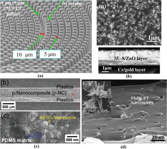
Figure 9. Examples of piezocomposites: (a) SEM image of PMN–PT pillars fabricated by reactive ion etching before the epoxy filling for (1–3) piezocomposite fabrication. Reprinted from [60] with permission © 2012 Elsevier. (b) SEM images of SU-8/ZnO nanocomposite: the surface morphology of the composite (top) and a cross section of the composite layer on top of the Cr/Au electrode (bottom). Reprinted with permission from [56] © 2013 Elsevier. (c) SEM images of the BaTiO3 NP/MW-CNT/PDMS composite: a cross section of the composite with top and bottom plastic layers with evaporated electrodes (top) and close-up image showing the different elements of the composite (bottom) © 2012 Wiley-VCH Verlag GmbH & Co. KGaA, Weinheim, reprinted with permission from [28]. (d) SEM Image of the PMN–PT nanowire based/PDMS composite and the inset shows an individual nanowire based PMN–PT particle, reprinted with permission from [57] © 2013 American Chemical Society.
Download figure:
Standard image High-resolution image4.2.2. (0–3) piezocomposites
The preparation of piezocomposites with (0–3) connectivity is simpler than that of (1–3), as it is a simple process of mixing the inorganic material particles with the polymer before the latter is cured. Such composites are easier to be integrated in microscale devices for MEMS applications than the (1–3) composites, so long as the size of the particles embedded is reasonably smaller. Modeling of such fabricated composites is more difficult than (1–3) composites. This is because of the practical limitation of the (3–3) connection possibility in fabrication and also the complexity introduced if more than one type of particles are used.
Recent research has been done to incorporate ZnO nanoparticles in SU-8 for piezoelectric applications, shown in figure 9(b), [75]. Although ZnO has a small coupling coefficient, the significance of such a composite lies in the selection of the SU-8 polymer. SU-8 is a UV negative photopatternable polymer which has been utilized in different polymer MEMS applications [76, 77]. Therefore, direct UV patterning of the spin coated composite simplifies the fabrication of MEMS devices. ZnO nanoparticles of diameter less than 100 nm were used to fill dissolved SU-8 with different concentrations. ZnO nanoparticles should not exceed 20% weight filling of SU-8 in order to achieve good patternability of SU-8 [78]. For patterning a 1.5 μm thickness, the exposure dose for 20% weight ZnO/SU-8 was reported to be 6 times larger than that of pure SU-8. The use of the material has recently been demonstrated for an energy harvesting application [56].
Other composites using PDMS as the polymer have been developed. For example, 12 wt% barium titanate BaTiO3 nanoparticles of ≤100 nm diameter and 1 wt% multi-walled carbon nanotubes MW-CNT of 5–20 nm diameter and ∼10 μm length were mixed with Sylgard 184 PDMS precursors before curing. SEM images of the developed composite are shown in figure 9(c). The addition of the MW-CNT enhances the orientation of the nanoparticles during the poling process and consequently the piezoresponse. Films of up to 13 cm width and 300 μm thickness were fabricated and used for energy harvesting [28]. In another recently developed composite, PMN–PT single crystal nanowire based particles were mixed with PDMS with 10 wt% ratio. The innovation in this recent study is mainly in the chemical synthesis of the PMN–PT particles. Figure 9(d) shows a SEM image of the composite. The inset of the image shows an individual nanowire based particle where different nanowires of 200–800 nm diameters form the particle of ∼10 μm maximum width. To sum up, these different examples of (0–3) composites using nanoparticles are easier and cheaper to fabricate than the (1–3) composites with smaller scale devices, keeping the high performance piezoelectric response of the nanoparticles and the mechanical flexibility of polymers.
4.3. Voided charged polymers
There are many examples in the literature that are based on the concept of voided charged polymers. Different representative examples were selected based on the fabrication. The first category of VCPs is manufactured based on void formation and an expansion process. The second category is based on bonding different layers of the same material or of different materials in a way to introduce voids in between the layers. The first two categories produce the VCP films separately, not being integrated with any other material or structure. The third category is unique on its own as the fabricated cellular Parylene structure is the only micromachined VCP reported in the literature that is integrated on a silicon substrate. Table 4 summarizes the key features of the different VCPs reported in the recent five years.
Table 4. State-of-the-art voided charged polymers.
| Material | Film dimensions | Quasistatic d33 | Poling process |
|---|---|---|---|
| Void formation and expansion based VCPs | |||
| Cellular polypropylene [79, 80] | 85 μm thick sheets | d33, f = ∼200 pC N−1 at room temperature | N/A |
| Fluorinated and post-treated cellular PP [81] | 50 μm thick sheets with 40% voids | After 9 days | Corona poling |
| d33, f = ∼270 pC N−1 at 70 °C | • Tip voltage: 25 kV | ||
| d33, f = ∼200 pC N−1 at 90 °C | • Temperature: RT for 30 s | ||
| • Gas: nitrogen | |||
| COC based cellular electrets [82] | — | After 9 days | Corona poling |
| d33, f =∼13pC N−1 at 110 °C | • Tip voltage: 60 kV | ||
| • Temperature: RT for 60 s | |||
| • Gas: N2 or SF6 | |||
| Cellular polyethylene-naphthalate (PEN) [83] | 60 μm thick sheets with 30% voids | d33, f = ∼45 pC N−1 at RT d33, f = ∼30 pC N−1 at 100 °C | DC electrode poling • DC voltage: 8.5 kV • Temperature: RT for 30 s • Gas: ambient air |
| Multilayer VCPs | |||
| PTFE/FEP multilayer VCP [84] | 5 layers of 150 μm total thickness with 40% voids | d33, f = ∼225 pC N−1 at 90 °C | Corona poling |
| • Tip voltage: 20 kV | |||
| • Temperature: RT for 20 s | |||
| FEP multilayer [85] | 2 layers of 85 μm total thickness with 80% voids | d33, f = ∼1000 pC N−1 at 120 °C after two days | Triangular electrode poling |
| • Electric field: 18 MV m−1 @ 50 Hz | |||
| • Temperature: RT | |||
| Cellular PDMS [86] | 3 layers of 300 μm total thickness with 25% voids | d33, f = 1148 pC N−1 at RT | Triangular electrode poling |
| • Electric field: 35 MV m−1 @ 0.2 Hz | |||
| • Temperature: 90 °C | |||
| Micromachined integrated cellular Parylene [87, 88] | 10 × 18 voided cell structure: each cell has the dimensions 820 μm × 80 μm and the depth is 350 μm | d33, f = 1200 pC N−1 at RT stable after 120 days | Soft x-ray charging |
4.3.1. Void formation and expansion based VCPs
This category of VCP is the first type developed and the most characterized from a material analysis perspective. The pre-poling fabrication is based on two steps. The first one is the formation of air voids inside the polymeric film. The second step is to resize the voids to allow higher charge density on the surfaces and consequently higher piezoelectric response. The resultant fabricated film is usually in the range of 80–100 μm thick, as indicated from table 4. Cellular polypropylene (PP) is the most popular of this type of VCP and actually the first material that was synthesized as a space charged electret in 1987 [89]. It is still the most cited and used VCP material for acoustic applications and electromechanical transduction.
Figure 10 shows the process steps to fabricate the cellular polypropylene, as explained in different references [31, 32, 90]. Briefly, the synthesis of cellular PP involves the following steps: (a) generation of the voids through introducing microscale particles inside PP and stretching (see figures 11(a)), (b) adjustment of the voids' size through applied gas pressure and heating cycles (see figures 11(b)) and (c) generation of the dipoles through electrode or corona poling. The resultant cellular PP has 'lens-like' shaped voids which are anisotropic and with crystallinity <50% [31]. This anisotropy makes the film more flexible across the thickness than laterally. Another method has been developed [83] in which the voids are formed by diffusion of supercritical CO2 inside the polymer film (polyethylene-naphthalate PEN in this case) followed by heating to expand the gas inside the film and form the voids. Although the quasistatic d33 in this case is lower than that of cellular PP, however, it showed more thermal stability at high temperature.
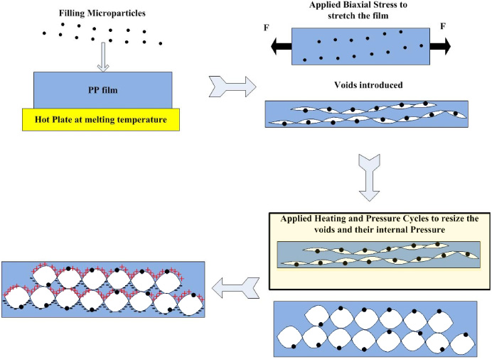
Figure 10. The fabrication process for cellular polypropylene.
Download figure:
Standard image High-resolution image
Figure 11. Cellular polypropylene: (a) after the void generation and (b) after the void size adjustment © 2004 IEEE. Reprinted with permission from [90].
Download figure:
Standard image High-resolution imageGiven the complexity of the piezoelectric response of such a material as explained in section 3.3.1, the characterization of cellular PP was mainly through experimental testing [29, 91]. Nevertheless, a recent study has proposed a finite element model to analyze and predict the piezoelectric coefficient for a cellular PP at different conditions [92]. The reported quasistatic piezoelectric d33 coefficient ranges in the literature from 150–600 pC N−1 [29, 91]. This large variation is due to different conditions such as the starting film thickness and the background pressure, in addition to the factors explained in section 3.3.1.
4.3.2. Multilayer based VCP
The second way to fabricate VCP is to bond multiple layers with different porous surfaces, which introduces the voids in between the layers. This could be through bonding layers of different materials and different properties like porous polytetrafluoroethylene (PTFE) (Teflon®) and nonporous fluoroethylenepropylene (FEP) [84, 93]. Figure 12(b) shows a SEM image of two porous PTFE and three nonporous FEP layers. Similar to void formation and expansion VCPs, the shape and distribution of voids is random in this case.
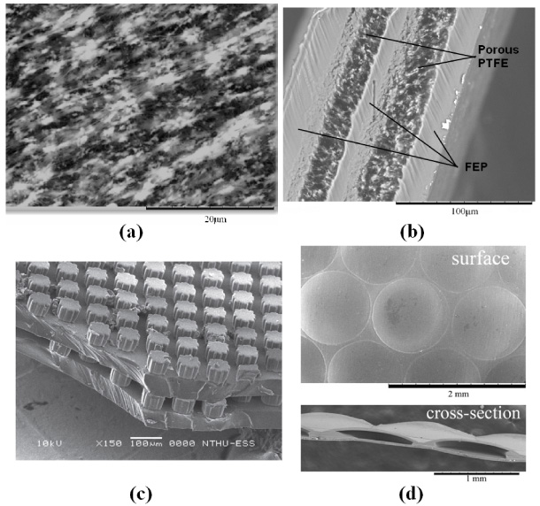
Figure 12. Multilayer based voided charged polymers: (a) porous PTFE with 91% air voids, (b) laminated PTFE and FEP layers (edited) © 2010 IEEE. Reprinted with permission from [84], (c) multilayer PDMS VCP fabricated by replica molding © 2012 IOP Publishing, reproduced by permission of IOP Publishing. All rights reserved [94] and (d) FEP VCP with hemispherical voids fabricated by pressure and thermal deformation reprinted with kind permission from Springer Science + Business Media: [85].
Download figure:
Standard image High-resolution imageAnother fabrication method for multilayer VCP is to bond layers of regularly patterned voids and in this case layers are usually of the same material. The regular patterned voids could be fabricated with different soft lithography techniques. Figure 12(c) shows PDMS VCP fabricated by replica molding of the PDMS pillars from an SU-8 on silicon mold and layer bonding via oxygen plasma surface activation [94]. The other example shown in figure 12(d) is FEP bonded layers with hemispherical air voids fabricated by pressure and thermal deformation on a metal template [85]. A good review of the different non-conventional polymer patterning methods can be found in [6] for interested readers. Regular void arrangement allows better modeling and design. In this case simplified analytical models can predict the behavior of such VCP [95].
4.3.3. Micromachined cellular Parylene
Micromachined cellular Parylene VCP is a unique example by itself that we chose to discuss as a different category from the previously mentioned two types of voided charged polymers. This is because of its unique fabrication as well as the poling process. The cellular Parylene is fabricated by vapor deposition of Parylene on a silicon mold micromachined by reactive ion etching. The silicon is then etched to release the Parylene structure that is clamped to the silicon wafer. Figures 13(a) and (b) show SEM images of the released Parylene clamped structure. This structure is charged with the distinctive soft x-ray setup [87] shown in figure 13(c). Soft x-ray tubes are usually used as a tool for charge neutralization of surfaces. Here, a high bias voltage across the VCP is applied so that the photo-ionized gas molecules, by the soft x-rays, are selectively implanted on opposite surfaces of the cellular Parylene structure to form the macro-dipoles of the VCP. This structure opens up the possibilities for on-chip integration of VCP with silicon electronics, a unique feature that has always been considered a challenge for VCP.
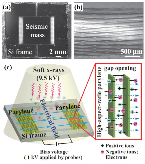
Figure 13. Integrated cellular Parylene device: (a) overall device with cellular Parylene structure suspending the seismic mass, (b) close-up image showing the clamped freestanding cellular Parylene structure and (c) a schematic diagram of the soft x-ray based charging process. Reprinted with permission from [87] © 2012 American Institute of Physics.
Download figure:
Standard image High-resolution image4.3.4. General remarks on voided charged polymers
The piezoelectric response of VCP is very attractive given the simplicity of the structure and the value of polarization per applied stress obtained. On-chip integration is limited to only the micromachined Parylene electret discussed in the previous section. All other VCP are sheets in the thickness range of 50–300 μm, which are useful in applications that would require a membrane electromechanical structure, commonly used in acoustics and ultrasonics. Another important challenge is the lifetime of the trapped charges in the VCP and the thermal stability of the structure for high temperature operation. Although it is rarely discussed in the literature, there are two trends for increasing the thermal stability of the VCP. The first approach is the fabrication of VCP based on thermally stable dielectric materials, mainly fluorocarbon based polymers like FEP and PTFE. This can be seen from the examples in table 4, where fluorine based polymers show higher stability of piezoelectric response up to 120 °C. Also, in the micromachined Parylene electret, the fluorine-containing Parylene dix-F was used as the initial coating to enhance higher thermally stable charge density on the surface [88]. The other approach is to chemically modify the surface properties of polymer materials to maintain the charges at high temperature. For example, the surface of PP was modified by polyhedral oligomeric silsesquioxane (POSS) to reach thermally stable operation (120 pC N−1) up to 85 °C [96]. In the cellular PDMS multilayer based VCP, the surfaces were coated with PTFE using a chemical wet process [94]. With regards to the lifetime and aging effects, if used at room temperature the space charges can maintain its density on the VCP for years, which is why the electret microphone has become a successful product since its invention [32]. However, the longest period of aging study at higher temperature (more than 80 °C) found was 20 days [96], which is still a short term period for an industrially useful application. Despite all these challenges, VCPs inspire more creative solutions and studies to reach a long term stable application at high temperature.
5. Comparative analysis of piezoelectric polymers
As conveyed by the review above, there is a large range of polymers and polymeric structures that are piezoelectrically responsive. However, when it comes to actual applications, there are certain concerns and factors that should be considered for choosing a certain type over another, the most important of which can be listed as follows:
- (1)The minimum response required for the application: this is directly related to the coupling coefficient of the material: the higher the coupling coefficient kii, the higher the response. For an effective coupling efficiency, the dielectric loss tanδe and the mechanical loss tanδm should also be considered, as they degrade the ratio of the generated energy to the energy applied. In this case, a sufficient figure of merit for the piezoresponse can be considered as

- (2)Lifetime of the application: there are certain applications that require operation at elevated temperatures for a long time. Such applications need a piezoelectric material not only with a high 'Curie' temperature but also with less aging effects.
- (3)The level of integration required: the previous two criteria are related to the material properties whereas this criterion adds another important factor for the selection, which is related to the flexibility of fabrication processes related to each material. Integrating a system on chip mostly requires the ability to process thin films while thick films with large feature size can be integrated off chip.

In the remainder of this section, we will focus on the first two factors to compare the material properties of the different piezoelectric polymers. The level of integration will be addressed as part of the applications section discussed later. For a broader picture, the analysis includes the three most common inorganic piezoelectric materials which are PZT, AlN, ZnO and the recently developed PMN–PT material. Some important properties of these materials are shown in table 5.
Combining factors (1) and (2) mentioned above, characteristic figures have been generated to compare the different materials. Attention is directed to the 33 mode coupling because it is always higher than the 31 mode, in addition to the fact that it is available and cited for the materials under discussion. Also, it should be noted that the k33 value used for the comparison has been calculated at room temperature for all materials.
Table 5. Material properties of inorganic piezoelectric materials under consideration.
| PZT PIC 151 [97] | AlN [13] | ZnO [98] | PMN-0.29PT [66] | ||
|---|---|---|---|---|---|
| Density | (kg m−3) | 7800 | 3230 | 5610 | 8000 |
| Young's modulus Y | (GPa) | 60 | 308 | 201 | |
| Dielectric constant εr | εr33 | 2400 | 10.5 | 11 | 5500 |
| εr11 | 1980 | 10.5 | 8.5 | ||
| Dielectric loss tanδe | 0.02 | 0.005 | 0.05 | ||
| Mechanical loss tanδm | 0.01 | 0.01 | 0.01 | 0.01 | |
| d33 | (pC N−1) | 500 | 5.5 | 12.4 | 2000 |
| d31 | (pC N−1) | 210 | 1.73 | 5 | |
| k33 | 0.69 | 0.31 | 0.48 | 0.9 | |
| k31 | 0.38 | 0.1 | 0.18 | ||
| Maximum use temperature | (°C) | 250 | 1150 | 750 | ∼130 [99] |
Figure 14 shows the coupling coefficient k33 plotted against the maximum operating temperature for the polymeric and inorganic piezoelectric materials while figure 15 plots the figure of merit for these materials where data is available. The piezocomposites and the VCPs were excluded from the figure of merit due to the difficulty in estimating the dielectric and mechanical losses from the literature. Actual measurement of the two quantities is required. From the two figures, we can conclude the following:
- (1)By assessing the piezoelectric properties of the bulk piezoelectric polymers, PI (β-CN)APB/ODPA can be considered the best choice. First, it has the highest operating temperature for all polymers. Second, although it has a much lower coupling coefficient, k33, than the PVDF family (see figure 14), its smaller dielectric loss makes its FOM in the same range as that of PVDF.
- (2)The piezocomposites take the advantages of both inorganic piezoelectric materials and polymers. This is clear from their intermediate values of the coupling coefficients k33 compared with piezoelectric materials and inorganic materials. The best performance is of the PMN–PT composite, which outperforms the other inorganic materials, rather than PMN–PT. The maximum operating temperature is limited by the glass transition temperature of the epoxy used. The low modulus of piezocomposites is a big advantage over inorganic materials in some sensing and energy harvesting applications.
- (3)Although the quasistatic piezoelectric coefficient of the VCPs is the highest compared to all piezoelectric materials, the effective low Young's modulus in the direction of the piezoelectric response leads to a low value of the coupling coefficient. This can be seen from the selected VCPs plotted in figure 14.
- (4)The dielectric loss plays an important role in characterizing the piezoelectric response, even between the inorganic materials. This can be seen in the FOM of AlN.

Figure 14. Coupling coefficient k33 versus maximum operating temperature.
Download figure:
Standard image High-resolution image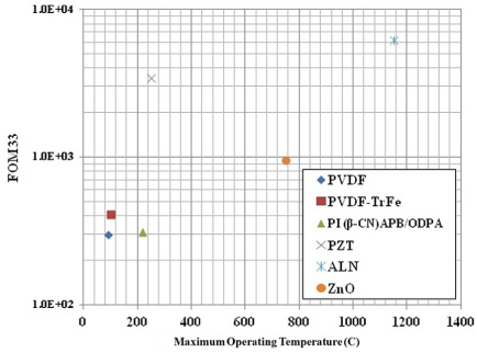
Figure 15. Piezoelectric coupling figure of merit versus maximum operating temperature.
Download figure:
Standard image High-resolution image6. Applications of piezoelectric polymers
6.1. Piezoelectric tactile sensors
A tactile sensor is defined as a device that can measure a physical phenomenon through contact and touch [100]. This measured phenomenon could be temperature, shape, softness, pressure or force [100]. This type of sensor has potential uses in robotics as well as medicine [101]. Piezoelectric polymers are relevant for such applications in measuring force or pressure. It should also be noted that the pyroelectricity of the ferroelectric polymers can be used to measure tactile temperature. This introduces complexity for reliable measurement of each phenomenon without crosstalk. As mentioned in section 4.1.1, selective poling of ceramic/PVDF composites can enhance piezoelectricity over pyroelectricity or vice versa and this allows the integration of force and temperature tactile sensors without cross talk [40]. Despite the high sensitivity of piezoelectric tactile sensors, their use is limited to sense dynamic forces and pressures only, as the charge generated due to a static stress of the piezoelectric material dissipates, depending on the dielectric constant and the resistivity of the material [4, 100].
Table 6. Summary of piezoelectric based tactile sensors.
| Material | Sensitivity | Spatial resolution | Comments |
|---|---|---|---|
| PVDF–TrFE [19] | 9.1–10.6 mV N−1 | 1.5 mm × 1.5 mm | Sensitivity changes with the shape and dimensions |
| PVDF–TrFE [35] | 0.35–0.7 μV Pa−1 | 1.5 cm × 1.5 mm | Sensitivity changes based on PVDF–TrFE layer thickness |
| PVDF [51] | 42 mV N−1 | 4.4 mm × 4.4 mm | Electrospun fibers between metal electrodes |
| PVDF–TrFE [53] | 50 mV N−1 | 1 mm × 1 mm | Polymer layer integrated on top of the gate of a CMOS transistor |
| PVDF–TrFE PZT composite [40] | 7.3 nA/bar | 10 mm × 10 mm | The piezoelectric element is connected to the gate of an organic thin film transistor (OTFT) and the sensitivity is modulated by the current change in the OTFT |
| Cellular PP [102] | N/A | 5 mm × 5 mm | The application is a touchpad where the purpose is to allocate the location of the touch on the cellular PP film by comparing four different signals |
Figure 16 shows different examples of tactile sensors based on flexible piezopolymers. Piezoelectric tactile sensing is a unique piezoelectricity application that necessitates the use of polymers over the inorganic materials due to the mechanical flexibility and softness that is needed for the application. Even when an inorganic piezoelectric material is used in such an application, it is either in the form of an inorganic/polymer composite [40] or a thin film deposited on top of a flexible substrate [103, 104]. As can be seen from table 6, PVDF–TrFE is the material of choice for such an application. This is because of its biocompatibility and being the most commonly used polymer due to its highest k33. Generally, the design of a tactile sensor is basically a two-plate capacitor with the piezoelectric polymer as the dielectric material, where the applied force induces a charge across the capacitor which is sensed by a voltage or charge amplifier circuit [4]. Such an approach is not suitable for a high density array of sensors which is a requirement of effective tactile sensing. There is another design approach that can allow the high density array of sensors, which is the fabrication of the piezoelectric polymer film on top of the gate of a transistor. The piezoelectric signal changes the gate voltage modulating the drain source current. The largest density experimentally characterized in the present devices is the 5 × 5 array of the piezoelectric oxide semiconductor field effect transistor (POSFET) shown in figure 16(a) [53]. The high sensitivity and the smallest spatial resolution make the POSFET tactile sensor the best choice for robotics applications. However, a big limitation of the device presented is that it is still fabricated on a rigid silicon substrate. That's why designs of the same idea are fabricated with organic thin film transistors on a polymer substrate but with less sensitivity and spatial resolution [40, 55]. To keep the high performance of the CMOS based tactile sensor, a novel process of flexible single crystal silicon developed by Rojas et al [105] can be used to release high performance POSFETs for tactile sensing.
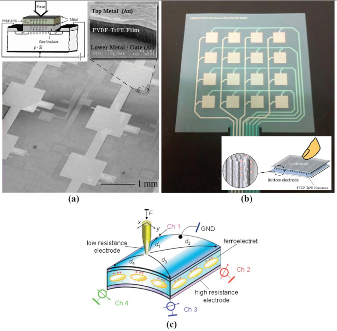
Figure 16. Examples of tactile sensors: (a) POSFET sensors: SEM image showing part of the 5 × 5 array of sensors. The top left inset shows a schematic of the sensor and the top right inset shows the cross section of the PVDF–TrFE film © 2011 IEEE. Reprinted, with permission, from [53]. (b) Sub-20 nm PVDF–TrFE nanograss based tactile sensor. Inset shows an illustrative schematic of the sensor © 2012 IEEE. Reprinted, with permission, from [48]. (c) Cellular PP based touchpad. Reprinted with permission from [102] © 2008 American Institute of Physics.
Download figure:
Standard image High-resolution imageFigure 16(b) shows a tactile sensor array based on the PVDF sub-20 nm nanograss mentioned in section 4.1.1. The nanograss PVDF sensor showed a sensitivity of 0.56 V when hit with a 98 mN force, a response 2.8 times higher than regular flat thin films [48]. Other researchers implemented a tactile sensing array using only polymer materials by inkjet or screen printing [55]. Cellular PP has also been utilized in a touchpad large area sensor (see figure 16(c)) which is based on signal analysis of four different voltage signals at the corners of a cellular PP film to identify the touch location. These several examples show the significance of flexible piezopolymers for tactile sensing applications.
6.2. Vibration energy harvesters
Energy harvesting from vibration continues to be an active field of research with the ambition that such harvesters could replace batteries or increase their lifetime [106]. There are many novel designs based on piezoelectric materials that are reviewed in different references [38, 106–109]. A good design of vibration energy harvester is dependent on the highest harvested power possible with the smallest area at the optimal frequency of the vibration source harvested [107]. Such an application requires the highest coupling coefficient k for maximum power conversion. From the comparison presented in section 5, the inorganic materials are much more effective. However, the advantage of using polymers over ceramics comes back to the mechanical flexibility and lower stiffness of the piezopolymers. This flexibility prevents fatigue and increases the lifetime of the device, especially in low frequency vibration or applied impact force [106]. This advantage is not only for the active piezoelectric material but also for the electrode materials. For example, a study showed that the use of conductive polymer PEDOT/PSS for the electrodes with PVDF harvesting devices shows more robustness than Pt or ITO electrodes which were damaged after operation at frequencies higher than 33 kHz and 213 Hz, respectively [110].
To compensate between high coupling and flexibility, the choice of polymer composites is optimal. This is what Patel et al [111] suggested as (1–3) PZT/Epoxy composite harvesters generated the highest output voltage when compared with PVDF and cellular PP. Also, MFC® has been utilized in a cantilever based energy harvester which could generate 151.6 μW at a resonant frequency of 20.6 Hz [68]. Cantilevers fabricated with SU-8/ZnO nanocomposite (see figure 17(a)) generated 0.025 μW at 4 kHz frequency when connected to 100 kΩ load [56]. To harvest more energy, researchers proposed another design approach where the high power generation is adjusted to a broad band of frequencies rather than a single resonant frequency. For example, Jo et aldesigned a novel PVDF based energy harvester with a tunable resonant frequency broadening the frequency band of harvested vibration by automatically changing the suspension beam lengths with the applied frequency, as shown in figure 17(b) [44]. Another design based on MFC® integrated with magnetic oscillation allowed a broader band of low frequency vibration [112].

Figure 17. Examples of piezopolymer energy harvesters: (a) SU-8/ZnO nanocomposite cantilever: schematic with layer dimensions (left) and SEM image (right). Reprinted with permission from [56] © 2013 Elsevier. (b) Schematic illustration of PVDF based frequency tunable energy harvester (edited) © 2012 IOP Publishing, reproduced by permission of IOP Publishing. All rights reserved. (c) Experimental illustration of using the BaTiO3 NP/MW-CNT/PDMS composite in power generation from human motion © 2012 Wiley-VCH Verlag GmbH & Co. KGaA, Weinheim, reprinted with permission from [28].
Download figure:
Standard image High-resolution image
The vibration source could be also in the form of mechanical taping at a very low frequency in the range of less than 10 Hz. Such mechanical force can be found in human motion, an inspiration for 'self-powered wearable devices' [113]. For such applications, the BaTiO3 NP/MW-CNT/PDMS based 4 cm × 4 cm sheet, shown in figure 9(c) top, was used to generate an open circuit voltage of ∼3.2 V and short circuit current of 250–350 nA under periodic mechanical tapping [28]. Figure 17(c) shows another sheet of the same composite under mechanical tapping with a human leg to simulate the power generation from walking. The PMN–PT nanowire based/PDMS composite generator, shown in figure 9(d), produced a maximum voltage of 7.8 V and maximum short circuit current of 2.29 μA under periodic mechanical tapping of a 1 cm × 0.5 cm sheet [57]. In brief, piezoelectric polymers, especially composites, are favorable for low frequency vibration energy harvesting, especially when it comes to flexibility and reliability.
6.2.1. Vibration energy harvesting and impedance matching
Another point of consideration in assessing the performance of vibration energy harvesters is the matching between the harvester input impedance and the output load impedance [114]. The output load impedance for most of the low power applications (10 Ω to a few kΩ range) is found to be much lower than the harvester input impedance (hundreds of kΩ to MΩ range) [109]. It is found that this point is usually neglected among the MEMS designers of energy harvesters, and output power is reported at the optimal output load, or the output open circuit voltage is reported. That's why in most of the literature the impedance matching problem is tackled by developing interface circuits to match the input and output impedance rather than optimizing the impedance electromechanical transducer that harvests the energy [114]. The impedance of the energy harvester is inversely proportional to its capacitance, i.e. the dielectric constant of the piezoelectric material. Comparing materials in section 5, the dielectric constants of inorganic materials are higher than that of piezoelectric polymers. This suggests the same point about the use of piezocomposites as the material of choice for energy harvesting. Regardless of the piezoelectric material used, there is a MEMS design approach that is used to overcome the high impedance problem which is the use of multilayer structures [115, 116]. The use of multilayer structures stacked with alternating polarization direction reduces the device impedance and increases the current output [115, 116]. The mechanical flexibility of the piezoelectric polymers in addition to the multilayer design approach has the potential for optimal power generation at low impedances, as theoretically illustrated by Zhang et al [115].
6.3. Acoustic transducers
Acoustic transducers are vibration based electromechanical transducers that operate in the acoustic spectrum range including audio, ultrasonic and infrasonic frequency ranges [117]. The piezopolymer based acoustic transducers include microphones [50], loudspeakers [82] and ultrasonic transducers [67, 79, 118]. Table 7 reports different acoustic devices based on piezoelectric polymers. The reported MEMS microphone sensitivity is defined as the voltage variation per applied sound pressure on the Parylene-C [50]. For a loudspeaker, the figure of merit is the sound pressure level (SPL) which is defined as the effective pressure of sound relative to a reference ambient pressure [50]. The SPL changes with frequency in loudspeakers. Acoustic emission sensors (AES) are electromechanical sensors that passively detect the acoustic signal due to a mechanical or shape change in the system it is used in. The main difference between AES and an ultrasonic transducer is that it detects the acoustic signal passively while an ultrasonic transducer transmits a signal and receives the reflected signal to detect any change. AES are usually implemented in applications where continuous monitoring is needed, such as material fracture or device failure. On the other hand, ultrasonic transducers are used in other applications such as medical imaging and automated machinery [119]. There are many examples of ultrasonic transducers in the literature and we reference here the main ones that were designed recently [59, 60, 66, 72, 74, 80, 118, 120]. We chose to list in the table two studies that have used different materials to reach the same optimum frequency to indicate the difference in performance between the different composite materials.
Table 7. Acoustic device based piezoelectric polymers.
| Material | Application | Figure of merit | Design and size |
|---|---|---|---|
| Parylene-C [50] | MEMS microphone | Average sensitivity 5.5 μV Pa−1 up to 10 kHz | A 6 mm Parylene-C membrane fabricated on a silicon wafer |
| COP voided charged polymer [82] | Loudspeaker | SPL 10–60 dB for frequency 1–10 kHz | 8 bonded layers of COP VCP layers (15 cm × 15 cm) area |
| COC voided charged polymer [121] | Loudspeaker | SPL 60–80 dB for frequency 1–10 kHz | 5 bonded layers of different patterns with total size 120 mm × 120 mm × 70 μm |
| PVDF [122] | Acoustic emission sensor for drilling process monitoring | Variation in sensed voltage during different process steps depending on material drilled | Hot embossed PVDF multilayers with an epoxy detection head fabricated by replica molding assembled in an cylindrical packaging of 16 mm diameter and 12 mm height |
| MFC® [67] | Acoustic emission sensor for detection of damage location | Location detection with average STD 12.5–70 mm depending on the material | MFC® rosettes with each (25 mm × 12 mm) placed in material plates of dimensions at least (12''× 12'') |
| PVDF [118] | 25 MHz ultrasonic transducer | −6 dB bandwidth = 108% Insertion loss = −39.5 dB | Circular membrane with diameter/thickness 1.8 mm/28 μm within optimized matching layers |
| (1–3) PZT/epoxy composite [118] | 25 MHz ultrasonic transducer | −6 dB bandwidth = 118% Insertion loss = −34 dB | Circular membrane with diameter/thickness 3 mm/50 μm within optimized matching layers |
| (1–3) PMN–PT/Epoxy composite [66] | 2.5 MHz ultrasonic transducer | −6 dB bandwidth = 94.5% Insertion loss = −21.3 dB | Angle beam two element transducer with composite sheets of dimensions22 mm × 13 mm × 0.60 mm |
| (1–3) PZT/epoxy composite [66] | 2.5 MHz ultrasonic transducer | −6 dB bandwidth = 72% Insertion loss = −27.3 dB | Commercially available (1–3) PZT transducer from (CCN-DT) |
| Cellular PP [80] | Air-coupled ultrasonic transducer | Power transmission coefficient PTC = 300 × 10−12 for actuation voltage of 3000 V | Two clamped PP films, one acting as ultrasonic transmitters and receivers coupled through air PTC = Power received/power transmitted |
6.4. Inertial sensors
Inertial sensors are electromechanical sensors that detect velocity, acceleration or orientation [4]. This includes two main MEMS devices: accelerometers for acceleration measurement and gyroscopes for orientation. Table 8 summarizes the piezopolymer based inertial sensors found in the literature which are mainly accelerometers. The main criteria for comparing accelerometers are the sensitivity, frequency range, acceleration range and the total area and volume of the device. These parameters are compared along with the design principle. As can be seen from the size values, piezopolymer accelerometers are in the scale of mm, not in the scale of micrometers. They are also fabricated off chip and not integrated with circuitry, a main drawback of these accelerometers, especially if compared with capacitive silicon micromachined accelerometers [123], which are smaller in size with a broader working range. Yet, the advantage of piezoelectric accelerometers is that they don't consume power to operate, which is not the case in capacitive accelerometers.
Table 8. Accelerometer sensors based on piezoelectric polymers.
| Material | Sensitivity | Working range | Design and dimensions |
|---|---|---|---|
| PVDF–TrFE [54] | • Sensitivity = 0.57 pC g−1 |
• Frequency: 0–200 Hz • Acceleration: 0–7 g | • PVDF–TrFE (0.83 mm × 1 mm × 0.2 mm) layer on top of a suspended mass system of polypropylene material with total area6 mm × 6 mm |
| Cellular PP [124] | • Variable sensitivity increases by decreasing static pressure Ps and increasing mass m | • Variable frequency increases by increasing static pressure and reducing mass • Acceleration: 0–11 m s−2 | • A mass supported by metallic springs and attached to the top of a cellular PP film fixed from the other side on a rigid plate • Mass area: 2.9 cm2 |
| FEP electret and cellular PP [125] | • Variable with the same trend as cellular PP but lower sensitivity values in general | • Variable frequency with similar trend • Acceleration: 0–6 g | • Same mass and spring (as in [124]) but attached to an FEP electret suspended by cellular PP ring acting as a moving support to the FEP membrane which is moving against a rigid stationary plate. The main charge variation is between the FEP electret and the stationary plate, not the cellular PP • Mass area: 11.5 mm, ring width: 1.5 mm |
7. Conclusion
Piezoelectric polymers are a class of functional polymers that can be utilized in different transduction applications. This paper reviewed the working principle of the different types of piezoelectric polymers classified into three categories: bulk piezopolymers, piezocomposites and voided charged polymers. Although a high electric field is required, the poling process is necessary for an efficient piezoelectric response. The state-of-the-art materials in each category have been reported with the focus on fabrication methodologies and material properties. There are a variety of fabrication methods for piezopolymers which are different from standard silicon microfabrication techniques. These fabrication methods (such as replica molding, imprinting and thermal deformation) are usually easier and less expensive than inorganic material microfabrication. A comparative study between the different piezoelectric polymers with the most common inorganic piezoelectrics has been presented. The study showed that the efficiency of transduction is highly dependent on the dielectric loss. This is what makes amorphous polyimide (β-CN)APB/ODPA with its polar nitrile group the most efficient piezoelectric bulk polymer among the studied materials. Further developments are needed to utilize this material in useful MEMS devices. The study also showed how complex it can be in comparing voided charged polymers with other piezoelectrics, which is due to the large frequency dependence of the piezoelectric coefficient and the stiffness constants of the material. The applications of the piezopolymers materials have also been reported with the key design aspects of each device and its use. Piezopolymers offer a unique choice, particularly in tactile sensing applications and some acoustic devices due to the need for mechanically flexible materials for such applications. Piezocomposites are more advantageous when it comes to choosing a piezoelectric polymer material for an energy harvesting application due to their highest coupling coefficients. The newly developed PMN–PT epoxy composites are very promising and future work will be directed to utilize such composites in microfabricated devices. Polymer based piezoelectric materials offer a huge variety of piezoelectric properties with favored mechanical flexibility and mostly easier and lower cost fabrication methods for millimeter and micrometer scale sensors and energy harvesters.
Footnotes
- a
Values calculated based on other parameters reported in the reference.
- a
Temperature is estimated based on the glass transition temperature of the polymer.
- a
g refers to the gravitational acceleration: g = 9.8 m s−2.