Abstract
In this review, we summarize solution-processed oxide thin-film transistors (TFTs) researches based on our fulfillments. We describe the fundamental studies of precursor composition effects at the beginning in order to figure out the role of each component in oxide semiconductors, and then present low temperature process for the adoption of flexible devices. Moreover, channel engineering for high performance and reliability of solution-processed oxide TFTs and various coating methods: spin-coating, inkjet printing, and gravure printing are also presented. The last topic of this review is an overview of multi-functional solution-processed oxide TFTs for various applications such as photodetector, biosensor, and memory.
Export citation and abstract BibTeX RIS
1. Introduction
Since amorphous Si thin-film transistors (TFTs) face the barrier which is limited application field due to their low electrical characteristics, many alternative materials have been researched. Among the alternatives, oxide semiconductors have been brought attention as backplane materials for the next-generation flat panel display (FPD). Since Hosono presented oxide TFTs,1,2) numerous researches have been intensively studied over a decade. Oxide TFT has many advantages: high electron mobility in amorphous phase, high transparency, low leakage current, and high adaptability to various fabrication processes.3)
Among the various process technologies, solution process has many advantages: not only simple and low cost process, but also homogeneity and excellent compositional control and high throughput. Figure 1 shows the schematic diagram of the solution process for oxide TFTs. Oxide solution was synthesized using metal precursors in solvent and deposited on a substrate by various coating methods. The coated oxide thin-film was pre-annealed to remove the solvent and post-annealed to develop an active layer. During the annealing process, there are three steps in the following order: 1) decomposition, 2) hydrolysis, and 3) dehydroxylation and alloying.
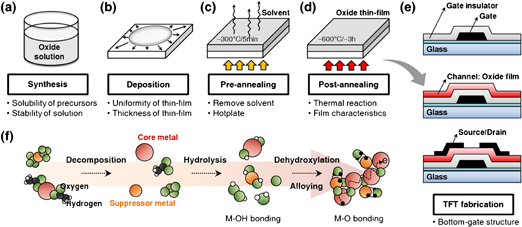
Fig. 1. Schematic diagram of the solution process for oxide TFTs: (a) Oxide solution was synthesized using metal precursors in solvent. The mixture was stirred, filtered, and then aged in ambient air. (b) The synthesized oxide solution was deposited on a substrate by various methods such as spin-coating, inkjet printing, and gravure printing. (c) The oxide thin film was pre-annealed to remove the solvent and (d) post-annealed to develop an active layer. (e) The bottom-gate top-contact TFT structure was fabricated using solution process. (f) The entire chemical reactions in the oxide solution.
Download figure:
Standard image High-resolution imageFor next-generation FPD, solution-processed oxide TFTs have been intensively investigated using InZnO (IZO),4) ZnSnO (ZTO),5,6) GaZnO,7) and InGaZnO.8) In particular, low temperature process for oxide TFTs have been recently studied in various ways using aqueous solution,9,10) deep ultraviolet (UV),11) combustion,12) and O2/O3 atmosphere annealing,13) and "sol–gel on chip".14) Moreover, solution-processed gate insulators have been also studied after ZrO,15) HfO,15) Al2O3,16,17) and Y2O317) were presented. Figure 2 summarized by surveying Google scholar from 2008 to September 2013 shows recent researches about solution-processed oxide TFTs, and the number of publications has been steadily increased. The bar chart is divided into five main categories of the oxide semiconductor: IGZO, ZnO, IZO, ZTO, and others including InO, InSnO (ITO), InSnZnO (ITZO), SnO, TiO, and CuO.

Fig. 2. Number of published papers related solution-processed oxide TFTs since 2008. In the legend, "others" includes InO, ITO, ITZO, SnO, TiO, and CuO.
Download figure:
Standard image High-resolution imageIn this paper, we endeavor to summarize solution-processed oxide TFT researches based on our previous reports. The fundamental concept and electrical analyses of the approaches: precursor composition effects, low temperature solution processing, channel engineering, various coating methods, and multi-functional solution processing are reviewed.
2. Precursor composition of oxide thin films
Although many researches have been published since 2004, the role of each component in multinary oxide TFTs and optimal composition of oxide TFTs were not clearly defined. We studied the role of each component in oxide semiconductors, and tried to produce the optimized composition for high electrical performances.
2.1. Solution-processed active layer
2.1.1. In based active layer
To investigate a role of In atom in IGZO TFTs, we experimented with varying In composition in IGZO TFTs.18) Increased In ratio was correlated with decreased electrical resistivity, because high In ratio leaded to a large number of oxygen vacancies and Zn interstitials which are the origin of electrons. The more In atoms in IGZO induced negative shift and increasing on-current (Ion) and off-current (Ioff) of transfer curve due to more electrons. Therefore, as In ratio was increased in IGZO TFTs, field-effect mobility (μFET) was increased.
For studying Ga effects in IGZO TFTs, we varied Ga ratio in IGZO TFTs.19) As the Ga/Zn ratio increased, the electron concentration decreased, while electrical resistivity was inversely increased. This is because Ga composition acted as a suppressor in IGZO thin films. Ga ions have stronger chemical bonds with oxygen than that with the Zn and In ions due to larger formation energy of oxygen vacancy. The incorporation of Ga content in the IZO played the role of effective control of carrier generation which is related to oxygen vacancies. In conclusion, the role of Ga for IZO was a carrier suppressor.
In IGZO, higher electrical conductivity came from In and Zn. To find more effective carrier suppressors, we adopted many alternative atoms to replace Ga in IGZO. In this research, we considered three perspectives: low standard electrode potential (SEP), large bandgap, and low electronegativity.
The first trial was to use Y as a carrier suppressor in IZO. We varied Y/Zn ratio in YInZnO (YIZO) TFTs.20) For the reference, we experimented with IGZO TFTs, as well. As Y composition increased, μFET decreased, because Y acted as a carrier suppressor in IZO. These changes also caused decreased Ion and Ioff in transfer curves. As a result, optimized YIZO TFTs had higher μFET than IGZO TFTs.
In terms of SEP, lower SEP atoms act as effective carrier suppressors, because SEP is a degree of metal oxidization. Since Hf (−1.70 V) has a lower SEP than Ga (−0.52 V), Hf is more effective to reduce oxygen vacancies than Ga. To study doping effect of Hf, Hf/Zn ratio was varied in HfInZnO (HIZO) TFTs.21) From transfer curves of IGZO and HIZO, Hf was found to be more effective than Ga as a carrier suppressor, because Ioff of HIZO was much lower than that of IGZO.
In addition to SEP, metal oxide bandgap was also important for carrier suppressors, because larger bandgap can drop the donor-related levels toward the deep or intrinsic level. Since Mg has low SEP (−2.37 V) and large bandgap (∼7.9 eV), we researched Mg effects on MgInZnO (MIZO) TFTs.22) For analyzing Mg effects in IZO, we investigated MIZO TFTs as a function of Mg contents. As Mg ratio was increased, optical bandgap of MIZO, which is related to activation energy for donor-related shallow defect states, was also increased. From the transfer curves of MIZO TFTs, we confirmed Mg is an excellent material for carrier suppressor.
In addition to SEP and bandgap, electronegativity was also an important factor for carrier suppressors. As the electronegativity difference between metal and oxygen atoms became larger, the oxygen vacancies were reduced. Therefore, the lower electronegativity atom, the better carrier suppressor is. Sc is also an attractive material for carrier suppressors, because it has lower SEP (−2.36), wide bandgap (∼6.3 eV), and lower electronegativity (1.3). We varied Sc ratio in ScInZnO TFTs.23) Like other carrier suppressors, Sc was acted to decrease Ion and Ioff and move transfer curve to positive direction.
La,24) Ba,25) Sr,26) and Zr27) were also studied as carrier suppressors for IZO TFTs. All these materials found to be excellent carrier suppressors in IZO. Moreover, oxygen vacancy of In based active layer was investigated to analyze O 1s peak using X-ray photoelectron spectroscopy (XPS) analysis. Usually, O 1s peak can be deconvoluted by three regions: low binding energy (metal oxide bonding, OI), medium binding energy (oxygen vacancy, OII), and high binding energy (metal hydroxide bonding, OIII). As carrier suppressor ratio was increased, the medium binding energy region out of total O 1s region which is relative amount of oxygen vacancy was also decreased.19,23,24)
Figure 3 summarizes SEP, bandgap, and electronegativity of all carrier suppressors we have studied, and electrical properties of In based TFTs are summarized in Table I. Carrier suppressors have a tendency to satisfy above conditions. Therefore, we confirmed that the materials with lower SEP, larger bandgap, and lower electronegativity than In and Zn became excellent carrier suppressors in IZO TFTs.

Fig. 3. SEP, bandgap, and electronegativity of In, Zn, Sn, and carrier suppressible atoms.
Download figure:
Standard image High-resolution imageTable I. Electrical properties of In based solution-processed oxide TFTs. These parameters were measured under optimized composition ratio.
| Channel | Gate insulator | μFET(cm2 V−1 s−1) | On/off ratio | SS(V/decade) | Ref. |
|---|---|---|---|---|---|
| GaInZnO(1 : 3 : 2) | SiNx | 0.86 | ∼106 | 0.63 | 7 |
| YInZnO(0.3 : 3 : 2) | SiNx | 1.12 | 4.61 × 10⁵ | 1.03 | 8 |
| HfInZnO(0.2 : 3 : 2) | SiO2 | 1.94 | 3.64 × 10⁶ | 0.58 | 9 |
| MgInZnO(2 : 9 : 1) | SiNx | 2.7 | 5 × 10⁸ | 0.20 | 10 |
| ScInZnO(0.7 : 3 : 2) | SiO2 | 2.06 | 8.02 × 10⁶ | 0.93 | 11 |
| LaInZnO(0.5 : 5 : 5) | SiNx | 2.64 | 1.2 × 10⁶ | 0.68 | 12 |
| BaInZnO(0.56 : 3 : 2) | SiNx | 1.43 | ∼106 | 0.94 | 13 |
| SrInZnO(1.25 : 3 : 2) | SiNx | 0.34 | 4.54 × 10⁶ | 0.61 | 14 |
| ZrInZnO(0.4 : 3 : 2) | SiO2 | 0.77 | ∼106 | 0.73 | 15 |
2.1.2. Sn based active layer
Because In is toxic and high cost, IZO based TFTs have a few disadvantages. The importance of In free oxide TFTs have been increased, and Sn based TFTs have been researched as a promising alternative. Since the electronic configuration of Sn and In is identical except 5p orbital, Sn has similar electrical properties with In. We studied doping effects of Zr,28) Mg,29) and La30) as a carrier suppressor on solution-processed ZTO based TFTs, and electrical properties were summarized in Table II. For Sn based active layer, the medium binding energy region out of total O 1s region in XPS data was also decreased, as the carrier suppressor ratio was increased.28,29) As also shown in Fig. 3, Zr, Mg, and La were satisfied three criteria, SEP, metal oxide bandgap, and electronegativity, for carrier suppressors.
Table II. Electrical properties of Sn based solution-processed oxide TFTs. These parameters were measured under optimized composition ratio.
| Channel | Gate insulator | μFET(cm2 V−1 s−1) | On/off ratio | SS(V/decade) | Ref. |
|---|---|---|---|---|---|
| ZrZnSnO(0.3 : 4 : 7) | SiO2 | 4.02 | 3.57 × 10⁶ | 0.94 | 16 |
| MgZnSnO(0.5 : 4 : 8) | SiNx | 1.00 | 3.15 × 10⁶ | 0.92 | 17 |
| LaZnSnO(0.1 : 1 : 5) | SiO2 | 0.51 | 9.47 × 10⁶ | 1.09 | 18 |
However, even if the material satisfies for three criteria as a carrier suppressor, ionic radius must be considered. In the point of ionic radius view, La could not be a proper carrier suppressor for ZTO, because La has larger ionic radius. If doped atom's ionic radius was large, it is easy to generate oxygen vacancies, because the doped atom with larger ionic radius induces the lattice expansion of ZTO. As La ratio was increased, Ioff was not decreased like other carrier suppressors. When La ratio was larger than 0.5, Ioff was remarkably increased, because oxygen vacancies were generated by structure distortion through La doping.
2.2. Solution-processed gate insulator
All solution-processed oxide TFTs, not only solution-processed semiconductor, but also solution-processed gate insulator, are necessary for flexible application or low-cost process. We studied solution-processed gate insulator using high-k material31) and high pressure annealing (HPA) process,32) and electrical properties of oxide TFTs with solution-processed gate insulator were summarized in Table III.
Table III. Electrical properties of oxide TFTs with solution-processed gate insulator.
| Channel | Gate insulator | μFET(cm2 V−1 s−1) | On/off ratio | SS(V/decade) | Ref. |
|---|---|---|---|---|---|
| InGaZnO | YHfZnO | 0.29 | ∼105 | 1.26 | 19 |
| InZnO | ZrO2 | 0.10 | 1/17 × 104 | 1.49 | 20 |
We synthesized a new oxide material, YHfZnO (YHZO), as a gate insulator in oxide TFTs.31) To evaluate gate insulator layer, a metal/insulator/metal (MIM) structure (Al/YHZO/n+ Si) was employed by capacitance–voltage (C–V) measurement. From the C–V measurement, the dielectric constant ( ) of YHZO was calculated by 16.4. Moreover, IGZO channel and YHZO gate insulator layers have the same base material which is ZnO. By doping different atoms in ZnO layer, we can fabricate both gate insulator and active layer.
We adopt HPA for depositing ZrO2 gate insulator to reduce process temperature.32) ZrO2 solution was annealed 350 °C for 30 min under 1 MPa ambient air condition. IZO solution was deposited onto ZrO2 thin films, and annealed at 250 °C for 3 h. We have three different ZrO2 thin films: annealed at 350 °C without HPA, 500 °C without HPA, and 350 °C with HPA. By HPA treatment, ZrO2 thin films became thinner and denser. HPA treated ZrO2 at 350 °C had low leakage current density (∼109 A/cm2 at 2 MV/cm) as a gate insulator, although the films were annealed at low temperature.
3. Low temperature process for solution-processed oxide TFTs
Although solution process has many advantages, solution-processed oxide TFTs have a critical weakness, which is lower device performances than vacuum-processed oxide TFTs. In order to compensate this weakness, higher annealing temperature was required. However, at higher temperature, it is impossible to use flexible substrate for solution-processed oxide TFTs. To overcome this drawback, many researchers have made efforts to lower the process temperature with maintaining its electrical performances, and we have conducted three ways to lower the temperature: dual active layer, precursor engineering, and HPA.
3.1. Dual active layer
One approach for low temperature process is to apply dual active layer (DAL) structure for solution-processed oxide TFTs33,34) and Fig. 4 shows the schematic diagram of DAL TFTs. AlInZnO/IZO (AIZO/IZO) DAL TFTs showed a suitable switching behavior and competitive device performance at 350 °C. Due to IZO front channel which has higher carrier concentration, the charge accumulation near the interface between IZO and gate insulator was maximized. Therefore, it led higher μFET in the DAL TFTs. AIZO as a back channel in DAL TFTs was employed to control threshold voltage (Vth) and to lower Ioff.
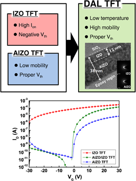
Fig. 4. Schematic diagram of dual active layer effects.
Download figure:
Standard image High-resolution imageAs the In/Zn ratio was increased in IZO layer, higher Ion and μFET were shown, whereas Ioff was also increased, and Vth was negatively shifted.33) Higher In/Zn ratio delivered higher conductivity, because oxygen vacancies were generated by additional In atoms, and In has bigger ns orbitals, which are carrier transport path. The DAL TFTs with In/Zn of 3 of IZO showed optimized switching characteristic: μFET of 1.57 cm2 V−1 s−1, on/off ratio of 1.4 × 10⁷, Vth of 1.28 V, and SS of 0.59 V/decade.
The characteristics of AIZO/IZO DAL TFTs were also modulated by varying IZO thickness and In/Zn ratio of AIZO thin-films.34) To investigate effects of IZO film thickness, we fixed In/Zn ratio of IZO layer of 3. As the thickness of IZO thin-films was increased from 8 to 12 nm, on-current was slightly increased, and the DAL TFTs with 12-nm-thick IZO thin-films showed the best transfer performances. However, the DAL TFTs with 20-nm-thick IZO thin-films showed high Ioff nearly 100 times higher than that of the DAL TFTs with 12-nm-thick IZO. These results were caused by increased carrier concentration in thicker IZO thin-films. To study In ratio in AIZO thin-films, we fixed the thickness of IZO of 12 nm, and varied In/Zn ratio 1 to 3. However, at In/Zn of 3, the increased electron flow could not be controlled because of low energy barrier of AIZO layer. Consequently, the AIZO/IZO DAL TFTs were fabricated at the temperature of 350 °C, and they showed the electrical performances (μFET of 5.62 cm2 V−1 s−1, on/off ratio of 9.0 × 10⁶, and SS of 0.53 V/decade) under optimized condition: 12-nm-thick IZO thin-films with In/Zn of 3 and AIZO with In/Zn of 1.
3.2. Precursor engineering
In solution process, it is important which precursor was used for synthesizing, because the process temperature was depending on the precursor. The proposed thermogravimetric analysis of various precursors was shown in Fig. 5. Our group investigated the precursor effect using nitrate and acetate precursor in IZO TFTs.35) IZO solution was prepared with In/Zn ratio of 3. Because In is known as poor solubility, we have used In nitrate precursor only. Zn acetate and Zn nitrate were used for Zn precursor.
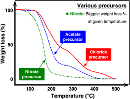
Fig. 5. Schematic diagram of thermogravimetric analyses of various precursors.
Download figure:
Standard image High-resolution imageThe IZO thin-films with Zn nitrate precursor (IZO_NP) had denser and higher carrier concentration than that with Zn acetate precursor (IZO_AP) in spite of same molarity IZO solution. As a result, the Hall mobility of IZO_NP was also higher than that of IZO_AP. To simplify precursor effect, we experimented with InO thin-films. In Fourier transform infrared spectroscopy (FT-IR) transmittance spectra of InO thin-films with In acetate precursor or In nitrate precursor, O–H stretching from 3000 to 3700 cm−1 and residual organics from 550 to 2000 cm−1 were shown in both InO thin-films until annealing temperature of 150 °C. However, the peaks of O–H stretching and residual organics in In nitrate precursor based thin-films were rapidly decreased from 300 °C, whereas the peaks of In acetate based thin-films were not decreased at 300 °C. In XPS data of C 1s data of IZO_NP and IZO_AP at 300 °C, IZO_NP had lower carbon concentration than IZO_AP. From these results, IZO_AP had poor electrical characteristics at low process temperature than IZO_NP because of high residual organic in thin-films.
While μFET of IZO_AP TFTs at 300 °C was 0.55 cm2 V−1 s−1, IZO_NP TFTs at 300 °C showed better electrical performance: μFET of 1.92 cm2 V−1 s−1. These results were caused by reducing the residual organics using nitrate precursors, so disorders in active layer of TFTs were reduced.
3.3. High pressure annealing
HPA for solution-processed oxide TFTs can change the chemical decomposition temperature, and reduce the film thickness by decreasing the porosity.36) Figure 6 shows the fabrication procedure and effect of the HPA for solution-processed oxide TFTs. Porous region which lead to unstable electrical properties for the TFTs can be decreased by HPA process. In addition, HPA can reduce the Gibbs free energy, so it can lower the fabrication temperature of solution-processed oxide TFTs.

Fig. 6. (a) High-pressure annealing procedure for solution-processed IGZO TFTs. (b) Schematic diagram of the effect of high pressure on low-temperature solution-processed IGZO thin-films.36)
Download figure:
Standard image High-resolution imageFrom C 1s data of XPS under different O2 pressures, the residual organic contents were reduced in the IZO thin-films under 1 MPa of O2 compared to non-pressurized (N/P) films. C 1s peak of the thin-films annealed under 2 MPa of O2 was similar to that of 1 MPa O2 pressurized thin-films, but 4 MPa O2 pressurized thin-films had residual organic contents as much as N/P films. The variation of organic residues under different O2 pressure was also confirmed by time-of-flight secondary ion mass spectrometry. O 1s data of XPS under different O2 pressures were also investigated. The low binding energy peak located at 529.3 eV represents oxygen ions bonding with In and Zn atoms. The medium binding energy peak located at 531.0 eV represents oxygen vacancy region, and the high binding energy peak located at 531.9 eV represents hydroxide groups (M–OH). XPS spectrum of N/P IZO films showed 13.3% of M–OH bonds, which is much larger than that of O2 HPA (5.1% for 1 MPa, 6.4% for 2 MPa, and 9.1% for 4 MPa). It means HPA can decrease the activation energy for the decomposition and oxide formation of metal-salt precursor systems. Therefore, HPA can reduce the carbon-containing residues in films effectively in spite of low process temperature. The 1 MPa O2 pressurized IZO films had the high oxide lattice content and the low residual carbon content; it affects the enhanced TFT performance than N2 and Air ambient.
1 MPa was the optimized pressure with O2 ambient in terms of electrical properties. Proper pressurizing attributed to improved bulk densification and reduced interface roughness between the channel and gate insulator, and it can help to decrease the decomposition temperature of metal-salt precursors. However, high pressure, over 1 MPa, may promote unexpected carbon- and hydrogen-containing reactions, and that arises in increased organic residues. In addition, 1 MPa O2 pressurized IZO TFTs showed smaller Vth shift under stress condition than N/P, 0.1 MPa, and 2 MPa O2 pressurized ones because of low organic residue, dense thin-films, and better interface between the channel and gate insulator. Moreover, 1 MPa O2 HPA-IZO TFTs fabricated on flexible substrate at 220 °C performed well with a μFET of 1.78 cm2 V−1 s−1, turn-on voltage of 1.12 V on/off ratio of 6.6 × 10⁶, and SS of 0.56 V/decade.
4. Channel engineering for high performance and reliable solution-processed oxide TFTs
Compared to vacuum-processed oxide TFTs, solution-processed oxide TFTs have inferior electrical properties and reliabilities due to an inherent limitation of solution-processed thin-films, i.e., low film density because of porosities such as pores and pin-holes created by solvent volatilization.
To improve the performance of solution-processed oxide TFTs, we have proposed the multistacked active layers (MSALs) which had lower porosity and higher density than the single active layer (SAL).37) Moreover, experiments were performed to assign the passivation function to the back-channel layer of the MSALs, to improve the reliability of solution-processed oxide TFTs.37–39)
4.1. Homo-stacked active layer: IGZO TFT
Generally, Vth of the vacuum-processed oxide TFTs showed a continuous negative shift with increasing active layer thickness because the carrier accumulation in the channel region strengthened due to the larger volume of the active layer. However, this phenomenon was not shown for the solution-processed oxide TFTs, which could be explained by the increased defect density due to the deterioration of film porosity. Moreover, these defects also caused inferior electrical properties and reliabilities.
Thus, to obtain enhanced electrical properties and reliabilities of solution-processed oxide TFTs, a thick active layer was fabricated by a low-molarity IGZO solution; spin-coating and pre- and post-annealing were repeated as many times as the number of layers of MSALs. The MSALs TFTs had different properties, including higher film density, number of middle-interfaces, and increased active layer thickness with increasing number of stacked layers. The densities of the sublayers in the multilayered structure increased through filling of the pores and pin-holes with IGZO solution and this improved film density contributed to the reduction of the trap densities in the IGZO active layer.
The MSALs TFTs had a better μFET than the SAL TFT because the number of trap sites in the active layers were reduced as the film density increased via the multilayered structure. The PBS reliability of the MSALs TFTs was also better than that of the SAL TFT and the MSALs TFTs had better PBS reliability as the number of active layers increased through the stacking process. From these results, the IGZO TFT having three-MSALs was the optimal design and exhibited an enhanced μFET of 2.17 cm2 V−1 s−1 and a Vth shift under PBS of 8.2 V.37)
However, these MSAL TFTs suffered from a problem where the Ioff increased, attributed to the absorbed water on the back surface when they were stored in an ambient environment for some periods. To overcome this problem due to the absence of a passivation layer that protects the ambient gases, the self-passivated MSALs (SP-MSALs) to improve the reliability of the solution-processed IGZO TFT were proposed.38) By increasing the Ga mole ratio in the third layer of the SP-MSALs, when the SP-MSAL TFTs are exposed to the air environment even for 150 h, this structure can effectively decrease the unexpected back-channel current in the exposed IGZO active layer because the carriers and the defects related to oxygen vacancies decrease. Moreover, under PBS, the SP-MSAL TFT has less Vth shift of 4.2 V compared with the conventional MSAL TFTs of 8.2 V. Therefore, the MSAL TFTs with layers with different atomic compositions could improve the time stability and PBS reliability.
4.2. Hetero-stacked active layer: ZTO/IGZO TFT
When the back-channel-etch (BCE) structure was employed, IGZO thin film was easily damaged by its poor chemical stability under the metal etch process: the patterning of the source/drain electrodes. In this regards, it is desirable to adopt the etch-stopper-layer (ESL) structure instead of the BCE structure even though the ESL structure has demerits such as a high cost, an additional lithography process, and the existence of a large parasitic capacitance.
Thus, a simple BCE-based, chemically durable, dual-active-layered ZTO/IGZO (DALZI) TFT was proposed.39) The IGZO front channel played the role of the main electron accumulation layer, while the ZTO back channel served as a protection layer to shield the IGZO thin film from conventional wet etchants used to form the source/drain patterns. From the transfer characteristics of the IGZO TFT and DALZI TFTs under different immersion conditions before source/drain deposition and the PBS reliability of these unpassivated TFTs, we found that the ZTO layer in the DALZI structure offered many advantages: protection of the IGZO channel layer from an aluminum source/drain etchant, densification of the IGZO channel layer owing to the passivation of the pin holes or the pore sites, an increase in the carrier concentration owing to the doping behavior of Sn4+, and support of the superior stability under the PBS due to the densification of the IGZO channel.
Finally, the channel engineering for high performance and reliability oxide TFTs (SAL TFT, MSALs TFT, SP-MSALs TFT, and DALZI TFT) was summarized in Fig. 7.

Fig. 7. Schematic illustration of channel engineering for high performance and reliability oxide TFTs: (a) SAL TFT, (b) MSALs TFT, (c) SP-MSALs TFT, and (d) DALZI TFT.
Download figure:
Standard image High-resolution image5. Various coating methods for oxide semiconductors
The coating methods for a solution process are spin-coating, inkjet printing, spray pyrolysis, dip coating, gravure printing, and so on as shown in Fig. 8. Among these methods, the spin-coating is the most commonly used method for deposition for oxide semiconductors. However, various coating methods are still needed for direct patterning and direct roll-to-roll printing. In this section, inkjet and gravure printing techniques for solution-processed oxide TFTs were reviewed (see Fig. 9).

Fig. 8. Number of coating methods for a solution-processed oxide thin films related papers published per year. In the legend, "others" includes dip coating, ultrasonic spray, electrohydrodynamic spray, chemical imprinting, and atmospheric pressure plasma jet.
Download figure:
Standard image High-resolution image
Download figure:
Standard image High-resolution image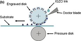
Fig. 9. (a) IGZO solution droplet of inkjet printing.40) (b) Schematic diagram of gravure printing.41)
Download figure:
Standard image High-resolution image5.1. Inkjet printing
Among the coating methods for a solution process, inkjet printing technology is one of the most promising alternatives to vacuum and photolithographic processes. This technology has an advantage that enables direct patterning of thin-film: predetermined area deposition. So, we fabricated inkjet-printed IGZO TFTs which have same structure and annealing condition of spin-coated IGZO TFTs.40) A single piezoelectric dispenser was used for micro-patterning. First, the IGZO solution droplets were jetted having 40 µm of diameter and 35 pl of volume. Next, we applied an electrical voltage to piezoelectric material, then we could control droplet shapes and achieve micro-patterning. This inkjet-printed IGZO TFT had a μFET of ∼0.03 cm2 V−1 s−1 and an on/off ratio ∼104. Although these parameters are poor compared with those of spin-coated IGZO TFT yet, if non-uniformity problem is solved, inkjet printing could be promising method that enables printed TFTs with non-photolithographic and non-vacuum deposition technology.
5.2. Gravure printing
We investigated IGZO TFT using other printing technology "gravure".41) Because gravure technology is direct roll-to-roll printing, it exhibits high throughput and resolution compared with offset printing technologies. There is two factors which are can change printed results, printing speed and pressure between engraved disk and pressure disk. When printing speed is too low, superposition of printing pattern problem is occurred. On the other hand speed is too high, printed surface is not efficiently smooth and clean caused by lack of ink. The role of printing pressure is doctoring of excess ink and transferring of ink to substrate. If pressure is too low, also superstition problem would occur. So we obtained optimal value to make IGZO TFT in our study, 0.4 m/s of speed, 400 N of pressure. The μFET of 0.81 cm2 V−1 s−1 and on/off ratio of ∼106 were obtained. Therefore, gravure printing is a good candidate of simple and high performance process.
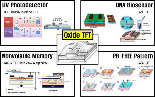
6. Multi-functional solution-processed oxide TFTs
Oxide semiconductors have many advantages including excellent optical and electrical characteristics. In this regards, the oxide TFTs can be applied in various fields such as display, photodetector, biosensor, memory, and so on. In this section, the various applications (see Fig. 10) of solution-processed oxide TFTs with the exception of displays are reviewed.
Fig. 10. Multi-functional solution-processed oxide TFTs: UV photodetector, DNA biosensor, nonvolatile memory, and photopatternable solution.
Download figure:
Standard image High-resolution image
6.1. UV photodetector: IGZO/SWNTs blend TFT
The optical and electrical properties of solution-processed IGZO/single-walled carbon nanotube (IGZO/SWNT) blend TFTs as a function of wavelength (UV 350 nm, blue 450 nm, green 550 nm, and red 660 nm) were investigated.42) The light with wavelength below 550 nm (above 2.25 eV) was strongly absorbed and had a strong effect on the transfer characteristics of IGZO/SWNT blend TFT because the light generated a large density of electron–hole pairs in the active layer. The IGZO/SWNT blend TFTs were incredibly sensitive above 2.25 eV, with deep-level defects at approximately 2.25 eV near the midgap. The photoresponse was explained by using two models: the presence of deep-level traps in the middle of the band gap and the role of SWNTs in increasing the absorption of photons. From the photosensitivity (signal-to-noise ratio) results, the IGZO/SWNT blend TFTs had a higher photosensitivity (approximately two orders high) below 550 nm (2.25 eV) than the IGZO TFTs. Therefore, these results demonstrate that the solution-processed IGZO/SWNT blend TFT could be a good candidate for UV photodetector.
6.2. DNA biosensor: IGZO TFT
Recently, we reported solution-processed IGZO TFT-based biosensors, which fall within a class of field-effect transistor (FET)-based biosensors, for the first time and manifested that they possessed acceptable sensing capability.43) Incorporating these biosensors into label-free methods yields many advantages such as high sensitivity, direct transduction, and simple and low-cost fabrication.
At first, we investigated the effects of exposing solution-processed IGZO TFTs, intended for biosensor applications, to various solvents such as the nonpolar solvent chlorobenzene and the polar solvents ethanol and deionized (DI) water.44) In all cases, when solvent molecules were dropped and adsorbed on the exposed IGZO channel surfaces, negative Vth and Von shifted and SS degraded, without accompanying μFET degradation. These changes were a function of solvent polarity or electronegativity determined by the dielectric constant. With the exception of the IGZO TFT device exposed to DI water, they all gradually returned to their initial states after 300 min.
In our reports, we used ethanol for restoring and delivering DNA nanostructures.43,45,46) The artificially designed double-crossover (DX) DNA solution was dropped onto the exposed IGZO back-channel surface (sensing area) using micro pipette and air-dried for a few minutes. Then, DX DNA nanostructure was immobilized physically on the exposed IGZO channel. Significant decreases in μFET and Ion, a positive shift of Vth, and a slight increase in SS were observed after DX DNA immobilization. These results were attributed to the negatively charged phosphate groups on the DNA backbone, which generated electrostatic interactions in the IGZO TFT. Moreover, we also investigated the solution-processed IGZO TFTs with MSALs for detecting DX DNA.45) After DX DNA adsorption, a significant increase in SS and a negative shift of Von with an accompanying hump were observed in the transfer characteristics. This sensing behavior was attributed to the MSALs and their middle interfaces. These results indicate that DX DNA nanostructures have a direct effect on the electrical response of IGZO TFTs.
6.3. Nonvolatile memory: MIZO TFT with ZnO and Ag nanoparticles
Unlike organic FET which also demonstrates resistive switching behavior, oxide TFT-memory is not as highly sensitive to oxygen and moisture which could hinder fabrication process from producing a decent memory device. We manifested the potential of inorganic MIZO TFTs as non-volatile resistive switching memory device, by inserting metal nanoparticles (NPs) between channel layer and gate dielectric to act as charges trapping site.47,48)
We uncovered the prospect of MIZO TFTs as non-volatile resistive switching memory device through a "pair method" of doping inorganic ZnO NPs to store charge for use in "Write" and "Erase" modes, and using high dielectric constant ZrHfOx solution-processed gate insulator.47) Firstly, C–V characteristic analysis validated that solution-processed ZrHfOx films, which was coated six times, as the gate dielectric in MIM structure is perfectly capable of performing insulating task with a calculated dielectric constant of 10.8 and low leakage current density of roughly 10−10 A/cm2. Secondly, the ZnO NPs doping modifies density of charge carrier and the film, leading to a declined on/off ratio and deteriorating μFET. Lastly, under −5 to 30 V sweep range at a drain voltage of 10 V, a significant clockwise hysteresis from 1.18 to 7.53 V is observed in device with ZnO NPs. Through the fluctuation of Vth, which represents change in stored charges, memory characteristics can be quantified, and it tells that these trapping sites are not saturated and no external defects are present in sweeping region, as also suggested by non-changing SS value. Memory-wise speaking, the fundamental Write and Erase process are triggered by charging and discharging electrons from ZnO NPs after being applied positive and negative gate bias respectively, as validated by charge-retention test. By pairing the usage of inorganic ZnO NPs, and soluble highly dielectric gate insulator such as ZrHfOx with TFT-processing methodology, this paves a promising secondary approach to achieving reliable and stable, all-solution-based non-volatile memory device.
Furthermore, solution-processed MIZO TFT with Ag NPs also exhibited the Write and Erase operation, notable from the large hysteresis as range of sweep voltage is increased.41) The shift in Vth occurs because Ag NPs traps and de-traps electrons, which acts as stored charges at channel/dielectric interface. When voltage is swept in forward direction (−VG to +VG), electrons that were initially accumulated in interface as a result of VGS are further trapped, disturbing current path hence Vth shifts to positive direction (Write). Conversely, reverse direction (+VG to −VG) voltage sweep de-traps electron at Ag NPs site (Erase). Also evident is the linear relationship between increase of VG and ΔVth, where VG increase from 10 to 30 V results in Vth increase from 5.6 to 16.8 V.
MIZO TFT memory consisted of ZnO (Ag) NPs at ZrHfOx (SiO2) gate dielectric/channel interface successfully exhibited memory device properties of Write and Erase operation, which was triggered by positive and negative pulse of gate bias. Further manipulating the magnitude of VG sweep will widen the memory window (ΔVth), portrayed by prominent clockwise hysteresis where electrons are trapped and de-trapped at gate dielectric/channel interface. In addition, the solution-processed MIZO TFT memory exhibited excellent optical transmittance (>80%) in visible light region (390–780 nm), owing to its large optical band gap of 3.80–3.99 eV, notwithstanding to choice of metal nanoparticles material. This suggests that nonvolatile memory based on oxide TFT may found application in fully transparent low-cost high-performance memory devices.
6.4. Photopatternable solution: IGZO solution
Solution-based materials and processes for the fabrication of electronic devices still require the use of traditional photolithography processes to form the required pattern integration. These processes have demerits: they require the use of chemicals such as photoresists (PR), developers, and removers, which can be toxic; they involve complicated steps and layer-by-layer processing, which have high associated costs; and the patterned films can be degraded because of the chemical damage that takes place during the removal steps.
To overcome these problems, we proposed the formation of UV-assisted directly patternable solution-processed oxide thin-films and successfully fabricated oxide TFTs based on these films.49) IGZO solution that was modified chemically with benzoylacetone (BzAc) was used and the direct photopatterning process for the fabrication of IGZO TFTs. The directly photopatterned IGZO TFT had better electrical characteristics than conventional PR-patterned IGZO TFT. It was attributed to the rapid decomposition of the organic compounds in the IGZO gel-film because of its initial pyrolysis when irradiated with UV light. Therefore, this process should be useful in the high throughput fabrication of solution-processed, oxide TFTs via a PR-free process.
7. Conclusions
To challenge Si-based TFTs, we have extensively studied oxide TFTs in many ways, especially solution process, which has many advantages. For the first step to research oxide TFTs, we varied mole ratio of each atom to optimize precursor composition, and made efforts to replace Ga or introduce optimized carrier suppressor. For fabrication of solution-processed oxide TFTs on flexible substrates, we proposed three methods: channel structure (DAL), precursor engineering, and post annealing process (HPA). In order to improve stability and electrical performances, we introduced MSALs. Then, we presented various coating methods for solution-processed oxide TFTs: spin-coating, inkjet printing, and gravure printing. Not only for research oxide TFTs themself, we applied solution-processed oxide TFTs for UV photodetector, DNA biosensor, nonvolatile memory, and photopatternable TFTs.
In this paper, we strived to go over research history for oxide TFTs in our laboratory. Although researches on solution-processed oxide TFTs are still a lot to be studied, significant improvement has been achieve in last few years. Finally, solution-processed oxide TFTs will become a leading technology not only for display, but also for various applications: photodetector, biosensor, and memory.
Acknowledgement
This work was supported by the National Research Foundation of Korea (NRF) grant funded by the Korean Ministry of Education, Science and Technology (MEST) (No. 2011-0028819).