
Abstract
A pair of grating couplers with apodized structure, sandwiched by metal mirrors, was proposed for inter-layer coupling between multilayer waveguides based on hydrogenated amorphous silicon (a-Si:H). We proved theoretically that the introduction of an apodized grating coupler yields a high coupling efficiency of about 90% even for an inter-layer distance of several micrometers. In addition, this high coupling efficiency was obtained for a large bandwidth by adjusting the grating period.
Export citation and abstract BibTeX RIS
1. Introduction
It is believed that the performance of large-scale integrations (LSIs) will soon reach their physical limit because of the relative delay of the global wires in LSIs. To solve this problem, the electrical wires are expected to be replaced by optical interconnections, which enables large-capacity and high-speed signal transmission.1–3) Silicon (Si) is the best candidate as a platform material for such optical interconnections because it shares platform and process technologies with current Si-LSIs (i.e., Si photonics4–6)). Silicon-wire waveguides are suitable for high-density optical integrated circuits because the high index contrast of Si and SiO2 results in a strong confinement of the signal to the Si waveguide core.7) However, in conventional Si photonics, the silicon-on-insulator substrate usually uses crystalline Si. The design of logic circuits and process sequence can be affected by front-end-process integration in which the optical components are in the same layer level as the CMOS transistors. As an alternative, the bonding of a photonics wafer to an electrical wafer was proposed,8) but this requires the fabrication of another wafer. Therefore, we believe that back-end-process integration, in which the optical layers are integrated after the transistor layer fabrication, may be preferable. Hydrogenated amorphous silicon (a-Si:H) is suitable for such back-end process integration because it can be deposited below 300 °C by plasma-enhanced chemical vapor deposition without damage to the CMOS logic layer,9) although the required temperature for crystalline Si is usually over 1000 °C. Moreover, a-Si:H has a very small extinction-coefficient, i.e., low absorption, in the 1.55-µm band and a high refractive index close to that of crystalline Si. In a recent report, a loss of 1.2 dB/cm was achieved with a wet-etched a-Si:H film.10) For these reasons, we are aiming at the realization of multi-layered optical waveguides consisting of a-Si:H,11,12) which provide higher integration density as well as higher total bandwidth. The a-Si:H multi-layered waveguides can easily be created by depositing alternating layers of a-Si:H and SiO2 films.
For realizing the vertical coupling device between multi-layered waveguides mentioned above, we proposed a structure consisting of a pair of grating couplers.13) The grating coupler is able to couple light at a larger inter-layer distance than other types of inter-layer couplers based on evanescent light14–16) because the inter-layer grating coupler uses the diffraction of light, which can radiate forward independently of the waveguides. In our previous report, we obtained a coupling efficiency of 19% in a three-dimensional (3D) finite-difference time-domain (FDTD) simulation and an experimental efficiency of 22%. We also proposed a coupler structure with metal mirrors placed at the upper and lower sides of a pair of grating couplers. In this structure, a coupling efficiency of 90% (at 1550 nm) was obtained by 3D-FDTD and 83% (at 1590 nm) was demonstrated experimentally at an inter-layer distance of 1 µm.17) However, the coupling efficiency of this structure was very sensitive to the inter-layer distance.
In this paper, we propose the apodization of the inter-layer grating couplers to achieve highly efficient coupling between multi-stacked layers, as well as stability with respect to the distance between them.
2. Design of apodized grating coupler
Figure 1 illustrates the structure of the apodized inter-layer grating couplers. The structure comprises a pair of a-Si:H grating couplers with apodized design and a Au film. Other regions are filled with SiO2. The apodization can be accomplished by modulating the leakage factor at each position of gratings separately by modulating the depth of grooves or the duty ratio Lg/Λ of the gratings,18) where Lg is the length of the thick region within the period Λ, as shown in Fig. 1. Here we adopted the latter method because it can be formed through a simple single dry etching process. By modulating the leakage factor, we can shape the radiation beam profile (power distribution). This apodization method has also been used to achieve a mode-matching condition between the grating coupler and a single-mode fiber.19,20)
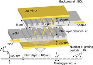
Fig. 1. Structure of inter-layer apodized grating couplers.
Download figure:
Standard image High-resolution imageWe evaluated the coupling efficiency of the inter-layer grating couplers by 2D- and 3D-FDTD simulations. The a-Si:H waveguide width and thickness were set to be 5 µm and 220 nm, respectively, as shown in Fig. 1. A wide-width a-Si:H waveguide was used in order to suppress orthogonal leakage in the radiation beam. The etch depth of the gratings was set to be 100 nm, a value for which we can obtain a large leakage factor. A 200-µm-long linearly tapered waveguide section was employed between the 500-nm-wide wire waveguides and the 5-µm-wide waveguides to avoid reflection and to excite only the fundamental mode in the wide waveguides.13) Metal mirrors were placed at the top and bottom sides of the gratings in order to enhance the coupling efficiency by reflecting the radiated light that leaks outward. We used Au as our metal mirror in this work; however, any kind of metal can be used as long as it maintains a high reflectivity.
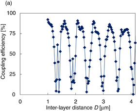
In the case of uniform gratings with the same structure as in our previous work (a grating period of 640 nm, 21 periods, a grating-mirror distance of 800 nm, and a duty ratio of 0.5), the coupling efficiency varied greatly, ranging from 0–90% depending on the inter-layer distance [Fig. 2(a)]. This is because a condition of radiation light depends on the inter-layer distance due to the multiple round-trips between the upper (receiver) side and lower (transmitter) side. The multiple round-trips were caused by mismatch in the radiation-mode profile between gratings at the both sides, as shown in Fig. 3 (blue lines). The radiation-mode profiles of the lower and upper side gratings were monitored by setting power monitors just above and below the grating couplers when there were only one side of a grating and a mirror. In the case of the uniform gratings, the mode profiles are similar to an exponential decay because the leakage factor is fixed. Figure 2(b) shows the E-field distribution in a cross-sectional view of the inter-layer coupling with inter-layer distance D = 3 µm. It includes a pair of grating couplers and mirrors. A TE-mode gaussian light source was introduced at the lower left and the guided mode power at the upper right is observed as output power. The taper between the wire and 5-µm-wide waveguides was not included in the simulation in order to reduce the simulation time, although it would be introduced in actual device fabrication. The blue (red) color in the figure indicates that the E-field is positive (negative). A considerable portion of the input light eventually coupled to the original waveguide (lower waveguide), and so the coupling efficiency to the output waveguide (upper waveguide) became very low (6.8%). We can observe the multiple round-trips in which radiated light travels back and forth numerous times between the upper (receiver) and lower (transmitter) gratings. To eliminate these multiple round-trips, apodization was performed so that the radiation-mode power profile of the lower grating with metal mirror S(z) matched that of the upper grating with metal mirror S'(z). Design sequence of S(z) and S'(z) is described below.
Download figure:
Standard image High-resolution image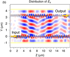
Fig. 2. Simulation results for the uniform grating coupler. (a) Inter-layer distance dependence of coupling efficiency. (b) E-field distribution with D = 3 µm.
Download figure:
Standard image High-resolution image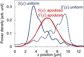
Fig. 3. Beam profiles of radiated light from the gratings. S(z) and S'(z) indicate the profiles of the lower and upper gratings, respectively. The blue and red lines show the results of uniform grating and apodized grating structures, respectively. The distances between grating and metal reflector were set to be 940 and 820 nm for the lower and upper gratings, respectively.
Download figure:
Standard image High-resolution imageThe guided-mode power P(z), leakage factor α(z), and radiated-mode profile S(z) are related through21,22)


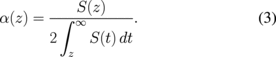
Here, it was assumed that P(0) = 1. Thus, we could calculate α(z) after determining S(z) (or vice versa). We estimated α(z) from Eq. (3) in order to obtain an axisymmetric (with respect to z = 6 µm) radiation-mode profile S(z).
Figure 4 shows the duty-ratio dependence of α(z) estimated by simulating the power decay of the guided mode in a grating with uniform duty ratio in case of putting metal mirror (by using FDTD). We set the duty ratio of the grating coupler based on the estimated α(z) and Fig. 4, but there was a slight difference between estimated S(z) and that simulated using FDTD. Therefore, additional fine-tuning of the duty ratio was carried out manually until the profiles of S(z) became desired shape. Figure 5 shows the flow-chart of the design sequence.

Fig. 4. Designed leakage factor α(z) and calculated radiation beam profile S(x) as a function of z position.
Download figure:
Standard image High-resolution image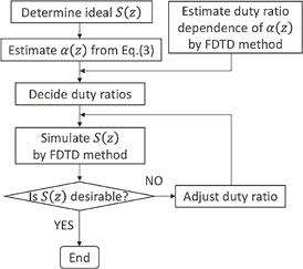
Fig. 5. Flow chart of design sequence of apodization.
Download figure:
Standard image High-resolution imageFigure 6 shows S(z) obtained by FDTD simulation and the α(z) consistent with the duty ratio of grating coupler. The red lines indicate the leakage factor at each position of the individual grating period. The smallest and largest length of the groove was about 30 and 240 nm (for duty ratios of 0.95 and 0.6), respectively.
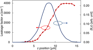
Fig. 6. E-field distribution of the radiation beam from only the lower grating coupler and mirror.
Download figure:
Standard image High-resolution imageAdditionally, the period of the grating was slightly modulated so that the entire beam could be radiated in one direction. This period modulation was required because there was a difference in equivalent refractive index of the guided mode caused by the individual length of the groove. The same process was carried out to derive the radiation-mode profile of the upper grating S'(z). Figure 7 shows the E-field distribution map in the case of only the transmitter (lower layer) grating and lower mirror. To obtain an accurate matching of the beam profile when the distance between two gratings were adjusted, it was necessary to introduce an z-direction offset of 0.2 µm to the receiver grating for every 1-µm layer distance because of the diffraction angle of the radiation beam, which was 79° as shown in Fig. 7. In addition to the apodization of the gratings, the distance between the a-Si:H layer and the metal mirror needed to be adjusted adequately such that the downward and upward radiation beams overlapped in phase. The distance could be determined by the radiation beam power, which was obtained from the simulation, because the radiation power became the largest when the two beams overlap in phase. The appropriate distance to the receiver side (upper layer) was also adjusted in the same manner because of the reciprocity. It was 940 nm at the lower layer and 820 nm at the upper layer, as shown in Fig. 8. In this figure, the radiation power is the ratio of radiation beam power to the input light power. The difference between the distances was caused by the asymmetric structure of these gratings, which resulted in different center positions of the guided modes at the gratings.

Fig. 7. Leakage factor α(z) as a function of the duty ratio of the grating.
Download figure:
Standard image High-resolution image
Fig. 8. Dependence of radiation power on grating-mirror distance. The blue and red lines show the radiation powers from lower and upper gratings, respectively, as a function of grating-mirror distance.
Download figure:
Standard image High-resolution imageAs the results of the above-mentioned design adjustment, the radiation-mode power profile of the lower grating S(z) accorded with that of the upper grating S'(z), as shown in Fig. 3 (red lines). The radiation beam from the lower grating couples to the upper grating, as can be seen in Fig. 9. The E-field between the pair of gratings of Fig. 9 is similar to that of Fig. 7 because there were some multiple round-trips.

Fig. 9. E-field distribution of the inter-layer coupling of an apodized grating coupler with D = 3 µm.
Download figure:
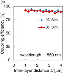
Standard image High-resolution imageThe dependence of coupling efficiency on the inter-layer distance of the designed apodized gratings is plotted in Fig. 10(a). The grating period is 620 nm and the number of periods was 19; these values are close to the ones used in the previous uniform grating structure. A high coupling efficiency of about 90% was obtained, almost independently of the layer distance, by introducing an apodized grating, while the efficiency showed large variations in the case of the uniform grating structure. The reason behind the coupling loss of about 10% is the scattering loss at the grating and the slight mode mismatching of the grating couplers. The discrepancy between the results of the 2D and 3D simulations was caused by a leak in the orthogonal direction (z-direction), although it was very small. The wavelength dependence of the coupling efficiency is shown in Fig. 10(b). In the wavelength range from 1510 to 1570 nm, the coupling efficiency was more than 80%.
Download figure:
Standard image High-resolution image
Fig. 10. Coupling efficiency for a grating period of 620 nm. (a) Inter-layer distance dependence calculated by 2D and 3D FDTD simulations. (b) Wavelength dependence obtained by 2D FDTD simulation.
Download figure:
Standard image High-resolution imageFigure 11 shows the misalignment dependence of the coupling efficiency. The deterioration of the coupling efficiency was relatively small (less than 10%) even with a 1-µm misalignment in both the x- and z-directions. Therefore, the fabrication tolerance is sufficiently large with the conventional lithography methods.

Fig. 11. Misalignment dependence of coupling efficiency for x-direction (dashed line) and z-direction (solid line).
Download figure:
Standard image High-resolution image3. Improvement of coupling bandwidth
The discussion in the previous sections used a grating period of 620 nm for comparison with the previously investigated uniform grating structure. In this section, the method to enhance the wavelength bandwidth will be discussed by controlling the grating period.
One cause of the coupling efficiency deterioration outside the highly efficient coupling wavelength range is the diffraction angle shift of the radiation beam. The diffraction angle θ and the wavelength λ satisfy the following relation:23)

where n denotes the refractive index of the cladding layer, neq the equivalent refractive index of the waveguide, and Λ the period of the grating coupler. A shift in the diffraction angle causes a disagreement in the beam profile between the lower grating and the upper grating. The second cause of the coupling efficiency deterioration is the decrease of the radiation efficiency. Here, the radiation efficiency refers to the conversion efficiency of the light power inside the guided mode to the radiated beam. In the structure of Fig. 1 (620-nm grating period), the deterioration of the coupling efficiency on the short- and long-wavelength sides is mainly due to the first and second cause, respectively.
Thus, we attempted to broaden the coupling wavelength range by adjusting the period of the grating couplers. An analysis of the FDTD simulation shows that the wavelength range of the radiation efficiency is equally broad on the short- and long-wavelength side with a 665-nm period of the grating couplers (Fig. 12). Then, the relative position of the lower and upper gratings was readjusted to obtain an accurate matching of the beam profile at a wavelength of 1550 nm. The duty ratio and the number of grating periods were also readjusted to obtain an accurate symmetric beam profile. The number of grating periods was 21, which was a little more than that of the 620-nm grating-period design, because the leakage factor of the 665-nm grating period is slightly smaller than that of the 620-nm grating period. The wavelength dependence of the coupling efficiency of the structure with a 665-nm grating period obtained using 2D FDTD is shown in Fig. 13(b). A coupling efficiency of more than 80% was obtained for a wavelength range of about 200 nm, which was wider than that of the grating with a period of 620 nm (60 nm). The coupling efficiency was almost independent of the layer distance, similar to the result for the grating with a period of 620 nm, as shown in Fig. 13(a).
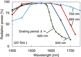
Fig. 12. Wavelength dependence of radiation power (grating periods of 620, 640, 665, and 700 nm).
Download figure:
Standard image High-resolution image
Download figure:
Standard image High-resolution image
Fig. 13. Coupling efficiency of a grating with a period of 665 nm. (a) Inter-layer distance dependence. (b) Wavelength dependence.
Download figure:
Standard image High-resolution image
4. Conclusions
Inter-layer apodized grating couplers with metal mirrors by modulation of the duty ratio of the grating structure were proposed, and their characteristics were evaluated by using FDTD simulation. The coupling characteristics were found to be independent of the layer distance when apodized gratings were used; hence, a constant, high coupling efficiency of 90% was obtained for a layer distance of 1–4 µm. We found that a 665-nm grating period can be used to achieve a coupling efficiency higher than 80% for a broader wavelength range of 200 nm around 1550 nm.
Acknowledgments
This work was supported by the Japan Society for the Promotion of Science KAKENHI Grant Numbers 24246061, 25709026, and 13J08096; and the New Energy and Industrial Technology Development Organization.