
Abstract
Epitaxial growth and electrical properties of γ-Al2O3 films on β-Ga2O3(010) substrates were investigated regarding the prospect of a gate oxide in a β-Ga2O3-based MOSFET. The γ-Al2O3 films grew along the [110] direction and inherited the oxygen sublattice from β-Ga2O3 resulting in the unique in-plane epitaxial relationship of γ-Al2O3![$[\bar{1}10]$](https://content.cld.iop.org/journals/1347-4065/55/12/1202B6/revision1/STAP10005if001.gif) ∥ β-Ga2O3[001]. We found that the γ-Al2O3 layer had a band gap of 7.0 eV and a type-I band alignment with β-Ga2O3 with conduction- and valence-band offsets of 1.9 and 0.5 eV, respectively. A relatively high trap density (≅ 2 × 1012 cm−2 eV−1) was found from the voltage shift of photoassisted capacitance–voltage curves measured for a Au/γ-Al2O3/β-Ga2O3 MOS capacitor. These results indicate good structural and electric properties and some limitations hindering the better understanding of the role of the gate dielectrics (a γ-Al2O3 interface layer naturally crystallized from amorphous Al2O3) in the β-Ga2O3 MOSFET.
∥ β-Ga2O3[001]. We found that the γ-Al2O3 layer had a band gap of 7.0 eV and a type-I band alignment with β-Ga2O3 with conduction- and valence-band offsets of 1.9 and 0.5 eV, respectively. A relatively high trap density (≅ 2 × 1012 cm−2 eV−1) was found from the voltage shift of photoassisted capacitance–voltage curves measured for a Au/γ-Al2O3/β-Ga2O3 MOS capacitor. These results indicate good structural and electric properties and some limitations hindering the better understanding of the role of the gate dielectrics (a γ-Al2O3 interface layer naturally crystallized from amorphous Al2O3) in the β-Ga2O3 MOSFET.
Export citation and abstract BibTeX RIS
1. Introduction
Recently, β-Ga2O3 has been attracting attention as a candidate for future power electronics applications.1–3) Owing to its wide band gap (Eg = 4.4–4.6 eV),4–7) the breakdown electric field is expected to be as high as 8 MV/cm, which would lead to more than three times larger Baliga's figure of merit than those of 4H-SiC and GaN.8) This is a tremendous advantage over its rivals from the viewpoint of practical use. Another advantage of β-Ga2O3 is the compatibility with current fabrication processes of semiconductor devices. Large and high-quality single crystals (≥2 in. in diameter) can be synthesized by melt growth methods such as Czochralski,9) floating-zone,10) and edge-defined film-fed growth.11) Consequently, high-quality β-Ga2O3 homoepitaxial films can be grown by molecular beam epitaxy12,13) and halide vapor phase epitaxy.14) Moreover, the electron density of the epitaxial films can be tuned by impurity levels by controlling the dose of ion implantation15) as well as the source materials.2,13) Using these and other conventional semiconductor-fabrication processes, metal–oxide–semiconductor field-effect transistors (MOSFETs) with a breakdown electric field as high as 755 V have been demonstrated.16)
The quality of the interface between a gate dielectric and β-Ga2O3 is a critical factor for the performance of β-Ga2O3-based MOSFETs. In the aforementioned MOSFETs, atomic-layer-deposited amorphous-Al2O3 layers are used as gate dielectrics, and transistor channels are formed at the β-Ga2O3(010) surface.16,17) By transmission electron microscopy, it has recently been revealed that a metastable γ-Al2O3 layer with nanometer thickness exists at the interface.18) Interestingly, the density of interface trap states correlates with the thickness of the γ-Al2O3 layer. This finding suggests that a metastable γ-Al2O3 layer formed in contact with the β-Ga2O3 surface plays an important role in the device performance. However, the crystallization takes place naturally during device processing, and in such a case, the individual roles of γ-Al2O3 and amorphous-Al2O3 will be discussed only empirically. Moreover, the details of the crystal structure and physical properties of the γ-Al2O3/β-Ga2O3 interface remain unclear. The preparation and characterization of a single-phase γ-Al2O3 epitaxial film on β-Ga2O3 is a direct approach to obtaining useful information for modeling this interface.
In this study, we fabricated γ-Al2O3 epitaxial films on β-Ga2O3(010) substrates by pulsed-laser deposition (PLD) and characterized the epitaxial relationship and the band alignment at the interface. We also investigated photoassisted capacitance–voltage (C–V) characteristics for MOS capacitors with contact metals.
The Al2O3 films were grown on unintentionally doped n-type β-Ga2O3(010) substrates by oxygen-radical-assisted PLD.19) An Al2O3 ceramic target (99.99% purity) was ablated by focused KrF excimer laser pulses at a repetition rate of 10 Hz and a fluence of 0.3 J cm−2. The ablated species were deposited on substrates heated at 500 °C and the oxygen radicals were supplied from a RF plasma cell operated at a RF power of 300 W and an O2 gas flow rate of 0.70 sccm. The typical growth rate was 0.7–0.9 nm min−1.
2. Experimental methods
The techniques and methods used to characterize the samples are as follows. The film thickness and epitaxial structure were evaluated using X-ray reflection and X-ray diffraction (XRD), respectively, with Cu Kα1 radiation (1.540562 Å). X-ray photoemission spectroscopy (XPS) measurements were performed using a VG-Scienta R3000 analyzer with a monochromatized Al Kα X-ray source (1486.6 eV). The C 1s line of the adventitious carbon contamination (284.8 eV) was used to calibrate the binding energy. All spectra were acquired at room temperature with a total energy resolution of 400 meV. The Eg values were estimated by reflection electron energy loss spectroscopy (REELS) at a primary energy of 1 keV as well as from the O 1s loss structure in the XPS spectra. The photoassisted C–V measurement was conducted at a frequency of 1 MHz with the illumination of a Xe lamp (500 W) through a deep-UV optical fiber. The irradiated photon energies (up to 6.2 eV) were sufficient to excite the trapped electrons existing in the entire gap of β-Ga2O3. To excite all the trapped electrons, light illumination was continued until the photocapacitance saturated (the duration was about 2 min). For this measurement, ohmic contact was prepared prior to the γ-Al2O3 growth. A piece of indium metal put on the back of the β-Ga2O3 substrates was partially transferred to an ohmic contact layer through rapid thermal annealing in N2 at 1000 °C for 2 min.20) After the growth, 10-nm-thick transparent Au electrodes with a diameter of 200 µm were vacuum-deposited through a stencil metal mask. A reference C–V curve was taken for a Schottky barrier diode fabricated by the same procedures. All the experiments were carried out at room temperature.
3. Results and discussion
Figure 1(a) shows the out-of-plane XRD pattern of a 28-nm-thick Al2O3 film grown on the β-Ga2O3(010) substrate. Only the 440 reflection of γ-Al2O3 was observed, indicating that the metastable γ-Al2O3 phase was formed under a constraint from the surface lattice of β-Ga2O3(010). The full width at half maximum of the ω-rocking curve of this peak was 0.16°. Figure 1(b) shows a reciprocal space map of the sample, in which the coordinates of QX and QZ are orthogonal to the (100) and (010) surfaces of β-Ga2O3, respectively. The diffraction spots from the 420 reflection of β-Ga2O3 and the 444 reflection of γ-Al2O3 were clearly observed. Taking this finding and the out-of-plane epitaxial relationship of γ-Al2O3(110) ∥ β-Ga2O3(010) into account, the in-plane epitaxial relationship is γ-Al2O3![$[\bar{1}10]$](https://content.cld.iop.org/journals/1347-4065/55/12/1202B6/revision1/STAP10005if002.gif) ∥ β-Ga2O3[001]. Furthermore, these two diffractions from γ-Al2O3 444 and β-Ga2O3 420 exhibited similar ϕ-scan profiles with a twofold rotational symmetry [see Fig. 1(c)]. This result indicates that a single-crystalline γ-Al2O3 film was epitaxially grown on the β-Ga2O3(010) substrate.
∥ β-Ga2O3[001]. Furthermore, these two diffractions from γ-Al2O3 444 and β-Ga2O3 420 exhibited similar ϕ-scan profiles with a twofold rotational symmetry [see Fig. 1(c)]. This result indicates that a single-crystalline γ-Al2O3 film was epitaxially grown on the β-Ga2O3(010) substrate.
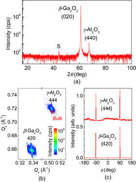
Fig. 1. (a) Out-of-plane XRD pattern of the γ-Al2O3 film grown on β-Ga2O3 substrate. S indicates a reflection from the sample stage. (b) Reciprocal space map around γ-Al2O3 444 and β-Ga2O3 420 diffraction spots. The coordinates of QX and QZ are orthogonal to the (100) and (010) surfaces of β-Ga2O3, respectively. A cross indicates γ-Al2O3 444, corresponding to lattice parameters of bulk. (c) ϕ-scan profiles of asymmetric reflections from the γ-Al2O3 film and the β-Ga2O3 substrate.
Download figure:
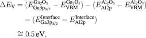
Standard image High-resolution imageDespite different symmetries of the unit cells (cubic γ-Al2O321) and monoclinic β-Ga2O322)), no other rotational domain was found, and thus the film consisted of only a single domain. This unique epitaxial relationship can be understood by taking the arrangements of oxygen sublattices at the film/substrate interface into account. We note that the crystal structures of γ-Al2O3 (as well as γ-Ga2O3) and β-Ga2O3 resemble each other and both are derived from a spinel-type structure (the former is often referred to as the defect spinel-type structure).23) Both of them have cubic-close-packed oxygen sublattices and cations occupy tetrahedral and octahedral sites. Figure 2 illustrates the observed epitaxial relationship with an emphasis on the oxygen sublattices on γ-Al2O3(110) and β-Ga2O3(010). Apparently, they are almost identical to each other. The mismatches of appropriate length in oxygen sublattices ( and Lc along the two orthogonal directions of a* and c of β-Ga2O3, respectively) can be defined by the following equations using lattice parameters of γ-Al2O3 (a' = 7.911 Å)21) and β-Ga2O3 (a = 12.23, b = 3.04, c = 5.80 Å, and β = 103.7°).22)
Here,  ,
,  ,
,  , and
, and  are average spacings between atomic rows for γ-Al2O3 and β-Ga2O3 along the two directions of a* and c of β-Ga2O3 (see Fig. 2 for details). We note a very small mismatch along the c-direction, which reduces the interface energy and promotes the oxygen sublattices to connect across the interface with preferential orientation.

Fig. 2. Schematic drawings of oxygen atoms on γ-Al2O3(110) and β-Ga2O3(010), representing the observed in-plane epitaxial relationship. Double-headed arrows indicate spacings between each atomic row and  and dc are their averages along a* and c of β-Ga2O3, respectively.
Download figure:
Standard image High-resolution imageThe band alignment at γ-Al2O3/β-Ga2O3 was investigated by a standard procedure using XPS.24) We used three samples, i.e., a pristine β-Ga2O3 substrate, a 22-nm-thick γ-Al2O3 film, and a 2-nm-thick γ-Al2O3 film grown on β-Ga2O3 substrates, to analyze signals independently generated from β-Ga2O3, γ-Al2O3, and their interface, respectively.
We first determined a valence-band offset (ΔEV) at the γ-Al2O3/β-Ga2O3 interface. Figures 3(a)–3(c) show XPS spectra for the three samples. In these spectra, peak energies of core levels were determined by fitting to a Gaussian function, while valence band maximums (VBMs) were estimated by the linear extrapolation of the valence-band edge. By comparing energy differences between the core levels and the VBMs for three spectra, ΔEV can be extracted as
where  and
and  are the peak energies of Ga 3p3/2 and VBM for β-Ga2O3, respectively,
  and
and  are the peak energies of Al 2p and VBM for γ-Al2O3, respectively, and
  and
and  are the peak energies of Ga 3p3/2 and Al 2p at the interface, respectively.

Fig. 3. XPS spectra of (a) Ga 3p3/2 and a valence-band edge for the β-Ga2O3 substrate, (b) Al 2p and a valence-band edge for the 22-nm-thick γ-Al2O3 film, and (c) Ga 3p3/2 and Al 2p for the 2-nm-thick γ-Al2O3 film on the β-Ga2O3 substrate.
Download figure:
Standard image High-resolution imageNext, we evaluated Eg to determine the conduction-band offset (ΔEC). We obtained two sets of XPS and REELS spectra to independently determine the Eg of β-Ga2O3 and γ-Al2O3. Figures 4(a) and 4(b) show XPS spectra near O 1s core levels for the β-Ga2O3 substrate and 22-nm-thick γ-Al2O3 film, respectively. In these spectra, the energy difference between the onset of the loss spectrum and the peak energy of the core level corresponds to Eg; Eg values for β-Ga2O3 ( ) and γ-Al2O3 (
 ) were determined to be 4.6 and 7.0 eV, respectively. We paid attention to the poor signal-to-noise (S/N) ratios, which possibly cause statistical error for an estimate of Eg, in both XPS spectra. Therefore, Eg was also evaluated by REELS, a technique often employed to evaluate the Eg of gate dielectrics.25) Figures 4(c) and 4(d) show REELS spectra of the β-Ga2O3 substrate and γ-Al2O3 film, respectively. The energy difference between a primary peak and the onset energy of the loss spectrum corresponds to the minimum energy of the electronic transition from the valence band to the conduction band, that is, Eg. In this case, S/N ratios of the spectra were sufficiently large to analyze characteristic energies.
  and
and  were also determined to be 4.6 and 7.0 eV, respectively, which coincide with the values determined from XPS spectra. The obtained
  and
and  showed good agreement with the reported values of 4.4–4.64–7) and 7.1 eV,26) respectively. Having determined ΔEV,
  , and
, and  , we calculated ΔEC using
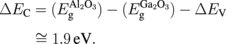
Fig. 4. XPS O 1s loss spectra for (a) the β-Ga2O3 substrate and (b) the 22-nm-thick γ-Al2O3 film, respectively. (c) and (d) are REELS spectra for the same samples as (a) and (b), respectively.
Download figure:
Standard image High-resolution imageThe band alignment at the γ-Al2O3/β-Ga2O3 interface was thereby revealed to be type-I with ΔEC = 1.9 eV and ΔEV = 0.5 eV, which are comparable to those at the amorphous-Al2O3/β-Ga2O3 interface [ΔEC = (1.5–1.6) ± 0.2 eV, ΔEV = 0.7 ± 0.2 eV].27)
Finally, we describe the electrical properties of the γ-Al2O3/β-Ga2O3 interface. Figure 5(a) shows a photoassisted C–V curve measured for a Au/γ-Al2O3/β-Ga2O3 MOS capacitor. First, the carrier accumulation and deep depletion behaviors were clearly observed at positive and negative biases, respectively, which are common features of wide-band-gap-semiconductor-based MOS capacitors. From the saturation value at a positive bias, which corresponds to the capacitance of the γ-Al2O3 layer (Cox), the relative dielectric constant of γ-Al2O3 was calculated to be 6.9 ± 0.2. This value is comparable to the reported value of 7.28) Next, we compared two curves measured with voltage swept down voltage 5 to −15 V in the dark and up to 5 V in the dark after all the trapped electrons were eliminated under illumination at −15 V. In this case, charging and discharging of the average trap states appear in a voltage shift (ΔV).29) Considering the relatively small ΔV ∼ 1 V observed for the Schottky barrier diodes [see Fig. 5(b)], the ΔV ∼ 8 V for the MOS capacitors is attributed not to the bulk β-Ga2O3 but rather to the γ-Al2O3/β-Ga2O3 interface and/or γ-Al2O3. Assuming that the majority of trap states exists at the interface, as is the case for SiO2/SiC29) and AlN/GaN,30) the average density of trap states (Dtrap) can be estimated using29)
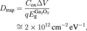
where q is the electron charge. The estimated Dtrap is much larger than those of SiO2/SiC (1.42 × 1011 cm−2 eV−1)29) and AlN/GaN (9.5 × 10¹⁰–1.4 × 1011 cm−2 eV−1).30) The relatively large Dtrap for γ-Al2O3/β-Ga2O3 may be attributed to different crystal structures (namely, relatively large mismatch along the a*-axis) and/or surface damage due to high-energy precursors during PLD.
Fig. 5. Photoassisted C–V curves measured at 1 MHz for (a) Au/γ-Al2O3/β-Ga2O3 MOS capacitor and (b) Au/β-Ga2O3 Schottky barrier diode. Insets show schematic cross sections of the sample structures.
Download figure:
Standard image High-resolution image
4. Conclusions
We fabricated single-phase crystalline γ-Al2O3 epitaxial films on β-Ga2O3(010) substrates to investigate the electric properties of the γ-Al2O3/β-Ga2O3 interface as a model of β-Ga2O3 MOSFETs. The epitaxial relationship between γ-Al2O3 and β-Ga2O3 was clarified, where we observed similar arrangements of oxygen sublattices between γ-Al2O3(110) and β-Ga2O3(010) surfaces. The ΔEV and ΔEC of the γ-Al2O3/β-Ga2O3 interface were revealed to be comparable to those of the amorphous-Al2O3/β-Ga2O3 interface. Despite good structural and electric properties, trap states (≅ 2 × 1012 cm−2 eV−1) were detected by photoassisted C–V measurement. Whether this behavior is intrinsic to the present epitaxial structure or arises from the fabrication process employed in this study remains an open question.
Acknowledgments
The authors thank M. Tada of Center for Advanced Materials Analysis for assistance with REELS, and M. Higashiwaki and T. Kamimura of National Institute of Information and Communications Technology for valuable discussions. This work was supported by a Grant-in-Aid for Scientific Research (No. 26709020) from the Japan Society for the Promotion of Science Foundation, MEXT, the Element Strategy Initiative Project to Form Core Research Center, and a research grant from the Murata Science Foundation.