

Abstract
In this study, we demonstrated a simple method of fabricating a high-performance surface-enhanced Raman scattering (SERS) substrate. Monodispersive SiO2 colloidal spheres were self-assembled on a silicon wafer, and then a silver layer was coated on it to obtain a Ag/SiO2 SERS substrate. The Ag/SiO2 SERS substrates were used to detect three kinds of plasticizer with different concentrations, namely, including bis(2-ethylhexyl)phthalate (DEHP), benzyl butyl phthalate (BBP), and dibutyl phthalate (DBP). The enhancement of Raman scattering intensity caused by surface plasmon resonance can be observed using the Ag/SiO2 SERS substrates. The Ag/SiO2 SERS substrate with a 150-nm-thick silver layer can detect plasticizers, and it satisfies the detection limit of plasticizers at 100 ppm. The developed highly sensitive Ag/SiO2 SERS substrates show a potential for the design and fabrication of functional sensors to identify the harmful plasticizers that plastic products release in daily life.
Export citation and abstract BibTeX RIS
1. Introduction
Surface-enhanced Raman scattering (SERS) spectroscopy was first discovered in 1977,1,2) and widely used for the detection of chemicals, drugs or contaminats.3–13) The intensity of the SERS signal depends on the feature of the periodic metallic nanostructure, including shape, size, and distribution. Since the fabrication techniques for nanomaterials advanced dramatically in the last two decades, several periodic nanostructures can be constructed easily. For example, they can be fabricated by chemical methods for the self-assembly of metallic particles on the substrate or physical processes such as lithography followed by the thermal evaporation of a noble metal.14–20) Metallic nanostructures are usually used to study surface plasmon resonance. Thus, the SERS signal will be enhanced by a strong electromagnetic field owing to localized surface plasmon resonances combined with the vibration intensities of the substances near the metal nanostructures. It can exponentially overcome the detection limit of chemicals.20–27)
A plasticizer is an additive for improving the flexibility, plasticity, or viscosity of a polymer. Phthalate esters, such as dibutyl phthalate (DBP), benzyl butyl phthalate (BBP), and bis(2-ethylhexyl)phthalate (DEHP) are the most commonly used plasticizers. However, these plasticizers might be released from plastic products owing to unstable temperature during use, long-term usage, and critical pH. Once plasticizers are touched and further absorbed by the human body, they could directly affect our health as well as cause severe diseases such as cancer owing to the existence of phthalate ester, which is an endocrine-disrupting chemical (EDC).28,29) Hence, the detection of plasticizers in our daily life should be seriously considered.
In this study, we fabricated a rapidly detecting and highly sensitive SERS substrate built with a monolayer of silver-coated SiO2 spheres on a silicon wafer. The morphology, optical properties, and topography of the Ag layer on the SiO2 sphere were investigated systematically. Furthermore, the as-prepared SERS substrate was used to enhance the intensity of the Raman scattering signal of plasticizers, namely, DEHP, BBP, and DBP. The spectroscopic behavior and enhancement of the Raman scattering signal have been studied.30)
2. Experimental methods
Monodispersive SiO2 colloidal spheres were synthesized by the sol–gel method according to a previous work.31) Tetraethylorthosilicate (TEOS; Acros, 98%) was dissolved in ethanol and then stirred at 30 °C for 30 min. The TEOS solution was mixed with 20 mL of ammonia solution (28–30 wt % solution of NH3 in H2O) and reacted for 2 h. Finally, 380 nm SiO2 spheres were obtained. The SiO2 colloid solution was centrifuged and washed with ethanol to separate the SiO2 spheres from the solution. After washing with ethanol, the SiO2 spheres were dried at 100 °C for 12 h.
The SiO2 spheres (2.0 wt %, ∼380 nm) were dispersed uniformly in a 95% ethanol aqueous solution by ultrasonic treatment. A monolayer structure consisting of amorphous SiO2 spheres was established on a silicon wafer by a spin coating method to prepare the SiO2 sphere array substrate, and it was dried at 80 °C for 24 h. Then, a 150 nm silver layer was deposited on the SiO2 sphere array substrate using a thermal evaporator. Finally, the Ag-coated SiO2 (Ag/SiO2) SERS substrate was obtained. To study the morphology of SERS substrates, all the different kinds of SERS substrates were then observed by field-emission scanning electron microscope (FE-SEM; Elionix ERA-8800FE). Moreover, the topography was analyzed by atomic force microscopy (AFM; Digital Instruments Dimension-3100 Multimode).
The plasticizers detected in this study include BBP (99.9%), DBP (99.9%), and DEHP (99.9%). The chemical structures of these plasticizers are shown in Fig. 1. All of the plasticizers mentioned above with different concentrations were mixed with n-hexane, and then the upper solutions of the plasticizer mixture were spin-coated on the Ag/SiO2 SERS substrate at 5000 rpm. To measure the enhancement of signals in the Raman scattering spectra, these SERS substrates with/without plasticizers were placed on the piezoelectric stage of a micro-Raman spectrometer (WiTec Alpha300S) and excited by a 632.8 nm He–Ne laser (25 mW).
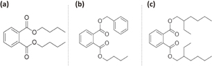
Fig. 1. Chemical structures of various plasticizers: (a) DBP, (b) BBP, and (c) DEHP.
Download figure:
Standard image High-resolution image3. Results and discussion
The various SERS substrates consisting of Ag-coated SiO2 spheres on a silicon wafer were fabricated by spin coating a SiO2 sphere colloid solution at 2000 rpm, followed by the thermal evaporation of silver layers with different thicknesses. The as-prepared SiO2 spheres deposited by self-assembly on the silicon wafer show a uniform monolayer array. The top view of the SiO2 spheres is shown in Fig. 2(a), and the diameter is ∼380 nm. To induce the localized surface plasma resonance (LSPR) and achieve a high surface-enhanced Raman scattering on the SiO2 array substrate, the silver layers with different thicknesses were deposited on the substrate by thermal evaporation. Also, the thickness of the silver layer ranging from 0 to 250 nm can be varied by adjusting the deposition time and each deposition forms a 50-nm-thick silver layer on the SiO2 array substrate. Figures 2(b)–2(g) show the SEM images of the silver layer coated on the SiO2 array substrate with different thicknesses, namely, 50, 100, 150, 200, and 250 nm. As the Ag thickness increases, the gap between the two spheres narrows, and thus the hexagonally arranged SiO2 sphere covered by Ag can be clearly observed. Furthermore, Fig. 3 reveals the cross-sectional SEM images of various Ag/SiO2 SERS substrates coated with the silver layer of different thicknesses. It also indicates that the Ag layer successfully covered the SiO2 spheres after thermal evaporation. Atomic force microscopy was used to investigate the surface morphology of various SERS substrates. Figure 4 shows the topographic image of various SERS substrates with different Ag thicknesses ranging from 0 to 250 nm. We can clearly notice that the interstitial space in the Ag-coated SiO2 sphere array becomes small and the surface roughness decreases with increasing thickness of the silver layer. These results are attributed to the silver nanoparticles that gradually occupied the gap between adjacent silica spheres during thermal evaporation and were filled entirely in each gap. On the basis of morphological and topographical investigations, we surmise a mechanism of silver layer propagation and illustrate a scheme of Ag-coated SiO2 spheres with increasing silver layer thickness, as shown in Fig. 5. Without the thermal evaporation of Ag, the distance between two SiO2 spheres is nearly 50 nm, which is calculated from AFM results. Once Ag was evaporated on the SiO2 spheres and formed a layer of 50 nm thickness, the distance decreased to ∼30 nm. With increasing thickness to 100 nm, the gap was partly occupied by Ag NPs and the distance would be merely ∼10 nm. When the thickness of the silver layer is over 150 nm, the gap was filled and formed a superficial channel. According to a previous study on electromagnetic field calculation by the finite-difference time-domain (FDTD) method, this channel creates the most reliable hotspot to enhance the electromagnetic field.31) Moreover, the optical property of as-prepared SERS substrates was studied and shown in Fig. 6. The normalized absorbance spectra demonstrated that the broad characteristic peak of Ag appears to be redshifted owing to the different extents of coupling between the SiO2 sphere and the Ag surface plasmon resonance. We can observe that the SERS substrate coated with a 150 nm silver layer exhibits a broad peak at a wavelength of ∼640 nm, and it is close to the laser excitation wavelength of 632.8 nm. The more extensive enhancement of surface-enhanced Raman scattering by local surface plasmon resonance coupling with incident laser excitation can be expected. Thus, we adopted the SERS substrate coated with a 150 nm silver layer to detect the plasticizers.
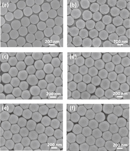
Fig. 2. SEM images of various SERS substrates coated with Ag NP layers of different thicknesses: (a) 0, (b) 50, (c) 100, (d) 150, (e) 200, and (f) 250 nm.
Download figure:
Standard image High-resolution image
Fig. 3. Cross-sectional SEM images of various SERS substrates coated with Ag NP layers of different thicknesses: (a) 0, (b) 50, (c) 100, (d) 150, (e) 200, and (f) 250 nm.
Download figure:
Standard image High-resolution image
Fig. 4. Topographic image of various SERS substrates coated with different silver layer thicknesses: (a) 0, (b) 50, (c) 100, (d) 150, (e) 200, and (f) 250 nm.
Download figure:
Standard image High-resolution image
Fig. 5. Scheme of silver layer progress on various SERS substrates (a) without Ag and with different thicknesses: (b) 50, (c) 100, (d) 150, (e) 200, and (f) 250 nm.
Download figure:
Standard image High-resolution image
Fig. 6. Normalized absorbance spectra of various SERS substrates with different thicknesses.
Download figure:
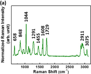
Standard image High-resolution imageTo study the enhancement of SERS substrates for plasticizers, we firstly investigated the Raman scattering of various plasticizers, namely, BBP, DBP, and DEHP. The main structures of BBP, DBP, and DEHP contain phthalate ester. Thus, these plasticizers present similar Raman spectra as shown in Fig. 7. The Raman peaks of DEHP were assigned systematically to C–H stretch, C=O stretch, C=C stretch, C–O stretch, aromatic ring breathing, and C–H bend, which are listed in Table I. The aromatic ring breathing at the Raman shift of 1043 cm−1 exhibits the strongest Raman scattering intensity attributable to the main structure of phthalate. We further choose it to calculate the enhancement factor. The enhancement factor (EF) is defined as

where ISERS_substrate is the intensity of the Raman peak at 1043 cm−1 on the SERS substrate, and Iglass_slide is the intensity of the Raman peak at 1043 cm−1 on the glass slide. To identify the enhancement factor on different substrates, we dropped 10,000 ppm DEHP on a glass slide and silicon wafer, and 1 ppm DEHP on the as-prepared SERS substrate. The Raman spectra for EF on different substrates are shown in Fig. 8. The EFs of the glass and silicon wafer are only 1.00 and 2.24, respectively, whereas that of the as-prepared SERS substrate can reach 21,000.
Download figure:
Standard image High-resolution image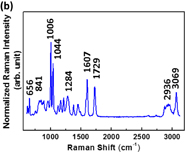
Download figure:
Standard image High-resolution image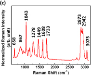
Fig. 7. Raman spectra of various plasticizers: (a) DBP, (b) BBP, and (c) DEHP.
Download figure:
Standard image High-resolution imageTable I. Raman band assignment of DEHP.
| Wavenumber (cm−1) | Band assignment |
|---|---|
| 2873, 2942, 3076 | C–H stretch |
| 1733 | C=O stretch |
| 1608, 1449 | C=C stretch |
| 1278 | C–O stretch |
| 1043 | Aromatic ring breathing |
| 658, 867 | C–H bend |

Download figure:
Standard image High-resolution image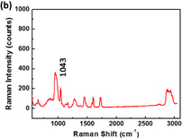
Download figure:
Standard image High-resolution image
Fig. 8. Raman spectra for enhancement factor on different substrates: (a) glass slide, (b) silicon wafer, and (c) SERS substrate.
Download figure:
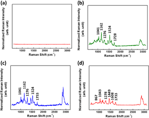
Standard image High-resolution imageFor the plasticizer determination with an interfering substance, the solution of the interfering substance and plasticizers of low concentration was mixed with n-hexane for extraction, and then the upper solution was dropped on the SERS substrate for Raman spectroscopy measurement. The Raman spectra of a series of plasticizers of 100 ppm were studied and shown in Fig. 9. The SERS substrate shows no Raman scattering, and all the plasticizers exhibit a specific C=O stretch band at the Raman shift of 1733 cm−1. It can be attributed to the chemical structure of the phthalate ester containing the C=O bond. Thus, the result indicates that a series of plasticizers involving DBP, BBP, and DEHP can be discovered with the detection limit of 100 ppm.
Fig. 9. Raman spectra of (a) bare SERS substrate, and different plasticizers, namely, (b) DBP, (c) BBP, and (d) DEHP at 100 ppm on SERS substrate.
Download figure:
Standard image High-resolution image
4. Conclusions
In this study, we developed a simple method of fabricating a surface-enhanced Raman scattering substrate by spin coating followed by thermal evaporation. The SERS substrate with monolayer arrays of SiO2 spheres covered by a 150 nm silver layer on a silicon wafer is used to detect various plasticizers, namely, DBP, BBP, and DEHP. The EF of Raman scattering intensity can be 21,000-fold. The detection limit of the as-mentioned plasticizers on the developed Ag/SiO2 SERS substrate can reach 100 ppm. The Ag/SiO2 SERS substrates with low cost, high sensitivity, and quick response display a potential for the design and fabrication of functional sensors to identify the harmful plasticizers that plastic products release in daily life.
Acknowledgements
The authors thank Dr. Ming-Tao Lee of the National Synchrotron Radiation Research Center (BL-13A1) for useful discussion and suggestions. The authors acknowledge the financial support from the Ministry of Science and Technology of Taiwan (MOST 106-2221-E-182-057-MY3, MOST 106-2119-M-002-030, and MOST 106-2632-E-182-001) and Chang Gung Memorial Hospital, Linkou (CMRPD2E0072 and BMRPC74).