

Abstract
We study spin–orbit torque (SOT) switching in W/CoFeB/MgO structures with various dot sizes (120–3500 nm) using pulsed current of various widths τ (800 ps–100 ms) to examine the time and spatial evolution of magnetization switching. We show that the switching behavior and the resultant threshold switching current density Jth strongly depend on device size and pulse width. The switching mode in a 3500 nm dot device changes from probabilistic switching to reproducible partial switching as τ decreases. At τ = 800 ps, Jth becomes more than 3 times larger than that in the long-pulse regime. A decrease in dot size to 700 nm does not significantly change the switching characteristics, suggesting that domain-wall propagation among the nucleated multiple domains governs switching. In contrast, devices with further reduced size (120 nm) show normal full switching with increasing probability with current and insignificant dependence of Jth on τ, indicating that nucleation governs switching.
Export citation and abstract BibTeX RIS
1. Introduction
Spin–orbit torque (SOT)-induced magnetization switching in heavy-metal/ferromagnetic-metal/oxide heterostructures offers a promising information writing scheme for nonvolatile spintronics devices.1–3) For the application of SOT switching in spintronics devices, it is important to elucidate factors that determine the threshold switching current density Jth, especially for nm-scale devices in the nanosecond regime. In our previous work, we investigated Jth in devices patterned from Ta/CoFeB/MgO stacks with a perpendicular easy axis, whose sizes were varied down to the single-domain scale.4) No significant increase in Jth was observed for the single-domain scale device with decreasing pulse width (τ) from the order of microseconds to the nanosecond range, as expected from a macrospin model.5,6) This demonstrates the potential of fast write operation by the SOT switching. On the other hand, it is also important to investigate the time and spatial evolution of SOT switching in devices of larger sizes. The incoherent magnetization reversal behavior in larger devices, characterized by nucleation and domain wall propagation, may become a crucial factor governing switching error rate, which is an important metric for memory applications.7–9) On the other hand, reproducible intermediate switching levels may be beneficial for neuromorphic computing applications.10–12) So far, incoherent reversal has been observed with time-resolved schemes.13–15) It has been pointed out that various parameters, such as effective anisotropy field, Dzyaloshinskii–Moriya interaction (DMI) constant, and field-like component of SOT, dominate the incoherent behavior of magnetization, which strongly depend on the material systems employed.13–17) In this work, we focus on the W/CoFeB/MgO heterostructure, which is one of the prospective material systems in spin–orbitronics owing to the large effective spin Hall angle of W.18–24) An objective of particular interest is to shed light on the time and spatial evolution of switching and the resultant pulse width dependence of Jth for devices of various sizes. On the basis of the obtained results, we discuss how the switching proceeds with time and how the behavior differs depending on the device size.
2. Experimental methods
A stack structure, from the bottom side, composed of W(5)/Co18.75Fe56.25B25(1.3)/MgO(2)/Ta(1) (numbers in parentheses are nominal thickness in nm), is deposited on a highly resistive Si substrate by dc/rf magnetron sputtering. The sputtering power and gas pressure during the deposition of W are 100 W and 0.17 Pa, respectively, under which β-W with a high effective spin Hall angle (∼0.4) was obtained.24) The stack is then processed into two types of devices of different sizes by electron beam lithography and Ar ion milling; one has a cross-shaped Hall bar with a 6000 × 12000 nm2 channel [Fig. 1(a)], and the other has a circular CoFeB/MgO dot (dot device) with various nominal diameters D, formed on top of a cross-shaped W channel of various widths (W) and lengths (L) [Fig. 1(b)]. The results for devices with  ,
,  ,
,  , and
, and  (numbers in parentheses are nominal size in nm) are presented in this article. Cr(5)/Au(100) electrodes are formed at the ends of the channel and Hall probes. The processed devices are annealed at 300 °C for 1 h. Magnetotransport measurement24) reveals that the fabricated devices have a perpendicular easy axis with effective anisotropy fields (
 ) of 0.3–0.4 T (μ0 is the permeability in free space). A schematic of the measurement configuration for SOT switching is shown in Fig. 1(c). Magnetization is switched with a pulsed current I of various widths τ under an external magnetic field of μ0Hx = 20 mT applied collinear to the channel. The direction of magnetization is detected via anomalous Hall resistance RHall using a dc current that is small enough to avoid magnetization reversal.

Fig. 1. Schematics of (a) Hall bar device with 6000 × 12000 nm2 channel; (b) dot device with nominal diameter D, channel width W, and length L; and (c) measurement configuration for SOT-induced switching with the definition of the cartesian coordinate system.
Download figure:
Standard image High-resolution image3. Results and discussion
We first investigate SOT switching in a long-pulse regime (τ = 100 ms) for three devices of different shapes and sizes. We sweep the magnitude of the current I and measure RHall after each pulse application. Figures 2(a)–2(c) show the obtained RHall-J loop, where J represents the current density flowing in the W channel, which is determined from the ratio of the sheet resistance of W to that of CoFeB.10) Jth for SOT switching in the 3500 nm dot device is 0.57 × 10¹² A/m2, which is 9.5 times larger than that in the Hall bar device with the 6000 × 12000 nm2 channel (Jth = 0.06 × 10¹² A/m2). This difference can be understood by considering the effect of the Oersted field25) and the damage on the magnetic layer due to the formation of electrodes. As the dot diameter decreases from 3500 to 120 nm, Jth further increases by a factor of 2.4 (Jth = 1.36 × 10¹² A/m2). The observed difference in Jth between the µm-sized Hall bar [Fig. 2(a)] and the nm-sized dot [Fig. 2(c)] devices is consistent with our previous work on Ta/CoFeB/MgO.4,26) In the following, we investigate the mechanism underlying the difference between the µm-sized [Fig. 2(b)] and nm-sized [Fig. 2(c)] dot devices, which cannot be explained by the Oersted field and damage due to the formation of electrodes.

Fig. 2. Current density J dependence of Hall resistance RHall showing SOT-induced magnetization switching using pulsed current with τ = 100 ms under μ0Hx = 20 mT in devices with (a) 6000 × 12000 nm2 Hall bar device, (b) 3500 nm dot device, and (c) 120 nm dot device.
Download figure:
Standard image High-resolution imageOne possible factor for the difference in Jth is a decrease in  due to Joule heating, which is expected to be proportional to the channel area. Since
  decreases with increasing temperature, Jth may become smaller for larger devices owing to the greater Joule heating. To quantify this effect, we evaluate the device temperature during the current application by measuring the variation in channel resistance with current and the variation in the resistance with temperature. From this evaluation, we find that the device temperature during switching is 55 °C for nm-sized dot samples and 74 °C for µm-sized dot samples. On the other hand, a separate measurement on the temperature dependence of
  reveals that the variation in
  between the two temperatures is 7%. Since this is very small compared with the observed difference in Jth (= 240%), one can conclude that the
  reduction due to Joule heating does not play a dominant role in the observed difference in Jth.
Another possible factor is an effect of incoherent magnetization reversal. For larger devices, the magnetization reversal is expected to start with a nucleation event, followed by a domain wall propagation event, as has been observed in other material systems.13–15) The nucleation event is more likely to take place in larger dots, causing a reduction in Jth. Indeed, intermediate Hall resistances are observed in the 6000 × 12000 nm2 Hall bar [Fig. 2(a)], which indicate an incoherent magnetization reversal in large devices. It is also anticipated that the degree of such an incoherent reversal can be identified by examining the switching in short-pulse regimes, where intermediate RHall levels may be observed owing to the insufficient time for domain wall propagation. This leads us to the study of the SOT switching probability with shorter pulses.
The SOT switching in the short-pulse regime is evaluated as follows: first, the direction of magnetization is initialized to the −z-direction by applying a negative pulsed current I0 under Hx. Then, a positive current pulse I with a specific amplitude and width for magnetization switching is applied. Before and after the switching pulse applications, RHall is measured to examine the magnetization state. This procedure is repeated 10 times to evaluate the switching probability. Figure 3(a) shows an example of the measured results for  = (3500, 6000, and 12000 nm), J = 0.73 × 10¹² A/m2, and τ = 500 ns. Full or partial switching is observed in the second, fifth, and ninth trials. We then analyze the degree of switching by normalizing the difference in RHall between the no- and full-switching states. Figure 3(b) shows the obtained results for increasing J from 0.71 to 0.79 × 10¹² A/m2. Both the switching probability PSW and the degree of switching increase and reach unity with increasing J. Figure 3(c) shows the results for the same device with a reduced τ (= 5 ns), in which a contrasting behavior is observed. In the range J = (1.60–2.01) × 1012 A/m2, partial switching is observed in every trial. Notably, moreover, the degree of switching is reproducible for each J and increases with increasing J.
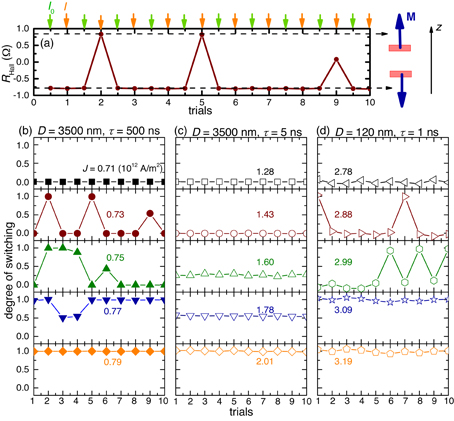
Fig. 3. (a) Example of switching probability measurement for a device with  = (3500, 6000, and 12000 nm) where J = 0.73 × 10¹² A/m2 and τ = 500 ns. After initialization pulse I0 and switching pulse I are applied, RHall is measured. This procedure is repeated 10 times. The difference in RHall before and after the application of I is then normalized by that of full switching to evaluate the degree of switching. Degree of switching for 10 trials for (b)
  = (3500, 6000, and 12000 nm), τ = 500 ns, J = (0.71–0.79) × 1012 A/m2; (c)
  = (3500, 6000, and 12000 nm), τ = 5 ns, J = (1.28–2.01) × 1012 A/m2; and (d)
  = (120, 230, and 1150 nm), τ = 1 ns, J = (2.78–3.19) × 1012 A/m2.
Download figure:
Standard image High-resolution imageThe observed contrasting switching behavior for different τ values can be explained by considering that the nucleation takes place first and is followed by domain wall propagation. For τ = 500 ns, one can infer that the probability of switching is determined by the probability of nucleation, which increases with increasing J. Since full switching is observed at low J values (0.73 × 10¹² A/m2), the 500 ns pulse should be long enough for domain wall(s) to sweep and reverse the whole dot. On the other hand, the partial and reproducible switching observed at τ = 5 ns suggests that the domain wall(s) cannot propagate through the whole dot owing to the limited speed of domain wall propagation, although the pulsed current is large enough to induce nucleation with 100% probability.
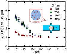
To check the above model, we study the pulse width dependence of Jth over a wide range of τ (= 800 ps–100 µs), where Jth is determined as the current density exceeding PSW = 50%. The obtained Jth is normalized by Jth at τ = 100 µs and is plotted as black squares in Fig. 4. For τ > 100 ns, where probabilistic switching is observed, the variation in Jth with τ is not significant, consistent with the assumption that Jth is governed by nucleation. In contrast, for τ < 100 ns, where partial and reproducible switching is observed, Jth significantly increases with decreasing τ and becomes more than three times larger at τ = 800 ps than that at τ = 800 ns. This result cannot be accounted for by the effect of Joule heating, since the variation in  with τ is found to be less than 14% in a separate measurement. On the other hand, this result can be understood by considering that, in this regime, a sufficiently large current should be applied to displace the domain wall by a required distance during the pulse application; that is, Jth is governed by domain wall propagation. Overall, the pulse width dependence of Jth in the 3500 nm dot device supports the model inferred from Figs. 3(b) and 3(c).
Fig. 4. Pulse width τ dependence of the Jth normalized by Jth at τ = 100 µs in devices with D = 120, 700, 1500, and 3500 nm. The inset shows the nucleated state in the studied systems with D = 700–3500 nm.
Download figure:
Standard image High-resolution image
We now discuss how and where the nucleation occurs. Regarding this matter, two models have been put forward. In the first model, switching starts with a single nucleation event at the edge of the dot and the position is determined by the field-like component of SOT and a torque originating from DMI.14,16) If this is the case, Jth(τ)/Jth(τ = 100 µs) vs τ shown in Fig. 4 should shift to the left as the dot diameter decreases, since the required time for domain wall propagation through the whole dot is reduced as the device is miniaturized. In the second model, the switching starts at multiple nucleation sites within the dot, as shown in the inset of Fig. 4.13) In this case, domain walls only need to travel a small distance among the nucleation sites. Consequently, Jth(τ)/Jth(τ = 100 µs) vs τ would not be governed by the size of the dot but by the distance between the nucleation sites. The measured Jth(τ)/Jth(τ = 100 µs) vs τ plots for devices with the 1500 and 700 nm dot with the same W are shown in Fig. 4 by blue triangles and green diamonds. respectively. No clear difference from the values for the 3500 nm dot is observed, indicating that within the dimensions studied here, the present system is described by the second model.
Finally, we study a dot device with further reduced size  = (120, 230, and 1150 nm), in which much less time for domain wall propagation is expected to be required and thus the required pulse width is determined by the nucleation time. The measured results of the degree of switching by current pulses with τ = 1 ns and various current densities are shown in Fig. 3(d). Probabilistic switching with no intermediate state is seen. Also, Jth(τ)/Jth(τ = 100 µs) of the same device is plotted as the red circles in Fig. 4. A clearly different trend from the results of devices with D = 700–3500 nm can be seen, and the increasing rate of Jth at τ = 800 ps with respect to that at τ = 100 µs is only 1.6. These results indicate that, for a device with D = 120 nm, a multidomain, or partially switched, state rarely appears and switching is governed by nucleation.
4. Conclusions
We have investigated SOT-induced magnetization switching in W/CoFeB/MgO structures of various shapes and sizes using pulsed current with various widths τ. In a long-pulse regime (τ = 100 ms), the threshold switching current density Jth significantly depends on the device shapes and sizes and a 120 nm dot device shows a Jth more than one order of magnitude larger than that of a µm-sized cross-shaped Hall bar device. We have found that the decrease in the effective anisotropy field by Joule heating does not play a major role, suggesting the need to consider the effect of incoherent magnetization reversal, which is expected to be significant in larger devices. In a short-pulse regime, the switching behavior in a 3500 nm dot device changes from probabilistic switching to reproducible and partial switching as τ decreases to less than 100 ns. Here, Jth increases with decreasing τ, suggesting that the speed of domain wall propagation governs the required pulse width. No significant difference in Jth − τ is observed when the size decreases from 3500 to 700 nm, supporting the model that the switching starts from multiple nucleation sites. We have also shown that, for a device with a size of 120 nm, probabilistic and full/none switching appears and the nucleation speed predominantly governs the switching dynamics. In conclusion, the SOT switching shows various behaviors depending on the device shapes/sizes and on the pulse widths used in W/CoFeB/MgO.
Acknowledgments
The authors thank T. Dohi for fruitful discussion and C. Igarashi, T. Hirata, H. Iwanuma, Y. Kawato, and K. Goto for technical support. This work was supported by the R&D project for ICT Key Technology of MEXT, the ImPACT Program of CSTI, JST-OPERA, JSPS KAKENHI Grant Number 17H06093, and RIEC Cooperative Research Projects.