

Abstract
The visualization of localized electronic charges on nanocatalysts is expected to yield fundamental information about catalytic reaction mechanisms. We have developed a high-sensitivity detection technique for the visualization of localized charges on a catalyst and their corresponding electric field distribution, using a low-energy beam of 1 to 5 keV electrons and a high-sensitivity scanning transmission electron microscope (STEM) detector. The highest sensitivity for visualizing a localized electric field was ∼0.08 V/µm at a distance of ∼17 µm from a localized charge at 1 keV of the primary electron energy, and a weak local electric field produced by 200 electrons accumulated on the carbon nanotube (CNT) apex can be visualized. We also observed that Au nanoparticles distributed on a CNT forest tended to accumulate a certain amount of charges, about 150 electrons, at a −2 V bias.
Export citation and abstract BibTeX RIS
1. Introduction
Localized electronic charges on catalysts play an important role in the activation and facilitation of catalytic reactions: platinum nanoparticles on carbon black strongly enhance electrocatalytic reactions such as hydrogen evolution and oxygen reduction for fuel cells owing to charge accumulation on the nanoparticles, and the electrochemical reaction on the surfaces of Pt–CeO2 nanoparticles facilitates electrochemical decomposition of methanol.1–4) A certain amount of charge accumulation at catalytically active sites, and thus, strong localized electric fields, contributes to reducing the overpotential of electrochemical reactions. Moreover, a simple way to induce the accumulation of localized charges is to generate topological defects and protrusions on the surface; thus, controlling defects and undulations on graphene surfaces is a key to the facilitation of electrocatalytic activity.3–7) It has also been reported that high catalytic activities are exhibited by doped nitrogen atoms on surface defects of graphene.7)
Transmission electron microscopy (TEM) has been widely used for the visualization of local electric fields.8–23) For example, visualizing local electric fields by in situ observations of switching in ferroelectric domains has become the recent application of this method to local electric field visualization. The imaging contrast in TEM is related to the deflection of the probing beam in a local electric field; the primary electron beam that passes through a ferroelectric domain is affected by intrinsic polarization and coercive fields, and is thus deflected at a certain angle. Consequently, the projected image features a domain-shaped region of dark contrast in a bright-field image. In situ observations of domain dynamics during switching of multiferroic perovskite ceramics have suggested the use of these materials in resistive random access memory (ReRAM) devices. Although structural transitions in the ferroelectric domain were visualized for coercive field intensities ranging from ∼150 kV/cm (15 V/µm) to 300 kV/cm (30 V/µm) using a 200 keV primary electron beam, structural changes in domains with sizes of about 500 nm are unavoidable.9)
The probing beams deflection angle is inversely proportional to the square of the electron beam energy E. Therefore, lower-energy beams strongly affect the deflection. Consequently, low-energy electron microscopy (LEEM) is a good tool for surface analysis of ferroelectric and ferromagnetic domains on the basis of the detection of backscattered electrons. However, LEEM is not suitable for the visualization of electric field spatial distribution, owing to the imaging principle based on the detection of slight deviations in the trajectories of backscattered electrons.24,25)
Electron beam holography has been widely used for the visualization of local electric and magnetic fields by TEM.8,12–23) In this approach, the primary electron beam is split into reference and object waves as the beam passes through an electron biprism. The electron beam that passes through the specimen gains a phase shift and yields interference fringes on a screen owing to its interference with the reference wave. The distribution of the electric field around a charged specimen also contributes to the phase shift: a local electric field of ∼640 V/µm around a biased carbon nanotube (CNT) apex15) and the field distribution during the field emission from a CNT emitter20,21) were visualized using a 200 keV primary electron beam. Here, higher-precision imaging required a higher acceleration voltage, but there was a tradeoff between beam energy and detection sensitivity.
We previously demonstrated the visualization of local electric fields using a conventional scanning electron microscopy (SEM) system.26–29) We visualized the local electric field induced at the biased tungsten (W) probe by detecting the beam deflection angle of the primary electron beam. The primary electron beam that passed through the localized electric field was strongly deflected and generated deformed grid images; here, the deformation uniquely represented the local field distribution. The beam deflection angle is inversely proportional to beam acceleration voltage, and thus, further decreasing the acceleration voltage markedly improves the detection sensitivity. We also used the low-magnification mode in our SEM system, because the low-magnification mode without the excitation of the main objective lens gains a large focusing depth, which is a tradeoff with the beam convergence in the SEM system. Thus, the low-magnification mode deteriorates the resolution owing to the poor beam convergence, but the SEM system still produces informative field images as the deformed shape of the gold grids, even when the grid is located ∼30 mm downstream of the probe apex.
The electric field induced around the probe apex deflected the primary electron beam and then generated a circularly bent deformation image of the cross-grid detector in the SEM image. Our previous detection technique demonstrated the visualization of the local electric field with an intensity of ∼2.5 V/µm at a 5 keV, but the spatial resolution of that visualization was limited to ∼1 µm.26–28) We need to further improve the detection of localized charges during catalytic reactions. The localized electric field created by a single electron is very weak, ∼0.14 V/µm at a distance of 100 nm from a single localized electron, and collaborative catalytic reactions proceed with several hundreds of electrons maintaining a 10 nm resolution. A higher resolution needs a sharper beam convergence. The high-magnification mode using main objective lens excitation gives a sharp beam convergence for precise imaging. However, the extremely widened beam divergence enormously deteriorates the shape of the grids. Therefore, we introduced a scanning transmission electron microscopy (STEM) detector to capture slight fluctuations of beam intensity to visualize small deflection angles, instead of capturing the deformed shape of the Au grid detector.
On the basis of the same strategy to visualize a local electric field, Shibata and coworkers demonstrated the visualization of an electric field created around a single atom in a SrTiO3 crystal.30,31) A high-energy primary electron beam at 300 keV in a difference phase-contrast (DPC)-STEM system combined with a spherical aberration corrector enabled the visualization of the internal field distribution in a single atom within angstrom resolution through the quadrant-divided STEM detector. However, the ultimate spatial resolution demands ultrathin specimens and a clean environment, which would entail a tradeoff with the versatility in the handling of specimens as well as detection environments, such as detection operation under gas or liquid flow conditions during catalytic reaction.
Each of the detection techniques described above possess merits and demerits depending on the operation and detection range, as summarized in Table I. Here, we demonstrate the high-sensitivity visualization of localized electric field distributions using a high-magnification mode with the excitation of the main objective lens and a high-sensitivity solid-state electron detector. A conventional STEM system is highly useful for visualizing the charge localization in noble-metal nanoparticles, which would be a key to clarifying the catalytic mechanism. Using a low-energy (∼1 keV) electron beam, we visualized field strength under 1 V/µm with a resolution of 10 nm; this field was induced at the W probe/CNT apex.
Table I. Various e-field detection methods and their spatial resolution and detection sensitivity.
| Method | Spatial resolution (nm) | Detection sensitivity of local field intensity (V/µm) |
|---|---|---|
| In situ TEM20) | ∼10 | 1.0 |
| Electron holography22,23) | ∼1 | 10 |
| Near-field optical microscopy32) | ∼300 | ∼20 |
| Previous SEM method26) | ∼100 | ∼2.5 |
| DPC-STEM30,31) | ∼0.1 | N/A |
| Our method | 10–1000 | 1000–0.08 |
2. Experimental methods
We used an S-4800 SEM system (Hitachi) and a high-sensitivity quadrant Si diode-type solid-state STEM detector Gen 5 (Deben). Figure 1 shows the experimental setup. The backpressure of the SEM system was maintained under 10−6 Pa during the experiments. A self-synchronizing lock-in-type amplifier provided a practical gain of up to 106, and the high-frequency response of the detector (up to 5 MHz) enabled rapid imaging in the TV mode (25 frames/s). However, all the field images were collected in the slow-scan mode with a duration of 80 s, and we processed a stack of 4–16 field images to reduce the noise and ensure high imaging quality (see Fig. S1 in the online supplementary data at http://stacks.iop.org/JJAP/57/065201/mmedia). The quadrant detector also enabled two-dimensional deflection analysis. However, small deflections due to a weak field could not drive the beam projection entirely toward the quadrant detector segments. Thus, weak fields were detected using a single-detector segment, which was positioned immediately beside the beam axis.

Fig. 1. Schematic illustration of the experimental setup. (a) Electron optics and the position of the parameter. (b) Beam deflection trajectory depending on the distance from the localized charge. (c) Schematic of the generation mechanism of the deflection shadow; the contours represent the field intensity calculated by FEM simulation. The beam deflection induced at each position flight the same distance along the x-direction and reached the detector's edge line. Inset is the contour of the equivalent field intensity and the original visualized field image by the STEM.
Download figure:
Standard image High-resolution imageIn this study, we defined the deflection length L (typically 13 cm) as the distance between the specimen and the detector. The impact parameter b was defined as the distance from the beam to a local charge (corresponding to the W probe/CNT apex), and the detector distance d was defined as the distance from the central beam axis to the detector edge. We used an electrolytic polishing W probe or CNT for the specimen, and we set up the detector such that a bias voltage could be applied to these specimens. For electron deflection, the Rutherford scattering model was assumed.26,27) The experimental system is shown schematically in Fig. 1(a). In the Rutherford scattering model, the source that generated the electron beam was assumed to be located infinitely far from the system, and it was assumed that the beam had a deviation of impact parameter b, the local charge at the probe apex deflected the beam by the deflection angle θ, and the beam finally reached the STEM detector. The deflection angle θ can be written as

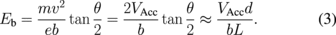
where e is the electron charge, m is the electron mass, v is the electron velocity, Q is the total charge induced at the probe apex, and the permittivity of vacuum is ε0. Considering that the local electric field is
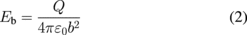
at impact parameter b from the apex, Eb can be related to the acceleration voltage VAcc, the deflection angle θ, and b, as
Excitation of the main objective lens improves the spatial resolution. However, a large beam divergence (up to 1 mm) of the full width at half maximum of the Gaussian beam profile causes contrast blurring at edge of the detector, as shown in Fig. 1(a). The inset shows the schematics of the relationship of deflection at the probe apex with the impact parameter b. Figure 1(b) shows how the scattering angle increases within increasing electric field as it comes closer to the charge.
Figure 1(c) shows the field distribution at the probe calculated by the finite element method (FEM) and the mechanism by which deflection images are created by SEM/STEM. The upper inset shows the visualized image where a bright area appeared just on the biased probe apex at −40 V, and the yellow circular line is a contour line created by same-intensity pixels. Hereafter, we refer to the bright circular area as the deflection shadow. Here, the circular yellow line easily comes to mind when inspecting the distribution of the field at the apex. However, the conducting body of the W probe never generates such a concentric distribution; rather, it generates an similarly shaped distribution in the corresponding FEM simulation.26) Here, we defined the detector's edge to be along the y-axis, while the W probe/CNT body was located along the x-axis. The gradients of the electric field at A, B, and C were different. However, the cosine components of the electric field vectors projected in the direction of the detector-edge normal (horizontal direction) all had the same magnitude. Thus, the primary beam electrons that reached A, B, and C were deflected and traveled the same distance d along the x-axis toward the detector's edge. These electrons reached different positions on the detector's edge; the electrons that scanned point A, where the electric field vector contained only the x component, were deflected to A' on the detector's edge crossing the same probe axis. The electrons that scanned point C, which featured the largest electric field component along the y-axis, exhibited the longest flight to point C' on the detector's edge. The law of cosines for the electric field for projecting in the direction normal to that of the detector's edge is essential for the visualization of local electric fields and explains why a concentric circular shadow appeared against the detector-edge line.
Figure 2 shows the typical changes in the deflection shadows depending on bias voltage and on acceleration voltage. Figures 2(a)–2(d) show the dependence of the shadow shape on bias voltage. The deflection shadow suddenly appears when the bias voltage reaches −36 V, and the shadow sensitively increases with increasing bias voltage. A slight change in bias voltage from −36 to −42 V markedly increases the deflection area, but soon results in a whiteout with overspreading of the shadow throughout the entire imaging field. The edge of the deflection shadow corresponds to the contour of the equivalent field intensity, and the local electric field at the shadow's edge was calculated to ∼3.5 V/µm at the acceleration of 5 keV in Fig. 2(d).
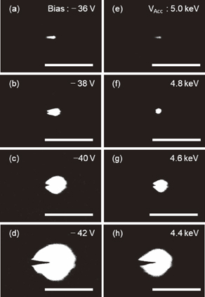
Fig. 2. Dependence of the deflection shadow on the bias voltage applied to the W probe [panels (a) to (d)], and on the acceleration voltage VAcc [panels (e) to (h)]. All scale bars are 10 µm.
Download figure:
Standard image High-resolution imageThe deflection shadow also sensitively depends on acceleration voltage, as shown in Figs. 2(e) to 2(h). The deflection angle is inversely proportional to acceleration voltage, which can be written as

Thus, a slight reduction in the acceleration voltage dVAcc results in a rapid widening of the deflection shadow. Therefore, the boundary of the bright area in Fig. 2(f) corresponds to 18 V/µm, the boundary in Fig. 2(g) to 7.1 V/µm, and the boundary in Fig. 2(h) to 4.7 V/µm at a bias voltage of −30 V.
Here, we operated the STEM system in the low-magnification mode to visualize the local field distribution in the obtained STEM images. The large focusing depth, as well as the small divergence of the primary electron beam in the low-magnification operation of the S-4800 system,26,27) provides another advantage for local field visualization; the primary beam still retains a small divergence even after traveling 13 cm downstream of the detector position from the specimen stage. Thus, the small beam spots at the detector created a relatively sharp contrast in dark-field images depending on the spatial variation of local field intensity, as shown in Fig. 2. However, we need a high-magnification mode to improve the spatial resolution and detection sensitivity for visualizing a small localized charge on the catalyst, which consequently reduces focusing depth and thus causes a large beam divergence at the detector position, which, in turn, inevitably generates blurred deflection shadows. Therefore, we need some numerical processing to convert the pixel brightness information in the recorded STEM images to an electric field intensity distribution.
3. Results and discussion
Figure 3 shows the method to evaluate field intensity using a STEM image. The original STEM image is shown in Fig. 3(a), and Fig. 3(b) shows the corresponding brightness level along the probe axis. Position A is located at the probe apex, having 100% brightness, suggesting that the entire primary beam was projected on the detector. We also determined position B of a beam whose intensity was half the brightness (50% intensity), which is consistent with the fact that the center of the blurred primary beam reached the detector's edge (see Fig. S2 in the online supplementary data at http://stacks.iop.org/JJAP/57/065201/mmedia). Grayscale images were constructed using 256 levels of brightness, and we adjusted the system so that the entire signal of the detector was within this range of grayscale levels, as shown in Fig. 3(b). Then, position B on the STEM image gives the impact parameter of about 600 nm distance from the tip apex to the detector edge. The yellow contour of the local electric field can be visualized by painting the equivalent pixels that have the same 50% brightness. Thus, the yellow contour shown in Fig. 3(c) corresponds to the local field intensity of 15 V/µm for the deflection with a bias voltage of −50 V at 3.0 keV of the primary electron beam. Here, we estimated about 4000 electrons would be accumulated at the probe apex, on the basis of FEM simulation results.
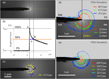
Fig. 3. Analysis method for the local field intensity. (a) Original STEM image, and (b) brightness profile along the yellow line in (a). The impact parameter b was defined by the position B having 50% of the brightness level (128). (c) Contour of the deflection shadow occupying 50% intensity of brightness. (d) Contour mapping of 20, 13, and 8 V/µm field intensities by superimposing the contours determined from different acceleration voltages of 2.5, 2.4, and 2.3 kV, respectively. Upper quadrant is FEM simulation. (e) Contour mapping of 200, 100, 50, 20, and 10 V/µm field intensities derived from a single STEM image and point charge model.
Download figure:
Standard image High-resolution imageWe carried out two types of analysis; one involves the superposition of contours taken from each acceleration voltage, and the other the creation of contours from brightness level analysis based on the point charge model. Now a contour map of local field intensity can be constructed by superimposing the contours of all STEM images at acceleration voltages of 2.5, 2.4, and 2.3 keV, as shown in the half bottom of Fig. 3(d). The probe bias is −50 V. Here, the red contour corresponds to the field intensity of 20 V/µm calculated from the impact parameter b of 427 nm at 2.5 keV of primary electrons, the field intensity of 13 V/µm with the impact parameter b of 613 nm for 2.4 keV, and the field intensity of 8 V/µm with the impact parameter b of 764 nm for 2.3 keV.
The rectangular area of the upper half of Fig. 3(d) shows the contours calculated from FEM simulation. The FEM simulation explains well the field intensity distribution. In particular, the simulated intensity along the central probe axis agrees well with the measured value. The shape of the contour and its position derived from the FEM simulation agree well with those obtained from the STEM image, especially in the right-side area (1st and 4th quadrants), as shown in Fig. 3(d). However, the intensity deviation increases with increasing distance from the probe apex around the probe body, in particular, in the left area (2nd and 3rd quadrants of the coordinate origin of the probe apex). We believe that with a slight misalignment of the probe axis from the detector normal, the probe axis would have a small anticlockwise rotation angle, which may generate asymmetric shadows. Also, the beam scattering beside the probe body no longer follows the Rutherford scattering scheme, and the circular detector shows higher detection sensitivity for the deflected beam toward the circumferential direction from the probe axis (see Fig. S3 in the online supplementary data at http://stacks.iop.org/JJAP/57/065201/mmedia). The number of charges at the probe apex was estimated to be about 2500 electrons using Eqs. (2) and (3).
In contrast, a contour map can be created from a single image by brightness-level analysis. The lower half in Fig. 3(e) shows the contour map created using the same brightness levels from a single STEM image. The illuminated net area of the deflected electron beam can be interpreted from the gray scale intensity as long as the illuminated area remains on the detector edge. Then, a small variation in the brightness level may be proportional to the deflection angle, and thus the brightness level is directly related to local field intensity.
Here, we assume a certain number of point charges were accumulated at the probe apex, and the half-intensity position gives about 20 V/µm, considering an impact parameter of about 420 nm. Here, the acceleration of the primary electron beam was 2.5 keV, and the probe bias was −50 V. The light blue contour has the 50% brightness (120 level) as the reference intensity, where an impact parameter b of 420 nm was defined from the STEM image, and the local field intensity was estimated to be 20 V/µm using Eq. (1). Assuming a charge accumulation of about 2500 electrons at the tip apex and a reference intensity at 20 V/µm, the entire field intensity in the STEM image is analytically determined using the simple point charge model in terms of brightness level. Thus, the brightness level of 176 having the impact parameter b of 131 nm corresponds to 200 V/µm, that of 152 corresponds to 100 V/µm, that of 135 corresponds to 50 V/µm, and that of 109 corresponds to 10 V/µm. The FEM simulation shown in the upper half in Fig. 3(e) explains well the experimental data within the range from 10 to 200 V/µm (see Fig. S4 in the online supplementary data at http://stacks.iop.org/JJAP/57/065201/mmedia).
Lowering the acceleration voltage should improve the detection limit of the local field intensity. Our previous technique using a gold grid was carried out with the primary electron beam of 5 to 10 keV without the excitation of the main objective lens (low-magnification mode), and the local electric field of 2.5 V/µm was visualized through the deformation of the grid shape.
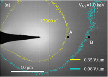
Figure 4(a) shows a typical visualized image at low field intensity, and (b) shows the intensity diagram along the probe axis, where the yellow contour suggests a field intensity of 0.35 V/µm at a primary beam of 1 keV with the excitation of the objective lens (high-magnification mode). Here, the impact parameter was 8.5 µm for the half-intensity of brightness at position A and the STEM magnification power was 3000. The highest sensitivity would be defined by the minimum detectable brightness level, which should be distinguished from the substantial signal/noise ratio. The field intensity at position B in Fig. 4(b) was about 0.08 V/µm at a distance of about 17 µm from the apex, which corresponds to the position having the 35% brightness level with a 2% signal fluctuation amplitude. The high-magnification mode is useful for detecting a weak local field that is beyond the detection limit of the gold grid deformation.26)
Download figure:
Standard image High-resolution image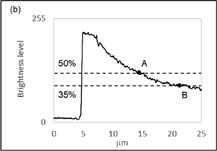
Fig. 4. (a) Visualized local electric field around W probe apex at −30 V of biasing voltage, and (b) brightness profile along the probe axis. The yellow contour is electric field strength of 0.35 V/µm determined at half-brightness, and the light blue contour indicates the 0.08 V/µm region.
Download figure:
Standard image High-resolution imageThe spatial distribution of the local electric field should affect the beam trajectories and deforms the beam spreading on the detector surface. Thus, the projected bright field on the detector should have a certain distortion from the circular shape. We estimate the spot of the primary beam of 3 keV to be about 20 nm from the resolution of the SEM image in Fig. 3(c), and the beam spreading on the detector to be about 800 µm in diameter. However, the local field intensity differs even within 20 nm of the beam spot area. The difference in the deflection angle between the electron that passed by the point nearest to the point charge and that most distant from the point charge should create a distortion of the beam projection. The distortion should be about 8 µm, and the bright-field area on the detector surface resulting from the difference in the amount of deflection within the spot is within 2% (details in supplementary discussion). The brightness level represents the integrated the electron yield on the detector surface. However, the Gaussian intensity distribution shows the maximum intensity at the center. Thus, the distortion effect could be small enough for field evaluation.
One practical advantage of our technique is that it enables multipoint imaging of local charges randomly distributed on a CNT apex in the forest. Figure 5(a) shows a SEM image of the target area of the CNT forest, where each CNT apex was projected to white fibers using a 3 keV primary electron beam. Figure 5(b) shows a STEM image of the localized field taken with the application of a bias voltage of −50 V to CNT. Here, the low-energy primary beam projected the CNT body as the dark contrast resulting from the electrical shielding of the primary electron beam, and deflection shadows appeared at each apex of the CNT. The size of the white shadow area depended on the total number of accumulated charges at the apex, and the estimated number of charges was distributed to be about 670 to 2000 electrons. Using the high-magnification mode of the Hitachi S-4800 SEM system substantially improved the spatial resolution (up to ∼10 nm) as well as the sensitivity. Also, the detection sensitivity was considerably improved by reducing the acceleration voltage to 1 keV. Figure 5(c) shows the magnified field image corresponding the yellow rectangle in Fig. 5(b). We also decreased the biasing potential to −30 V. Then, the STEM image revealed that localized charges of about 200 electrons were accumulated at the apex, and a local field of 100 V/µm was created at 55 nm from the apex. Note that the local electric field of 100 V/µm corresponds to a strong field intensity, but the detecting position of 55 nm was very close to the localized charge (see Fig. S5 in the online supplementary data at http://stacks.iop.org/JJAP/57/065201/mmedia), and the electric field rapidly decreased to below 0.3 V/µm at a distance of 1 µm from the apex. Thus, the balance between high-sensitivity and spatial resolution is required to detect localized charges.

Fig. 5. Visualizations of the multipoint imaging of local charges distributed on the CNT apex in the forest. (a) SEM image at the target area, and (b) STEM image at −50 V bias voltage applied to the CNT forest. (c) Magnified STEM image taken at −30 V bias voltage under 1.0 keV primary beam acceleration. The deflection shadow was generated by about 200 electrons and created 100 V/µm of local field intensity at 55 nm from the apex.
Download figure:
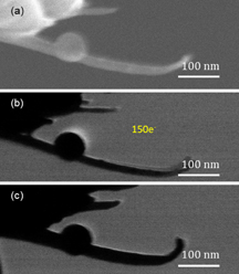
Standard image High-resolution imageWe also succeeded in visualizing the localized electric field generated near the metal nanoparticles embedded on a CNT as an applicable structural model of the carbon-based catalytic electrode. We coated the Au particles onto CNT by a sputtering technique, and visualized the local electric field around the metal particle, as shown in Fig. 6. Here, we adjusted the acceleration voltage of the primary electron to be 5 keV to achieve the highest spatial resolution balancing with the highest sensitivity. Figure 6(a) shows conventional SEM images of a gold particle on the CNT with external bias voltage of −2 V, and Fig. 6(b) shows the STEM image with the same bias voltage.
Fig. 6. Local electric field visualization around Au nanoparticle supported on CNT fiber. (a) SEM image of Au on the CNT fiber, (b) local electric field appearing around the Au nanoparticle with −2 V bias voltage, and (c) disappearance of deflection shadow upon disconnection of bias voltage.
Download figure:
Standard image High-resolution image
We observed neither specific features around the SEM images due to a charging effect from the irradiated electron beam nor specific deformation of the gold nanoparticles embedded in the CNT body regardless of the biasing potential. Thus, the SEM images suggest that the charging effect was almost negligible in the CNT specimen. However, the −2 V bias exactly created a markedly bright area around the gold nanoparticles in the STEM image. The bright area suggests that the accumulation of a certain amount of charge was induced by the bias voltage of −2 V, while none of the specific bright spots appeared on the apex of the CNT in Fig. 6(b). The local electric field intensity was estimated to be about 550 V/µm at a distance of 20 nm, and the accumulated charges were about 150 electrons.
In contrast, a STEM image of the same position shows none of the deflection shadows around a nanoparticle, as shown in Fig. 6(c), suggesting that bright spots indicate that the appearance of localized charges were triggered by −2 V bias voltage. We rubbed the CNT specimen on a copper mesh before coating Au particles onto the CNT. Thus, the CNT would have good electric conductivity between the copper mesh and the CNT. Charge accumulation or charge-up of the specimen commonly occurs during SEM observation. However, our visualized field image suggests that metal particles supported on a conductive CNT tend to accumulate preferentially a certain number of charges rather than the conductive surface of CNT. An amorphous layer that covers the CNT surface would frequently function as a high-resistivity interlayer conductor, and we believe the high-resistivity layer may be the origin of the local charge accumulation on the metal nanoparticle. Such strongly localized charges would be the key to understanding the catalytic mechanism of metallic nanoparticles.
We carried out FEM simulation using the Laplace equation based on a cylindrical coordinate system around the probe axis. Thus, the contour line derived from FEM simulation represents the field intensity distribution on the horizontal cross section including the probe axis. The analytical formula of the Rutherford scattering involves the spatial distribution of the electric field along z-direction (beam incident direction). However, the effective thickness of the electric field is very small, about the same order as the impact parameter, from ∼50 nm to 10 µm, but the thickness is much smaller than the scattering length L. Therefore, the beam trajectory forms a hyperbolic line having an acute angle at the probe apex. The thin layer of the effective electric field containing the probe axis contributes to beam deflection, and thus the FEM simulation agrees well with the field distribution of the thin effective layer. Our visualization method can be extended to the reconstruction of a true three-dimensional distribution image by superimposing the tilted imaging plane.
4. Conclusions
We demonstrated a high-sensitivity visualization technique for the local electric field, using low-energy electron beam deflection and a high-sensitivity solid-state STEM detector. The local electric field distribution represented the cosine component of the electric field along the direction of the detector edge normal. Thus, a symmetric circular shadow appeared on the CNT apex. We visualized the weak field of ∼0.08 V/µm at a 1 keV primary electron beam, and we also detected the charge accumulation of ∼200 electrons at the CNT apex, where the localized field intensity was about 100 V/µm at 55 nm from the CNT apex. We also observed the charge accumulation on noble-metal particles supported on the CNT body, where about 150 electrons accumulated, and the charge created the local field of about 550 V/µm at a distance of 20 nm. We believe that our visualizing method is a powerful technique for clarifying the catalytic reaction mechanism by visualizing the localized charges during catalysis.
Acknowledgment
This work was supported by the Ministry of Education, Culture, Sports, Science and Technology of Japan (MEXT) through Grants-in-Aid for Scientific Research (Grant Nos. 23246063, JP15K13717, and JP15H02195).