

Abstract
We demonstrated non-destructive and non-contact measurement of semiconductor optical waveguide using optical coherence tomography with a visible broadband light source (vis-OCT). Vis-OCT can provide high axial and lateral resolutions of less than 1 µm, which were effective for measurement of optical waveguides with several-micrometer structure. We obtained cross-sectional images of ridge-type optical waveguides (RWGs) fabricated as test samples and measured the height and width of the RWGs. The height and width measured by vis-OCT were similar to these values measured by scanning electron microscopy. These results indicated that vis-OCT enables measurement of the height and width of optical waveguides without destruction and contact, which is a useful inspection method for high-quality and high-efficiency integrated optical device fabrications.
Export citation and abstract BibTeX RIS
1. Introduction
With the recent progress of integrated photonic device technology, such as photonic integrated circuits (PICs),1) non-destructive and high-resolution metrology have become the key technologies for improving device quality and reliability. The PIC consists of integrated optical components connected with optical waveguides, e.g., ridge-type optical waveguides (RWGs), with a several- to sub-micrometer scale to propagate single mode light in C-band.2–6) Thus, the structural accuracy of fabricated waveguides according to the designed dimensions is significant for reducing their propagation loss and stabilizing the mode profile, which increase the efficiency and reliability of the PIC. To realize structurally accurate waveguides, a high-resolution inspection of the fabricated waveguides is necessary. So far, scanning electron microscopy (SEM) or a step profiler have been frequently used to inspect the height and width of the fabricated waveguides; however, these measurement methods are destructive or require contact with the sample. Development of a non-destructive and non-contact measurement method with high spatial resolution is thus required.
To meet the requirement, we have focused on optical coherence tomography (OCT)7) with a visible broadband light source, that is, vis-OCT.8–12) OCT is well known as a high-resolution, non-destructive, and non-contact profile imaging technology, particularly in medical use. The axial resolution (Δz) of the OCT image depends on the center wavelength (λ0) and bandwidth (Δλ) of the light source, for example, Δz when using a light source with a Gaussian spectrum shape can be expressed as

where n is the reflective index of the sample.13) For achieving higher axial resolution, a light source with shorter λ0 and larger Δλ is necessary. OCT has been developed in the medical fields; however, it has also been applied as a new imaging technology for industrial products,14–20) such as silicon integrated circuits,14) light-emitting diodes,15) and automotive paints,16) in recent years. These studies demonstrated the usefulness of OCT for evaluation and fault inspection of fabricated products; however, products with several-micrometer structures have not been measured and evaluated by OCT. If it is possible to measure the structures of such fabricated products using OCT, OCT can find widespread application in various fields. Therefore, we demonstrated a new method for the measurement of optical waveguides by using OCT with high spatial resolution.
In this study, we utilize vis-OCT to improve high axial resolution for the measurement of several-micrometer structures of RWGs. Although a near-infrared (NIR) light source is frequently used for medical use to avoid absorption by hemoglobin and water, and allow its deep penetration in biological samples,21,22) a visible broadband light source is available as a low-coherence light source for application in industrial fields. Vis-OCT provides higher axial resolution than NIR-OCT as expressed in Eq. (1). We have already developed vis-OCT with axial resolution of less than 1 µm and have demonstrated profile measurement of a semiconductor thin layer.12) In this work, we improved the lateral resolution of vis-OCT by using high numerical aperture (NA) objective lenses and evaluated vis-OCT for RWG inspection by demonstrating non-destructive and non-contact measurements for fabricated semiconductor RWGs.
2. Experimental methods
2.1. Optical waveguide fabrication
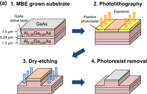
Semiconductor RWGs were fabricated as test samples using conventional photolithography and dry-etching processes. As shown in Fig. 1(a), a wafer with a 0.24-µm-thick waveguide layer of GaAs sandwiched between 1.5-µm-thick Al0.35Ga0.65As cladding layers was grown by molecular beam epitaxy. Such stacked semiconductor layers which have different refractive indices are frequently used for optical confinement in a semiconductor optical device such as an edge-emitting light source.23–26) To avoid oxidization, the upper AlGaAs cladding layer was capped with a 20-nm-thick GaAs layer. After line and space patterns were drawn on the grown GaAs/AlGaAs wafer by photolithography using positive photoresist (Microchemicals AZ5214E), RWG structures with nominal widths of 100, 50, 25, 5, and 3 µm were fabricated by inductively coupled plasma reactive ion etching (ICP-RIE). The nominal etching height was 1.5 µm. Both ends were cleaved and RWGs approximately 8 mm in length were prepared. Figure 1(b) shows a panoramic view of the SEM image of the fabricated 3-µm-wide RWG.
Download figure:
Standard image High-resolution image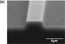
Fig. 1. (a) Schematic of the RWG fabrication processes. (b) SEM image of the 3-µm-wide RWG.
Download figure:
Standard image High-resolution image2.2. Spectral-domain vis-OCT
Vis-OCT was constructed based on a spectral-domain (SD)-OCT system, as shown in Fig. 2(a). The SD-OCT system enables measurement of reflectivity distribution along the incident light axis (depth profile) from the inverse Fourier-transformed (IFT) interference spectrum between the reflected light from the sample and a reference mirror.27) A halogen lamp coupled with a single-mode fiber (SMF) of approximately 4.0 µm core diameter was used as the visible broadband light source. Figure 2(b) shows a spectrum of the visible broadband light source obtained from the reflection from the reference mirror. The center wavelength was 662 nm and the full width at half maximum (FWHM) was 287 nm. The introduced light was collimated through an objective lens (f = 11.7 mm) and split by a beam splitter (BS) into a sample arm and a reference arm. Each split light was focused on the sample and the reference mirror by a high NA (0.50) objective lens with the plan apochromatic aberration correction applied from the visible to near-infrared wavelength region (Mitutoyo M Plan Apo NIR 100x, f = 2.0 mm). By using this objective lens, the spot size of each focused beam can be reduced, which is estimated to be approximately 0.68 µm in diameter without degradation of the axial resolution due to the aberration. This spot size is approximately 5–7 times smaller than that in our previous vis-OCT system with conventional achromatic lenses (NA = 0.4).28) The reflections from the sample and the reference mirror were recombined by the BS and the interfered signal was focused by an achromatic lens (f = 80 mm) into a spectrometer. The interference spectrum was detected by the spectrometer with an exposure time of approximately 100 ms. By calculating the IFT interference spectrum, a depth profile was obtained. A two-dimensional OCT image was then produced by scanning the probe light in steps of 0.2 µm in the lateral direction across the RWG structure. The cross-sectional vis-OCT measurements and imaging were performed on several positions on the RWG to check the variation in width and height.

Download figure:
Standard image High-resolution image
Download figure:
Standard image High-resolution image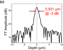
Fig. 2. (a) Schematic of the vis-OCT setup. (b) Spectrum of the visible broadband light source. (c) PSF obtained from the IFT interference spectrum between the reflections from the reference mirror and an identical mirror set on the sample stage.
Download figure:
Standard image High-resolution imageThe axial resolution of the SD-OCT system can be estimated from the point spread function (PSF) of the light source obtained from the IFT interference spectrum between the reflections from the reference mirror and an identical mirror set on the sample stage. The PSF of the light source is presented in Fig. 2(c), and the FWHM of the PSF, which corresponds to the axial resolution, was approximately 0.93 µm.
To evaluate the accuracy of the vis-OCT measurements, the measured width and height values of the fabricated RWGs were compared with those obtained by SEM (JEOL JSM-6390) with an acceleration voltage of 20 kV. The SEM observations were performed for cleaved edges of the RWGs.
3. Results and discussion
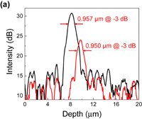
Figure 3(a) shows typical depth profile curves obtained by vis-OCT with a probe axis fixed on the RWG (black line) and the substrate at the side of the RWG (red line). Each profile indicates a peak with a line width of approximately 0.95–0.96 µm, which can be caused by the reflection from the surfaces of the sample, and the line width almost corresponds to that of the PSF of the light source, as shown in Fig. 2(c). The peak intensity at the surface of the substrate was smaller (approximately −5 dB) than that at the surface of the RWG. This might have resulted from a reduction in the back reflection caused by light scattering at the dry-etched rough surface. The peak positions at the surfaces were shifted, which suggests that the RWG height can be estimated from the peak shift value. From this case, the RWG height was estimated to be approximately 1.52 µm.
Download figure:
Standard image High-resolution image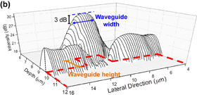
Download figure:
Standard image High-resolution image
Fig. 3. (a) Depth profile curves obtained at RWG (black line) and substrate (red line). (b) Summarized profile curves. (c) OCT image and (d) Cross-sectional SEM image of the 3-µm-wide RWG.
Download figure:
Standard image High-resolution imageWe obtained the depth profile curves by scanning with the light probe at intervals of 0.2 µm in the lateral direction across the RWG and summarized the profile curves in Fig. 3(b). The reflection peaks at the surfaces of the substrate and the RWG can be clearly distinguished. Based on the depth profile curves, signal intensity was scaled on an 8-bit gray-scale where white denotes maximum and black denotes minimum, and a cross-sectional OCT image was constructed, as shown in Fig. 3(c). The surface line of the substrate and the RWG indicated by a red dashed line was determined at the reflection peak position. At the boundary between the RWG and the substrate, the incident light probe spanned both the surfaces and the signal intensities were overlapped in a short range of the lateral direction; thus, we define the boundary position where the peak intensity dropped 3 dB from the peak intensity of the RWG surface. The estimated RWG height and width from the OCT image were approximately 1.52 and 2.25 µm, respectively. These values correspond well with the values measured through SEM observation — 1.52 and 2.20 µm, respectively, as shown in Fig. 3(d). As compared with our previous data obtained with conventional achromatic lenses,28) the clearness of imaging was improved, in particular, at the boundary of the RWG and the substrate. This is caused by reduction of the intensity overlap at the boundary, resulting from the reduced spot size (lateral resolution) using the high NA objective lens. Considering that the conventional achromatic lenses even with high NA were not able to reduce the spot size while maintaining the axial resolution less than 1 µm, the aberration of the lens might affect the axial resolution; thus, the plan apochromatic aberration correction can be effective for obtaining a high lateral resolution compatible with the high axial resolution.
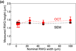
In the same manner, we measured the height and width of the fabricated RWGs with various nominal widths by vis-OCT and SEM, as summarized in Table I. Figures 4(a) and 4(b) show the comparison of the measured height and width of various RWGs between vis-OCT and SEM. While the SEM measurements were performed only for a cleaved edge of each RWG, the vis-OCT measurements were performed on five different positions of each RWG, and their average and standard deviation values are indicated in the figure by points and error bars, respectively. The measured height values shown in Fig. 4(a) were almost the same as that of the nominal etching depth — 1.5 µm, independent of the RWG width, and the measured height values were similar between the vis-OCT and SEM. The vis-OCT measurement is a non-destructive measurement method; thus, measurements at multiple positions can be performed, whereas, for the SEM measurement, it is necessary to cleave the sample and conducting multiple measurements is difficult. The statistical result obtained from multiple measurements with vis-OCT should be beneficial to determine precise values. Moreover, the measured RWG widths shown in Fig. 4(b) were almost same as the nominal width. The standard deviations of the width measured using vis-OCT were exceptionally small (0.4–0.7 µm, as shown in Table I) as compared to the scale of the graph, and hence the error bars were omitted. The black solid line indicates where the nominal width corresponds to the measured width. The widths measured by vis-OCT and SEM were also similar. These results demonstrate that vis-OCT is available for precise measurement of the height and width of the semiconductor RWGs.
Table I. Measured height and width values using vis-OCT and SEM.
| Nominal RWG width (µm) | Average value of measured RWG height by vis-OCT (µm) | Standard deviation of measured RWG height by vis-OCT (µm) | Measured RWG height by SEM (µm) | Average value of measured RWG width by vis-OCT (µm) | Standard deviation of measured RWG width by vis-OCT (µm) | Measured RWG width by SEM (µm) |
|---|---|---|---|---|---|---|
| 3 | 1.49 | ±0.08 | 1.52 | 2.25 | ±0.26 | 2.20 |
| 5 | 1.50 | ±0.09 | 1.52 | 4.49 | ±0.20 | 4.42 |
| 25 | 1.58 | ±0.08 | 1.52 | 24.7 | ±0.36 | 25.2 |
| 50 | 1.53 | ±0.06 | 1.50 | 48.3 | ±0.25 | 49.6 |
| 100 | 1.59 | ±0.08 | 1.53 | 97.8 | ±0.30 | 102 |
Download figure:
Standard image High-resolution image
Fig. 4. Comparisons between the measured values of vis-OCT and SEM (a) RWG height and (b) RWG width.
Download figure:
Standard image High-resolution image
Based on the above results, we demonstrated that vis-OCT enables non-destructive and high-resolution cross-sectional measurement of the RWG formed on the substrate surface. We consider that vis-OCT can also be utilized to measure buried-type optical waveguides, such as Si strip waveguide covered with a relatively low refractive index material, SiO2 (n = 1.5 for visible broadband light),29) which are frequently used for silicon photonics technology.30,31) The SiO2 layer is transparent for visible light, and the reflective index difference between Si and SiO2 is large; thus, the reflection at the boundary of the buried waveguide can be detected. In addition, the axial resolution can be smaller than that in air because the axial resolution is inversely proportional to the refractive index according to Eq. (1). With regard to the lateral resolution, a value of approximately 500 nm should be required because the typical width of Si strip waveguide used for Si photonics technology is less than 600 nm. For a buried type Si waveguide, in the same manner as the axial resolution, the lateral resolution may be reduced to the value of the spot size in air divided by the refractive index of SiO2 (n = 1.5), i.e., approximately 450 nm. In addition, for an exposed Si waveguide, identical reduction of the lateral resolution can be achieved by immersion of the lens in a high refractive index oil, corresponding to the SiO2. Thus, although further investigation is necessary, vis-OCT can be expected to find applications for even smaller optical waveguides in Si photonics technology.
4. Conclusions
We demonstrated non-destructive and non-contact inspection for semiconductor RWGs using vis-OCT with high axial and lateral resolutions of less than 1 µm. Cross-sectional OCT images of the RWGs were obtained, and the height and width of the RWGs were measured. The measured height and width values were similar to those measured by SEM. These results indicated the effectiveness of vis-OCT for inspection of semiconductor optical waveguides without destruction and contact processes.
Acknowledgments
This work was partly supported by the Matching Planner Program sponsored by the Japan Science and Technology Agency (JST), and Ushio Inc. The RWG sample fabrications were supported by the NIMS Nanofabrication Platform in the "Nanotechnology Platform Project" sponsored by the Ministry of Education, Culture, Sports, Science and Technology, Japan (MEXT).