

Abstract
Analysis on the temperature-dependent Raman spectra measured between 27–450 °C range in relation to various Ge compositional ratios of Cu2Sn1−xGexS3 thin-film alloys, which were prepared by closed-tube sulfurization technique, was carried out in detail. By XRD and Raman analyses, linear transformation of the lattice parameters for Cu2Sn1−xGexS3 thin-film alloys with respect to the Ge composition was confirmed to be obeying the Vegard's law. By AC Hall effect measurement, reducing of carrier mobility was observed in the Cu2Sn1−xGexS3 thin-film alloys with higher Ge content. By the temperature dependent Raman spectroscopy analysis, it is observed that the red shifting of Raman vibration energy due to the thermal expansion is resembled to that of the temperature dependency of energy bandgap of semiconductors. Anisotropic thermal dilatation behavior was observed in the Cu2Sn1−xGexS3 thin-film alloy independent of its Ge composition.
Export citation and abstract BibTeX RIS
1. Introduction
Nowadays, Cu2Sn1−xGexS3 (0 ≤ x ≤ 1) (CTGS) multinary compound is recognized as one of the new alternative solar absorber materials for the thin-film photovoltaic applications due to its properties such as low toxicity, high absorption coefficient (>104 cm−1), chemical stability, and availableness of various bandgaps between 0.94–1.3 eV, which are in good matching to the solar spectrum of high energy density range by adjusting the compositional ratio of Ge and Sn.1–10) Recently, the photovoltaic cells based on the CTGS absorbers exhibited a power conversion efficiency over 6%, which is an impressive achievement.10) By optimizing the characteristic of CTGS absorbers as well as device structure, efficiency over 25% is expectable in the future according to the detailed balance theory.11) However, the study of CTGS compound is still immature and reports concerning to this compound are relatively few compared to the well-developed absorber materials such as Si, GaAs, Cu(In,Ga)Se2, CdTe, and Cu2ZnSn(S,Se)4.1–10,12–17) Besides, formation of different crystal phases as well as unintended secondary phases is one of the major problems for this material system due to its multinary elemental composition.18–28) Hence, it is important to explore the material properties relating to its impurity phases as well as fabrication techniques of CTGS multinary compound by various theoretical and experimental approaches in order to improve its characteristics. Temperature-dependent Raman analysis has advantages over the conventional room temperature measurement in understanding the different behavior of secondary phases mixed unintentionally in the CTGS. This technique was already reported for the other material systems such as Si and Cu2ZnSn(S,Se)4, however, still remained unexplored for the CTGS.29–33) Based on the combining analyses of X-ray diffractometry (XRD) and Raman spectroscopy, we previously reported the formation of different crystalline phases of CTGS thin-film alloys prepared at various temperatures under a closed-tube sulfurization process utilizing laminated precursors.5) We also indicated the fluctuation of photovoltaic characteristics caused by variation of crystalline properties of the CTGS absorbers. In this paper, we focused on the behavior of Raman scattering for each vibration mode observed in the CTGS thin-film alloys under various lattice temperatures in order to clarify their crystalline properties for the first time.
2. Experimental methods
The CTGS thin-film alloys were prepared on the Mo coated soda-lime glass (SLG; Matsunami S7213) substrates by a closed-tube sulfurization of Cu/Ge/Sn laminated precursors at the temperatures above 550 °C under sulfur pressure of 1 atm. To suppress re-evaporation of Ge during sulfurization process, a suitable mount of GeS was enclosed in the ampoule together. The compositional ratios of the thin films were controlled by adjusting the thickness ratios of the individual elements such as Cu, Sn, and Ge. The Cu/[2(Ge + Sn)] ratio of the samples utilized in analyzing the effect of Ge content was adjusted near the stoichiometric value of 1.00 ± 0.05. The details of thin films preparation process and sulfurization technique were reported elsewhere.5,34,35) The actual chemical compositions of the samples utilized in this experiment were described in Table I. An XDR (Rigaku RINT-2200V/PCSV, Cu Kα ray, λ = 1.5418 Å with a Bragg–Brentano θ–2θ geometry at 40 kV, 30 mA) was used to identify the crystalline quality of the thin films. The surface morphology of the thin films was observed by a field emission scanning electron microscope (FE-SEM; Hitachi S-4100). An electron probe microanalysis (EPMA; Shimadzu EPMA-1610) was used to measure the final chemical composition of the CTGS thin-film alloys. The electrical properties of square-shape (6 mm2) thin films deposited directly on SLG substrates were evaluated by utilizing an AC Hall effect measurement system (Toyo Technica 8400A CLR/OW). Pt electrodes were used to achieve good ohmic contact with the CTGS thin films during the Hall effect measurements. For the Raman spectroscopy analyses, a laser Raman spectrometer (COMET-3504) equipped with an Nd:YVO4 second-harmonic generation (SHG) laser (continuous wave of λ = 532.3 ± 0.3 nm and maximum power of 500 mW) and a monochromator (SOL Instruments MS-35041) was used. The spectral resolutions of the system are 0.06 and 0.045 nm for the grating of 1800 and 2400 lines/mm, respectively. The measurement spectra were obtained in the backscattering geometry and were captured by a CCD detector (ANDOR iDUS DU420A-BR-DD, pixel size of 14 µm). During the temperature-dependent Raman spectroscopy measurement, the sample to be measured was set in a crucible made of platinum, which is placed inside a vacuum chamber to avoid unintended reaction with the ambient at high measurement temperatures. The temperature of the sample (27–450 °C) was adjusted by a feedback-controlled heating system with precision of ±1.0 °C. For high-lattice-temperature measurements, the acquisition of Raman spectra was carried out after keeping adequate period to achieve steady equilibrium state at the specific lattice temperature so that transient effect due to the temperature alteration can be avoided.
Table I. Comparison of chemical compositions of the CTGS thin films with various x = Ge/(Ge + Sn) ratios (in %).
| x | Cu | Ge | Sn | S |
|---|---|---|---|---|
| 0.00 | 30.0 | 0.0 | 14.7 | 55.4 |
| 0.20 | 30.2 | 3.1 | 12.2 | 54.5 |
| 0.45 | 29.4 | 7.0 | 8.6 | 55.1 |
| 0.67 | 30.4 | 10.1 | 5.0 | 54.4 |
| 0.82 | 29.1 | 13.1 | 2.9 | 54.8 |
3. Results and discussion
The XRD patterns of the samples with different Ge compositions are shown in Fig. 1. The peaks observed near 40.5 and 58.6° are due to the Mo substrate. A prominent peak, which is attributed to  plane diffraction of monoclinic, is detected around 28.4° for the sample without Ge content. Weak peaks around 16, 18, and 21°, which are belonging to (110),
  , and (021) diffractions of monoclinic phase, are also clearly observed in the samples with x = 0.20–0.67. Peak shifting towards higher diffraction angle was observed for all the samples with larger Ge contents. This result indicates the lattice shrinkage due to the substitution of smaller Ge atom into the larger Sn site in the host crystal lattice. Other peaks due to impurity phases are not detected. The details of lattice parameters of the monoclinic phase of the CTGS thin-film alloys with various Ge/(Ge + Sn) = x ratios deducted from the corresponding lattice spacing of XRD measurement results are shown in Fig. 2. The calculation of lattice parameters was done by utilizing Eq. (1) showing the crystal geometry relationship between the Miller indices
  and the corresponding lattice spacing (d) in terms of the lattice parameters such as a, b, c, α, β, and γ of monoclinic crystal.
It is observed that the lattice parameters of the sample with x = 0.00 are a = 6.65 Å, b = 11.52 Å, and c = 6.64 Å, which are decreased proportionally with increasing of the Ge/(Ge + Sn) ratio. For the sample with x = 1.00, it is observed to be a = 6.47 Å, b = 11.28 Å, and c = 6.41 Å, respectively. The lattice angles for the sample with x = 0.00 (1.00) are α = 90° (90°), β = 109.4° (108.34°), and γ = 90° (90°), respectively. Hence, the larger the Ge/(Ge + Sn) ratio, the smaller is the fundamental lattice constants a, b, and c of monoclinic phase, which exhibits good agreement to the approximation (the straight dash-lines depicted in Fig. 2) by Vegard's law using the following equation.36,37)

Here, A(x) is the corresponding lattice parameters such as a, b, or c depending on the Ge content of x. ACGS and ACTS represent the lattice parameters at x = 1.00 and 0.00, respectively. For ACGS and ACTS, the parameters of ICDD-01-088-0827 and ICDD-01-070-6338 XRD patterns were used in the calculation.

Fig. 1. XRD patterns of CTGS thin films with various x = Ge/(Ge + Sn) ratios.
Download figure:
Standard image High-resolution image
Fig. 2. The lattice constants a, b, and c of the CTGS thin films with various Ge/(Ge + Sn) ratios deduced from the XRD patterns using Eq. (1). The dash-lines indicate the approximations by Vegard's law using Eq. (2) for the corresponding lattice constants of the monoclinic phase.
Download figure:
Standard image High-resolution imageThe surface morphology of the samples with various Ge compositions is shown in Fig. 3. It is observed that the average crystal grain size of Ge incorporated samples is relatively larger than the sample without Ge content. Crystal grains larger than 1 µm, which is over 2 times greater than the samples without Ge, are achieved in the samples with x = 0.20 and 0.45 as shown in Figs. 3(b) and 3(c). However, the enhancement of crystalline size is not obvious for the samples with x = 0.67, 0.82, and 1.00 as shown in Figs. 3(d)–3(f). It is also observed that the films with Ge contents higher than x = 0.45 are relatively brittle and easy to peel off from the substrate. Poor correlation of Ge content could be due to the existence of other additional factors, which are effecting the growth of crystal grain as well as that of the apparent surface morphology. The Hall effect measurement results of the samples with x = 0.00, 0.20, 0.45, and 0.67 are compared in Table II. All the samples exhibit p-type conductivity. The resistivity is increased from 2.6 × 10⁻¹ to 1.8 × 101 Ω cm as the Ge content increased to x = 0.45. However, it is lower to about 2.9 × 100 Ω cm in the sample with x = 0.67. On the other hand, Hall mobility and carrier concentration are reduced in the samples containing Ge, although larger crystal gain size was achieved in the samples with x = 0.20 and 0.45 compared to the one without Ge. The decreasing of carrier concentration could be due to lower defect density and/or increasing of bandgap by Ge incorporation in the lattice.5) However, the reducing of Hall mobility could be due to the existence of irregular grain boundaries, secondary phases and/or larger alloy scattering in the samples with higher Ge content.38) Additionally, such deviations could also be the reason of low correlation between this Hall effect measurement result to that of the apparent surface morphology discussed above.

Fig. 3. SEM images of the surface of CTGS thin films with (a) x = 0.00, (b) x = 0.20, (c) x = 0.45, (d) x = 0.67, (e) x = 0.82, and (f) x = 1.00, respectively.
Download figure:
Standard image High-resolution imageTable II. Comparison of AC Hall effect measurement results of the CTGS thin films with various Ge compositions.
| x = 0.00 | x = 0.20 | x = 0.45 | x = 0.67 | |
|---|---|---|---|---|
| Resistivity (Ω cm) | 2.6 × 10⁻¹ | 9.6 × 100 | 1.8 × 101 | 2.9 × 100 |
| Hall mobility (cm2 V−1 s−1) | 6.9 × 10⁻¹ | 5.6 × 10⁻¹ | 3.1 × 10⁻¹ | 2.7 × 10⁻¹ |
| Carrier type | p | p | p | p |
| Carrier concentration (cm−3) | 3.8 × 10¹⁹ | 1.2 × 10¹⁸ | 1.1 × 10¹⁸ | 8.0 × 10¹⁸ |
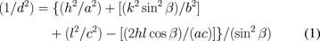
The temperature-dependent Raman spectra of the sample without Ge substitution are shown in Fig. 4(a). During the measurements, the sample temperature was increased from 27 °C (room temperature) to 450 °C by 50 °C increment. The spectrum of room temperature is depicted at the bottom and those of higher temperatures are described toward the top of the graph as shown in Figs. 4(a)–4(e). For the sample without Ge incorporation, two prominent peaks, denoted as "a1" and "a3", are observed at 304 and 361 cm−1 along with weaker and broader peaks, described as "a2" and "a4", on their corresponding right hand side at room temperature (27 °C), respectively. The peaks a1 and a3 are attributed to main A' mode vibration of monoclinic phase.19,39–41) Besides, a broad spectrum around 280 cm−1, which corresponds to the Cu2Sn3S7 phase, is also detected.5,6,42) The relative intensity of a3 is reducing faster than that of a1 when the temperature is increased. The broadening of full width at half maximum (FWHM) of each peak are also observed. The higher the lattice temperature, the broader is the peak. This clearly indicates the increasing of thermal disordering of crystal lattice at higher temperatures. The peak shifting toward lower vibration sides due to the thermal dilatation of the lattice for all these peaks is also observed at higher temperatures.
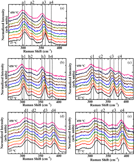
Fig. 4. Temperature-dependent Raman spectra of the samples with (a) x = 0.00, (b) x = 0.20, (c) x = 0.45, (d) x = 0.67, and (e) x = 0.82. The spectrum obtained at 27 °C is plotted at the bottom. The spectra measured at higher temperatures up to 450 °C are plotted upward with 50 °C increment. Base-line offset is done for visual enhancement.
Download figure:
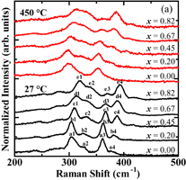
Standard image High-resolution imageThe temperature-dependent Raman spectra of the samples with Ge contents of x = 0.20, 0.45, 0.67, and 0.82 are shown in Figs. 4(b)–4(e), respectively. Two main vibration peaks, denoted as "X1" and "X3" (where the notation "X" represents either a or b or c or d or e for the corresponding sample), which are attributed to A' mode vibrations of monoclinic crystal similar to that of peaks a1 and a3 of the sample with x = 0.0, are also observed at higher vibrations, respectively. Another two main peaks, described as "X2" and "X4", are also detected at the corresponding right side of "X1" and "X3", respectively. The relative intensity of "X2" and "X4" peaks are stronger in the samples with higher Ge contents at both 27 and 450 °C as compared in Fig. 5(a). Since these two vibration modes are favor in the Ge dominant lattice, their origin could be attributed to the vibration of Ge atoms with respect to the sulfur anions.5) However, the relative intensity of X3 is reduced, while that of X1 is remained the same when the composition of Ge is higher independent of the sample temperature. In addition, linear dependency for all the vibration modes (X1, X2, X3, and X4) to the Ge content is also found as shown in Fig. 5(b). This result is consistent with that of the XRD analysis discussed above. The peak broadening due to the sample temperature for all vibration modes for these samples are also observed. The higher the sample temperature, the wider is the FWHM of the corresponding peak. As the temperature of the samples is increased, the positions of all these peaks are shifted towards weaker vibration sides (red shifting) compared to their corresponding peak at lower temperature, which is similar to that of the sample without Ge. These results indicate a clear evidence of thermal dilatation behavior in the CTGS alloy, which directly effects on the change in energy of optically coupled vibrations such as Raman active modes of the lattice. Similarly, bandgap narrowing effect due to this thermal expansion of the lattice as explain by Varshni is also expectable in this CTGS alloy.43) In other words, a similar tendency of change in the Raman red shifting along with the bandgap narrowing phenomenon due to the increasing of lattice temperature could be observable, although the absolute quantity of energy involved in the two processes could be totally different.
Download figure:
Standard image High-resolution image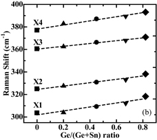
Fig. 5. (a) A comparison between the Raman spectra measured at 27 °C (spectra with black lines shown at the lower part) and 450 °C (spectra with red lines shown at the upper part) for the samples with various Ge compositions. (b) The Raman peak shifting of the individual X1, X2, X3, and X4 with respect to the Ge composition of the CTGS thin films at 27 °C.
Download figure:
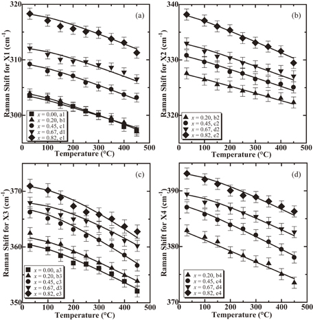
Standard image High-resolution imageTo investigate the temperature dependent behavior in detail, peak separation and fitting for each spectrum were carried out. By assuming the form of individual peak that composing the Raman spectrum as Gaussian distribution for each, the position of prominent peaks X1, X2, X3, and X4 for each sample are identified at each temperature. The detailed amount of Raman shifting due to the sample temperature for each peak is described in Figs. 6(a)–6(d). For peaks a1 and a3 of the sample without Ge at 450 °C, the vibrations are reduced to about 6 and 9 cm−1, respectively, compared to that of the corresponding peak at room temperature. It is observed that the changes of vibration energy (νT) for these peaks due to the lattice temperature exhibit a good agreement to the following expression as expected:

which is similar to the temperature dependency of energy bandgap of semiconductors as explained by Varshni.43) Here, νo stands for vibration energy at room temperature, φ and ζ are material dependent constants, and T is a lattice temperature. The fitting lines based on Eq. (3) are depicted as solid lines in the corresponding plots of the graphs shown in Figs. 6(a)–6(d). The fitting values of φ and ζ for a1 (a3) are 1.5 × 10⁻² (2.5 × 10⁻²) cm−1/°C and 7.6 × 101 (1.5 × 10²) °C, respectively, for the sample without Ge. Since the amount of changes is different for different vibration modes, this could be the indication of either anisotropic thermal expansion behavior of monoclinic lattice or the existence of different crystalline phases such as cubic or tetragonal with different thermal expansion property due to the temperature. The fitting values of φ and ζ for e1 (e3) are increased to 2.1 × 10⁻² (4.2 × 10⁻²) cm−1/°C and 2.1 × 10² (4.5 × 10²) °C, respectively for the sample with x = 0.82. The detailed of the fitting values for individual peak is summarized in Table III. The higher Ge incorporation in the CTGS lattice, the larger are φ and ζ values, except a few deviation in the samples with x = 0.67. This result indicates that thermal expansion rate of CTGS alloys is larger at higher Ge composition. In comparing the same X1 vibration mode of the samples with different Ge compositions as shown in Fig. 6(a) in detail, it is observed that the trends of temperature dependency of the samples with x = 0.00 (a1) and x = 0.20 (b1) are almost the same, while those of x = 0.45 (c1), x = 0.67 (d1), and x = 0.82 (e1) also exhibit similar curvature, however, at different vibrations. In addition, the accuracy of fitting (shown as solid lines in Fig. 6) calculated by Eq. (3) is relatively low in the samples with x = 0.67 (d1) and x = 0.82 (e1), which could be due to the existence of either localized phases with different Ge compositions or different crystalline forms in those samples. In the case of X2 mode as shown in Fig. 6(b), temperature dependency with smaller curvature compared to X1 is observed in the peak b2, c2, d2, and e2, except that of a2 which is too weak to be confirmed clearly. For X3 mode, the variation trends for a3, b3, c3, d3, and e3 are much resemble to those of X1, however, with larger curvature as shown in Fig. 6(c). On the other hand, the temperature dependency of X4 mode of peaks b4, c4, d4, and e4 is similar to that of X2 as shown in Fig. 6(d). Intuitively, the behavior of thermal dependency of X1 and X3 modes could be categorized in one group, while that of X2 and X4 modes to another group since X1 (X2) and X3 (X4) have similarity in the curvature of temperature dependency. In comparison, the influence of Ge composition on the temperature-dependent curvature is relatively small, while the difference in the curvature between the individual vibration modes is obvious. This change in the curvature between the vibration modes could be the indication of anisotropic thermal dependent characteristic such as anharmonic effect of the CTGS alloy independent of its Ge composition.
Fig. 6. Variation of Raman shift due to the temperature for individual (a) X1, (b) X2, (c) X3, and (d) X4 peak of the samples with various Ge compositions. Solid lines describe the fitting lines expected by Eq. (3).
Download figure:
Standard image High-resolution image
Table III. Comparison of fitting parameters φ (cm−1/°C) and ζ (°C) calculated by Eq. (3) for each vibration modes of CTGS thin films with various Ge compositions.
| Vibration peaks | Fitting parameters | ||
|---|---|---|---|
| φ | ζ | ||
| X1 | a1 | 1.5 × 10⁻² | 7.6 × 101 |
| b1 | 1.8 × 10⁻² | 1.1 × 10² | |
| c1 | 1.9 × 10⁻² | 1.4 × 10² | |
| d1 | 1.9 × 10⁻² | 2.0 × 10² | |
| e1 | 2.1 × 10⁻² | 2.1 × 10² | |
| X2 | b2 | 1.3 × 10⁻² | 2.8 × 101 |
| c2 | 1.6 × 10⁻² | 5.1 × 101 | |
| d2 | 1.7 × 10⁻² | 7.1 × 101 | |
| e2 | 2.0 × 10⁻² | 7.3 × 101 | |
| X3 | a3 | 2.5 × 10⁻² | 1.5 × 10² |
| b3 | 2.6 × 10⁻² | 2.2 × 10² | |
| c3 | 3.3 × 10⁻² | 2.4 × 10² | |
| d3 | 3.4 × 10⁻² | 4.6 × 10² | |
| e3 | 4.2 × 10⁻² | 4.5 × 10² | |
| X4 | b4 | 2.0 × 10⁻² | 1.7 × 101 |
| c4 | 2.4 × 10⁻² | 8.0 × 101 | |
| d4 | 2.4 × 10⁻² | 2.0 × 10² | |
| e4 | 2.5 × 10⁻² | 2.2 × 10² | |
Note: a1 and a3 represent the spectra of sample with x = 0.00. b1, b2, b3, and b4 depict the spectra of sample with x = 0.20. c1, c2, c3, and c4 describe the spectra of sample with x = 0.45. d1, d2, d3, and d4 stand for the spectra of sample with x = 0.67. e1, e2, e3, and e4 show the spectra of sample with x = 0.82, respectively.
4. Conclusions
A detailed analysis on the temperature-dependent Raman spectroscopy measured between 27–450 °C range in relation to various Ge compositional ratios of Cu2Sn1−xGexS3 thin-film alloys, which were prepared by closed-tube sulfurization technique, were carried out. It was observed that the lattice parameters of the sample without Ge incorporation are a = 6.65 Å, b = 11.52 Å, and c = 6.64 Å, which are decreased proportionally with increasing of the Ge/(Ge + Sn) ratio obeying the Vegard's law. Reducing of carrier mobility in the Cu2Sn1−xGexS3 thin-film alloys with higher Ge content was observed by AC Hall effect measurement. The red shifting of Raman peaks due to the thermal dilatation behavior of Cu2Sn1−xGexS3 thin-film alloy independent of its Ge composition was confirmed. Anisotropic alteration of Raman vibration energy due to the thermal expansion is similar to that of the temperature dependency of energy bandgap of semiconductors.
Acknowledgment
The authors would like to thank Mr. Isamu Minemura for his great help in setting up the experimental equipments.