

Abstract
A multi-quantum-shell (MQS) grown on a GaN nanowire is a promising three-dimensional active region and it is expected to show excellent performance, compared with conventional nitride-based LEDs. However, there are no suitable simulators for calculating optical properties of MQS-LEDs, because of their complex structure. In this study, a hybrid simulation, which is composed of the finite-difference time-domain method, the rigorous coupled wave analysis method, and the ray tracing method, is developed. Applying this useful tool to the calculation of the light extraction efficiency (LEE) of MQS-LEDs, we have found considerable light absorption loss by the large refractive index steps between the active layer, ITO layer and air in the commonly used MQS-LED structure with the ITO electrode. Thus, to eliminate the large refractive index steps, the MQS-LED buried with the n-GaN current diffusion layer, which has a high LEE, was proposed.
Export citation and abstract BibTeX RIS
1. Introduction
Over the last two decades, the performance of group-III nitride-based LEDs has been significantly improved,1–2) and they have been used in many applications such as general lighting sources, liquid crystal displays and automobile headlights. All the commercially available nitride-based LEDs include the multi-quantum well (MQW) active layer,3) which is a kind of two-dimensional structure. And they exhibit very high quantum efficiency,4,5) in particular in the violet to blue color range. However, there are still remains problems, for instance, efficiency droop6–9) and green-gap.6,10–11)
Under such current situations surrounding the nitride-based LEDs, GaN nanowires (NWs) have been the focus,12–15) as a new three-dimensional platform of nitride-based photonic devices. The NW is a hexagonal columnar crystal, and our interest is toward the vertical direction by the selective area growth (SAG) technique.13,16–21) Many SAG-NWs reported in the literatures have a submicron-order diameter and micron-order height, although the size varies depending on research group. Among them, the multi-quantum shell (MQS)/NW structure is expected to have excellent optical properties because it grows in the active region on the nonpolar m-plane, which leads to the absence of quantum confined Stark effect.22–24) As another advantage of NWs, reduction or elimination of defects is expected.25,26) Furthermore, MQS grown on the nonpolar plane are considered to solve the green-gap problem, because the causes of this problem are believed to be the high-density defect and increase of the piezoelectric polarization in the long wavelength LED, and the MQS could solve them as mentioned above.
Although theoretical analysis is important in designing semiconductor devices, the MQS-LEDs had no suitable simulation tools due to their complicated structure. For example, since the NW is a submicron-order periodic light emitting element, the influence of the wave nature of light cannot be ignored, but the ray tracing (RT) method, which is a widely used simulation method in LEDs, does not take into account the wave nature of light, so that it is not appropriate. In other words, calculated results in MQS devices by the RT method are theoretically incorrect. Although the finite-difference time-domain (FDTD) method is versatile in most device simulations, it takes a huge amount of time to calculate a complex and periodic structure model such as NWs, and it is not a practical means. Then, in this study, by combining several simulation methods, we established a hybrid simulation method considering the wave nature of light in a realistic calculation time. Then we analyzed optical properties such as the light extraction efficiency (LEE) of MQS-LEDs. As a result, it was found that in the MQS-LED, the light absorption in the layer with the absorption coefficient such as the electrode and the active layer have a large influence on the optical characteristics, and, by replacing the absorptive ITO electrode with the no absorbing n-GaN current diffusion layer, a considerably high LEE is predicted in our simulation. Furthermore, as a device structure with higher LEE, we propose a textured surface on the n-GaN current diffusion layer in the MQS-LEDs.
2. Simulation method for MQS-LED
In our study, we have established our original simulation technique for calculating the LEE of MQS-LED, which is composed of three kinds of theoretical approaches; the FDTD method,27,28) the rigorous coupled wave analysis (RCWA) method29) and the RT method. In the FDTD method, we obtained the radiation property of a single MQS active region. Then, we analyzed the dispersion characteristics such as an angle distribution of the transmittance and reflectance from the periodic arrangement of MQS/NWs by the RCWA method. Finally, the light extraction efficiency of MQS-LED was calculated by the RT method, where the radiation property obtained by the FDTD method was set as the light source, and dispersion characteristic from the RCWA method was referred at the surface of the LED. In this system, the RT method (particle calculation theory) is applied for almost all the 3D-LED structure, except the surface. When the photons reach the surface in the RT calculation, the data of the angle distribution of the transmittance and reflectance by RCWA method are taken. Therefore, a calculation time could be considerably saved, and it is possible to reasonably reproduce the MQS-LED operation. A configuration of the simulation procedure is shown in Fig. 1. The simulation is carried out in a 3D model in all processes. In order to save calculation time of the simulation, the shape of the NWs, which is actually a hexagonal rod, is approximated to be a cylindrical rod. The physical parameters used in this study are listed in Table I.
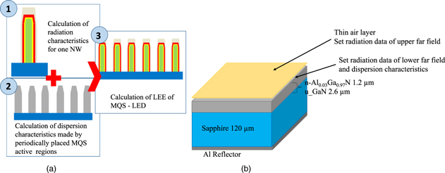
Fig. 1. (Color online) (a) Configuration of the simulation method, and (b) schematic simulation model. In (a) the NW, which is actually a hexagonal pillar, is approximated to be a cylinder. This approximation may be allowed, because of the in-plane (c-plane) symmetry of electronic structures and light emission probability of hexagonal nitride semiconductors.
Download figure:
Standard image High-resolution imageTable I. The physical parameters used this study.38,39)
| Parameter | Value |
|---|---|
| Al | n = 0.5025 κ = 4.920 |
| sapphire | n = 1.78 κ = 0.0 |
| u-GaN | n = 2.555 κ = 0.0 |
| n-Al0.03Ga0.97N | n = 2.530 κ = 0.0 |
| n-GaN | n = 2.555 κ = 0.0 |
| MQS (the average composition) | n = 2.631 κ = 3.223E-03 |
| p-GaN | n = 2.555 κ = 3.223E-04 |
| ITO | n = 2.28 κ = 0.018 |
| the emission wavelength [nm] | 405 |
| the thickness of sapphire substrate [μm] | 120 |
| the thickness of u-GaN template [μm] | 2.6 |
| the thickness of n-AlGaN template [μm] | 1.2 |
| the height of NW [μm] | 1.5 |
| the diameter of n-GaN core-NW [nm] | 200 |
| the thickness of MQW [nm] | 37 |
| the thickness of p-GaN [nm] | 100 |
| the thickness of ITO of side [nm] | 60 |
| the thickness of ITO of top [nm] | 400 |
| the thickness of n-GaN current spreading layer from top of NW [nm] | 500 |
As MQS-LED structures for the calculation of the LEE, we produced various kinds of device structure models shown in Figs. 2–4. The MQS-LED with a ITO semi-transparent electrode shown in Fig. 2 is quite a common structure for this kind of device,12–15,30) however, the LEE of this device is not so high, as mentioned later. As in our original design, the MQS-LED with an n-GaN current diffusion layer, where all the MQSs are buried by the n-GaN current diffusion layer to planarize the surface of the devices, and a p++-GaN/n++-GaN tunnel junction31–34) is induced between the MQS and the n-GaN current diffusion layer to enable the current flow, is quite promising for uniform current injection to m-plane MQS active regions35,36) and also high LEE. Therefore, we also calculated some variations of the MQS-LEDs with the n-GaN current diffusion layer shown in Figs. 3 and 4. Among the LED structural components, ITO, MQS and p-GaN have a non-zero optical absorption coefficient, and they considerably influence the LEE, as discussed later. In all LEDs, light is extracted from the epilayer-side, and the Al reflector was placed on the backside of the sapphire substrate. All the LEE calculations in this study are those from the inside of the LED to the air without resin encapsulation.
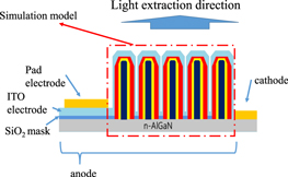
Fig. 2. (Color online) Schematic diagram of MQS-LED with ITO electrode.
Download figure:
Standard image High-resolution image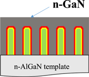
Fig. 3. (Color online) Schematic diagram of MQS-LED with n-GaN current diffusion layer.
Download figure:
Standard image High-resolution image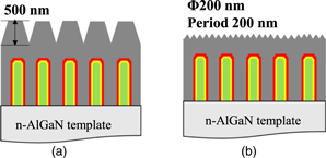
Fig. 4. (Color online) Schematic diagrams of MQS-LED; (a) surface texture with long pitch, and (b) that with short pitch.
Download figure:
Standard image High-resolution image3. Results and discussion
3.1. Conventional LED with planar MQW active layer
As a reference of the MQS-LED, the LEE of the conventional planar blue LED, which equips the ITO semi-transparent electrode and a patterned sapphire substrate (PSS), is taken, since many researchers in the field of LEDs already know experimentally and theoretically. Based on this LED structure, the highest external quantum efficiency ever reported is 84.3%.37) Since this value is obtained only at a low current density, where the internal quantum efficiency is almost equal to 100%, the external quantum efficiency can be regarded as the LEE. Since the highest LEE37) was taken for the device with a resin encapsulation, the LEE toward the air is estimated to be around 60%. This value is a reference to those of the MQS-LEDs.
3.2. MQS-LED with semi-transparent ITO electrode
As mentioned above, the MQS-LED covered with a semi-transparent ITO electrode is a simple and common LED structure with NWs.7–10,13) We firstly applied our new calculation system described in Sect. 2 to this device for the calculation of the LEE. The results of the LEE calculation for this device and the referenced planar LED are shown in Table II. Calculated LEE for this type of MQS-LED is obtained to be just 30.6%, which is much lower than that of the conventional planar device. In the device structure, a horizontal arrangement of the air/ITO/MQS/NW includes the large refractive index steps, and they cause the multiple reflections of the light horizontally. During such multiple reflections, a large part of the light might be absorbed in ITO, p-GaN and MQS. Therefore, upward emission was lower than downward emission from the initial light source.
Table II. The calculated LEE for various devices.
| MQS-LED with n-GaN current diffusion layer | ||||
|---|---|---|---|---|
| Planar LED (reference) | MQS-LED with ITO electrode | Flat | Surface texture (long pitch) | Surface texture (short pitch) |
| 0.60 | 0.306 | 0.485 | 0.353 | 0.536 |
They may be quite a surprising result, while many people expect the high LEE in NW-related LED, due to the 3D-texture structure on the surface. Our results greatly suggest that too high refractive index steps in the horizontal direction should be eliminated, in order to realize the high LEE. In the next section, this argument will be proven by the calculation for the MQS-LED structure with a flat surface.
3.3. MQS-LED buried with n-GaN as current diffusion layer
In order to solve the problem of the low LEE in MQS-LED described in Sect.3.2, we propose a new MQS-LED structure, where the MQS arrangement is fully buried with an n-GaN current diffusing layer. This device model has a flat surface, as shown in Fig. 3. Therefore, this device has no horizontal large refractive index steps. This device has another advantage; i.e., uniform current injection to the MQS active region by inserting the tunnel junction between the n-GaN current diffusing layer and the p-GaN shell. In this device, since light absorption of n-GaN is considered to be extremely small, the extinction coefficient of the n-GaN current diffusion layer is set to κ = 0. There is no ITO electrode in this device, because low resistive n-GaN works similar to ITO. In the calculation of the LEEs, we added some variations of the device structure. Next, we adopted surface textures on the surface with two different pitches, as shown in Fig. 4, where (a) a longer pitch of 800 nm and a height of 500 nm (a same pitch as MQS arrangement), and (b) a shorter pitch of 200 nm and a height of 200 nm are used.
The results of the LEE calculation described in this section are also shown in Table II. For the simplest MQS-LED buried with the current diffusion layer, the LEE is 48.5%, which is much better than that of the MQS-LED with ITO. Figure 5 shows the incident angle dependence of reflectance/transmittance for (a) MQS-LED with ITO electrode and (b) MQS-LED buried with the n-GaN current diffusion layer. Although MQS-LED with the ITO electrode can emit the light slightly even though the incident angle exceeding the critical angle of the total internal reflection, the lower emission within the critical angle results in the low LEE, and it may be due to the greater absorption loss, as mentioned above. On the other hand, it can be seen that the MQS-LED buried with the current diffusion layer shows higher emission inside the critical angle. As expected, the elimination of the horizontal large refractive index steps gives lower light absorption loss, and it leads to the high LEE. Also in case of the 200 nm pitch surface textured structure, the LEE is improved up to 53.6% which is higher than the simplest MQS-LED buried with the current diffusion layer. However, in the case of the 800 nm pitch surface textured structure, no improvement of the LEE is observed. Since the pitch of 800 nm is the same as that of the MQS arrangement, no change of the diffraction effect leads to the same LEE.

Fig. 5. (Color online) Calculated reflectance/transmittance as a function of incident angle from the normal direction to the primary plane on which NWs are periodically arranged, for (a) MQS-LED with ITO electrode, and for (b) MQS-LED with n-GaN current diffusion layer.
Download figure:
Standard image High-resolution image
Accordingly, owing to the development of the advanced calculation system, we have found the suitable device structure of MQS-LED with considerably high LEE. In the MQS-LED, the elimination of the horizontal large refractive index steps is proven to be indispensable to realize the high LEE.
4. Conclusions
In this study, an optical simulation system for an MQS-LED, which is composed of the FDTD method, RCWA method and RT method, was developed. This calculation system takes into account the lightwave effect with a wavelength-scale structure, and is applicable to the three-dimensional MQS active region. Applying this useful tool to the calculation of the LEE of MQS-LEDs, we have found the considerable light absorption loss by the horizontal large refractive index steps in the commonly used MQS-LED structure with the ITO electrode. Thus, to eliminate the horizontal large refractive index steps, the MQS-LED buried with the n-GaN current diffusion layer was proposed. Obtained LEE for the best MQS-LED is almost comparable to that of the conventional planar LEDs. With other advantages of the MQS-LEDs such as nonpolar face and no extended defects, the high performance will be demonstrated in the near future.
Acknowledgments
This work was supported by the MEXT Private University Research Branding Project, the MEXT Program for research and development of next-generation semiconductor to realize energy-saving society, JSPS KAKENHI for Scientific Research A [No.15H02019], JSPS KAKENHI for Scientific Research A [No.17H01055], JSPS KAKENHI for Innovative Areas [No.16H06416], and Japan Science and Technology CREST [No. 16815710]. The authors would like to thank Mr. Akifumi Nawata of Scivax Co. for their assistance for the simulation.