


Abstract
Weak localization is studied in two high-quality epitaxial graphene samples grown on silicon-faced 6H-SiC substrates. Following the methodology of Kozikov et al (2010 Phys. Rev. B 82 075424), we measured the temperature dependence of carrier conductivity at zero and low magnetic (B) fields. In both samples, a logarithmic temperature dependence of the carrier conductivity was observed at B = 0 and its amplitude was larger than predicted by a single-particle model, suggesting that electron–electron interaction plays an important role in electron transport in epitaxial graphene films.
Export citation and abstract BibTeX RIS
The ground state of a two-dimensional electron system (2DES) at T = 0 has been researched intensively for many years. In particular, electron transport properties in the presence of electron–electron (e–e) interactions have been at the center of recent research [1]. With the arrival of graphene [2–6], new ground states induced by the combination of e–e interactions and massless Dirac fermions have been proposed4. Indeed, the 2DES in graphene may represent a novel two-dimensional (2D) Fermi liquid with unusual e–e interaction physics. Recent observations of the fractional quantum Hall effect at Landau level filling ν = 1/3 [8–10], many-body originated ν = ± 1 states [11], the e–e interaction-induced shift in the cyclotron resonance measurements [12] and the quantum Hall plateau-to-insulator transition [13] demonstrate that a rich, e–e interaction-induced, many-body physics still waits to be discovered in graphene at high magnetic (B) fields.
In comparison, much less experimental work has been performed to examine e–e interactions at zero and low magnetic fields, in particular in epitaxial graphene films. In a recent study in exfoliated graphene films, Kozikov et al [14] observed that e–e interaction [15–22] plays an important role in the low-temperature conductivity of carriers in graphene in the diffusive regime (or kFl ≫ 1, where kF is the Fermi vector and l the electron mean free path) [23]. Furthermore, the e–e interaction correction is sensitive to the details of disorder [14]. It is known that disorder configurations are different in graphene films prepared by different techniques, e.g. exfoliation versus epitaxial growth. Therefore, it is important to experimentally study the interplay between the e–e interaction and disorder and how e–e interaction correction affects the carrier conductivity in epitaxial graphene films.
In this paper, we follow the methodology developed by Kozikov et al [14] and study the e–e interaction in epitaxially grown graphene, through a systematic study of the weak-localization (WL) phenomenon at zero and low B fields. Our results show that the e–e interaction in our epitaxial graphene films also plays an important role in carrier conductivity. Furthermore, the details of the e–e interaction correction term appear to be different in our epitaxial graphene.
The measurements are carried out in two high-quality epitaxial graphene films grown on the silicon-faced 6H-SiC substrates using a method similar to that reported in [24, 25]. Conventional photolithographic techniques were used to fabricate the Hall bar structures of size 50 × 6.25 μm2. The conventional low-frequency phase lock-in technique was used for low-temperature magnetotransport measurements. For sample A, the single layer graphene film is grown on an electron-type-doped 6H-SiC (0001) and has a low-temperature density n ∼ 6 × 1011 cm−2 and mobility μ ∼ 10 000 cm2 (V s)−1. For sample B, the 6H-SiC(0001) substrate is counter-doped and insulating at room temperature. The low-temperature density and mobility are n ∼ 2.4 × 1012 cm−2 and μ ∼ 3700 cm−2 (V s)−1, respectively. At high magnetic fields, the integer quantum Hall states at Landau level fillings ν = 2, 6 and 10 were observed in sample A. In sample B, the Shubnikov–de Haas (SdH) oscillation minima were observed at ν = 10, 14, 18 up to 34.
Figure 1(a) shows Δσ(B) = σxx(B) − σxx(0) for sample A at three selected temperatures. σxx(B) is the magneto-conductivity, deduced according to the formula σxx(B) = ρxx(B)/(ρxx(B)2 + ρxy(B)2), where ρxx(B) is the diagonal magnetoresistivity and ρxy(B) is the Hall resistivity. σxx(0) = 1/ρxx(0) is the conductivity at B = 0. The WL phenomenon is observed at all three temperatures and Δσ(B) decreases as B approaches zero from both directions. We point out here that to fully reveal this WL phenomenon, a very low rate, 1 T per 100 min, was used for magnetic field sweep. A greater sweep rate would reduce the amplitude of WL peaks. At the lowest temperature of T = 0.3 K, strong universal conductance fluctuations (UCF) are also seen and their amplitude decreases with increasing temperature [26]. By T = 12.5 K, UCF almost disappear in this sample.

Figure 1. (a) Magnetoconduction, Δσ(B) = σxx(B) − σxx(0), at three temperatures for sample A. (b) WL fitting to the T = 3.6 K data. The gray line represents the experimental data. The black line is the fitting.
Download figure:
Standard imageWL in graphene has been reported in previous studies [27–36] and is shown to be due to the quantum interference effect of impurity scattering [37]. In figure 1(b), we show a WL fitting to the trace at T = 3.6 K according to the formula of McCann et al [37], Δσ(B) = α × e2/πh × [F(B/Bφ) − F(B/(Bφ + 2Bi)) − 2F(B/(Bφ + Bi + B*))], where F(z) = ln z + Ψ(1/2 + 1/z), Ψ is the digamma function and Bφ,i,* = ℏ/4Deτφ,i,*. Here D is the diffusion constant. This fitting allows us to deduce the following parameters relevant to electron transport in graphene: the phase-decoherence time (length) τφ (lφ), the inter-valley scattering time (length) τi (li) and the intra-valley scattering time τ* (l*). We also include in our data fitting a coefficient α. In our samples, α is very close to 1.
We shall note here that the WL fitting in our samples was carried out within the so-called transport B field (Btr = ℏ/4Deτ ∼ 20 mT in sample A, where τ is the transport time) where the weak-location effect is the strongest. Moreover, we have observed that α and Bφ in our fitting are nearly independent of the values of Bi and B*, which can be varied over a very large range, as long as Bi,* ≫ Bφ (or τi,* ≪ τφ). Our final WL fitting results were obtained with one constraint, τ−1φ + τ−1i + τ−1* ∼ τ−1.
In figure 2, the temperature dependence of phase coherent length (lφ) for sample A (squares), determined by lφ = (Dτφ)1/2, is plotted. Between 1 and ∼30 K, lφ displays a power-law dependence on temperature and lφ ∼ T−1/2, consistent with some previous studies [28, 29]. Below 1 K, lφ saturates to a value of ∼1 μm. This saturation is unlikely to be due to electron heating. A very small excitation current, 1 nA, corresponding to an input power of 10−15 W, was used for the conductivity measurements. Rather, we believe that it is due to a finite domain size of graphene terraces resulting from the graphitization process. Our low-energy electron diffraction microscopy measurements on a graphene sample grown under similar conditions seem to support this proposal [24]. From the temperature dependence of lφ∝T−1/2, τφ = l2φ/D∝T−1 is then deduced. This T−1 dependence indicates that the e–e scattering process is the dominant dephasing mechanism in sample A [28]. The intervalley scattering length (li = (Dτi)1/2 and the intravalley scattering length (l* = (Dτ*)1/2) are ∼100 nm and they are nearly temperature independent, consistent with previous work [27–36].

Figure 2. lφ versus T for sample A (squares) and sample B (dots).
Download figure:
Standard imageHaving studied the WL phenomenon at low B fields, we now concentrate on the zero B field conductivity data. Its temperature dependence is shown in figure 3. There, the conductivity (solid squares, in units of e2/πh) is plotted as a function of ln(T). For T > 1 K, a logarithmic temperature dependence of conductivity is clearly observed. Below 1 K, the temperature dependence becomes much weaker. We believe that this weak dependence at T < 1 K is probably related to the saturation of lφ seen in figure 2(a).
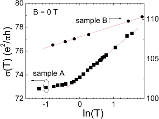
Figure 3. Zero B field conductivity versus ln(T) for sample A (squares) and sample B (dots).
Download figure:
Standard imageTo fit this logarithmic T-dependent data, we again use the formula developed in [37] for non-interacting electrons in graphene. This formula can be simplified for our samples, considering τφ ≫ τ, τi,* and τ, τi,* are nearly temperature independent. The final equation we use for fitting is given by σ(T) = p × e2/πh × ln(T) + constant, where p is the scaling parameter in τφ∝T−p. We shall note that the phonon contribution to the conductivity is not corrected in our fitting. This is justified since the phonon contribution is very small in the temperature range within which we carried out the measurements. The straight line in figure 3 is a linear fit. From the slope of the line, p ≈ 2.3 is obtained.
p ≈ 2.3 is much larger than the value of p = 1 we obtained from the temperature dependence of lφ. This discrepancy strongly indicates the existence of another mechanism that can also produce a logarithmic temperature correction to the electron conductivity. In this regard, we note that it has long been known that e–e interactions contribute a logarithmic T-dependent correction to the electron conductivity at zero B field [23, 38] in ordinary 2DES, with an amplitude of the same order as that due to the quantum interference effect. In a recent study, this e–e interaction effect on the conductivity of graphene was studied [14]. Following the method used in [14], we now include in our conductivity data fitting the e–e interaction correction term δσ = [1 + 3(1 − ln(1 + Fσ0)/Fσ0)] × e2/πh × ln(kBTτ/ℏ),5 where Fσ0 is a measure of e–e interaction. With this new interaction correction term and using p = 1 obtained from the T dependence of lφ, Fσ0 ∼ 0.23 is deduced for sample A.
A smaller but again positive Fσ0 value is obtained in sample B with a higher carrier density. Its low T magnetoresistivity ρxx trace taken at 4 K is shown in figure 4, and SdH oscillations are seen up to Landau level filling ν = 34. From the positions of the SdH oscillation minima, an electron density, ∼2.4 × 1012 cm−2, is deduced. This value is consistent with that obtained from the low B field Hall resistance (not shown). The inset of figure 4 shows the WL phenomenon around B = 0, from which τφ, τi and τ* (or lφ, li and l*) can be obtained. The temperature dependence of lφ for sample B (dots) is shown in figure 2. Unlike in sample A, in sample B lφ shows a much weaker temperature dependence, lφ∝T−1/8. Consequently, a weaker T dependence for τφ, τφ∝T−1/4 (or p = 1/4) is obtained. This weak T dependence for τφ (or lφ) has also been observed in graphene films with high 2DES density [30, 31], and it suggests that decoherence mechanisms other than e–e scattering may be important. The zero field temperature dependence for sample B (dots) is shown in figure 3. Again, a logarithmic temperature dependence is observed for this sample. Similar to sample A, a larger p (p ∼ 1.3 ≫ 1/4) would have been obtained from the linear fit if the e–e interaction term is not included in data fitting. With the interaction correction term, a value of Fσ0 ∼ 0.08 is deduced.
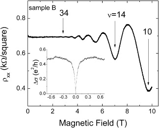
Figure 4. ρxx versus B for sample B. The inset shows Δσ(B) around B = 0.
Download figure:
Standard imageOur data demonstrate that the e–e interaction plays an important role in the zero B field conductivity in our epitaxially grown graphene films. However, a positive value in Fσ0, different from that obtained in exfoliated graphene films [14], was obtained from our transport data. We do not know exactly what is responsible for this discrepancy. On the other hand, different techniques, i.e. exfoliation versus epitaxial growth, were used in obtaining the graphene films in these two experiments. As a result, the disorder configuration and the interplay between the e–e interaction and disorder can be different. Perhaps this difference gives rise to the observed discrepancy in Fσ0.
To summarize, the weak localization phenomenon was studied in two epitaxial graphene films grown on the silicon-faced 6H-SiC substrates at zero and low magnetic fields. Our results show that the e–e interaction plays an important role in carrier conductivity in our epitaxial graphene films.
Acknowledgments
This work was supported by Laboratory Directed Research & Development (LDRD) at Sandia National Laboratories. Sandia National Laboratories is a multi-program laboratory managed and operated by Sandia Corporation, a wholly owned subsidiary of Lockheed Martin Corporation, for the US Department of Energy's National Nuclear Security Administration under contract no. DE-AC04-94AL85000.
Footnotes
- 4
For a recent review on e–e interactions in graphene, see, for example, [7].
- 5
Considering relatively fast intra- and inter-valley scattering rates, we use a coefficient c = 3 in our fitting.